PHYSICAL REVIEW
B
VOLUME 45, NUMBER 20Quantum
size
effects
in
CdS
thin films
15MAY 1992-II
Der-San Chuu
Department
of
Electrophysics, National Chiao Tung University, Hsinchu, Taiwan 30050, Republic ofChinaChang-Ming Dai
Electronics Research & Service Organization, Industrial Technology Research Institute, Chutung, Hsinchu, Taiwan 31015,Republic ofChina
(Received 2October 1991;revised manuscript received 17 December 1991)
Resonant Raman spectroscopy is used to study quantum size effects in CdSfilms. The lattice
soften-ing ofthe CdS LO-phonon mode in a CdS film with a thickness less than 800 A is observed. As the
0 ~ 0
thickness is less than 410A, the TO-phonon mode isobserved at 4880A excitation wavelength, which is
above the band gap ofbulk CdS (2.42 eV)at room temperature. These phenomena are attributed to the size quantization effects ofthe grain size and the low-dimensional thin-film structure. The quantum size
effects cause a blueshift ofthe band gap in the as-deposited CdS thin film. The peak ofthe TO-phonon-mode Raman line ofthe CdSfilm is observed around 220 cm ',which has ashift of8cm 'from the
Ra-man line ofthe most active TO-phonon mode ofbulk CdS. The magnitude ofsoftening energy ofthe TO-phonon mode isobserved tobeindependent ofthe film thickness.
I.
INTRODUCTIONQuantum size effects in semiconductors have attracted
much attention in recent years. ' ' In these investiga-tions, vibrational spectroscopy has played an important
role. The quantum size effect is usually defined as the dependence
of
certain physical propertiesof
a solid on itscharacteristic geometric dimensions when the latter be-comes comparable to the de Broglie wavelength
of
the charge carriers. As the film thickness (measured along the zdirection) ismuch less than the two in-plane dimen-sions (measured in the x-y plane) and is comparable tothe de Broglie wavelength
of
the carriers, quantizationof
the carrier motion in the perpendicular direction to the film plane occurs, although the carrier motion is particle-like in the other two dimensions. Quantum size effects are usually attributed to the small sizeof
microcrystal-lites in the films, ' ' the lower-dimensional thin-film structure,"
' and the effectof
mechanical stress. 'In the last few years, the studies
of
quantum size effects were mainly focused on the observationof
the shiftof
Raman peaks. This is because Raman spectroscopy can probe the local vibrational environment and thus candetermine the presence
of
semiconductor microcrystal-lites inthe films.To
date, several works have discussed the size effectsof
small CdS crystallites with a diameter ranging from 30to 1000A.
Meanwhile, some authors studied the relation-ship between the Raman shift and the filmthick-ness.
"
' Ekimov, Efros, and Onushchenko developed a growth techniqueof
the semiconductor microcrystals in aglassy dielectric matrix which permitted one to vary the sizeof
the grown microcrystals in a controlled manner from some tens to thousandsof
angstroms and thus tostudy the size dependence
of
absorption spectraof
anum-ber
of
semiconductors. Their results showed a consider-able short-wavelength shiftof
the exciton lines was ob-served as the microcrystal size decreased. Ramsteineret al.
"'
studied the hard hydrogenated amorphouscar-bon films on Si by using Raman spectroscopy. They ob-served that the frequency
of
the main Raman peak de-creased for layers thinner than 100 A and applied the term "mode softening" to describe the result. Tu, Wong and Ketterson' studied the thickness dependenceof
the band gap by measuring the resistivity in the intrinsic re-gion. Briiesch etal.
' studied the vibrational propertiesof
thin A1203 films sputtered onto Au, Al, and Si sub-strates by using infrared reflection and absorptionspec-troscopy. They found a softening
of
thelongitudinal-optical
Al-0
stretching mode for a layer thickness less than-500
A.
In this paper we report that the thickness dependence
of
the LO vibrational mode softeningof
the CdS thin films can be observed asfor film thicknesses less than 800A.
Furthermore, the TO-phonon modeof
CdS film can be observed at 4880 A excitation wavelength, which is above the band gapof
bulk CdS (2.42 eV) at room tem-perature asforfilm thicknesses less than410
A.II.
EXPERIMENTThe pulsed laser evaporation (PLE)technique was used
to
produce the CdS thin film on a p-type (100)silicon wafer. In general, the Raman signal is quite sensitiveto
crystal orientation due to selection rules. As shown in a previous paper, thePLE
technique could easily produce the high-quality thin films that yielded sharp Raman peaks. The CdS thin films were grown by aPLE
system which contains a homemade Xe-ion laser'7 (A,=495
nm) operating at about 1 pulse per second with maximum pulsed energyof
10mJ. The laser beam was focused onto a target at about 20' from the surface normalof
the tar-get. The laser fluence was about 1 J/cm and the targetwas moved slightly after hundreds
of
shotsto
prevent causing a sunken spot. A clean vacuum chamber, which was pumped by a 25 liter/sec ion pump, having a base11806 DER-SAN CHUU AND CHANG-MING DAI
pressure
of
3X10
Torr was used. CdS thin films were deposited on the p-type (100)silicon wafers at150'C
sub-strate temperature. The temperature was controlled to fix at
150'C
with the aidof
a temperature controller. The deposition rate was about0.
07A/pulse. CdS powderof
99.
999%
purity was pressed into a pellet which was deliberately left rough so that the couplingof
the laser beam into the target was quite efficient.The crystallinity and surface morphology were identified by x-ray diffraction
(XRD)
and scanning elec-tron microscopy (SEM). These high-orientation films were prepared with a thickness ranging from-80
to-800
A.
The thicknessof
film was measured by using an ellipsometer which has a resolutionof
+10
A.
TheRa-man spectra were recorded by using the unpolarized line
of
4880 Aof
anAr+
laser. Spectra were recorded atroom temperature in 45' reflection geometry with sam-ples being placed under the micrometer stage
of
a triple-grating spectrograph (Spex 1877C) equipped with a liquid-nitrogen-cooled charge coupled devices detectorarray (Photometrics CC200). The incident power on the sample was about 100 mW. The emission spectra
of
Ne andXe
lamps were used for frequency calibration. Theslit width (100pm) used in the experiment led toan
accu-racy
of
3-cm ' resolution.film has wurtzite structure and high orientation in (002) direction even when the substrate isat room temperature.
This result manifests itself in that the clusters in the films have acolumnar structure in the normal direction to the film surface. Figure 2 shows the SEMphotographs
of
the films at substrate temperatures30'C
and150'C.
The re-sults reveal that the surfacesof
the as-deposited CdS films are smooth and uniform. The crystallite sizesof
the CdS films can be either estimated from the SEM photographor calculated by the Scherrer equation:
d=kk, lD
cos8,
where kistaken to be 1forhexagonal CdS, A, isthe x-raywavelength,
D
isthe angular linewidth forhalf-maximum intensity (in radians), and8
is the Bragg angle. These re-sults obtained are-290
A for30'C
and-380
A for150'C.
These are very close tothe results estimated fromthe transmission electron microscopy photographs.
Figure 3 shows the Raman spectra
of
the as-depositedCdS thin films with film thicknesses ranging from 85 to 800A. These Raman spectra were excited by the 4880-A line
of
an Ar+ laser. The spectra show a main CdSRa-man peak (1LO)around 300cm ' as well as the intrinsic Raman scattering (Or)
of
p-type (100)silicon substrate around 520 cm'.
The 1LOphonon frequency for a sin-gle crystalof
CdS was given' as 305 cm',
while the values measured by us were around 300cm'.
This low-frequency shiftof
the 1LORaman peak in CdS thin filmIII.
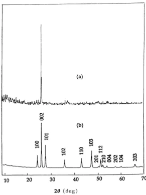
RESULTSAND DISCUSSIONSThe structure and crystallinity were analyzed by
XRD
with a CuEa
source (A,=1.
54 A). Figure 1 shows theXRD
spectrumof
as-deposited CdS film on ap-type (100)silicon wafer at room temperature. One can see that the
(a)
(b)
cV C) CO CD cu0+
hl l 10 I 20 I 30 40 I 50 I 60 70 2&9 (deg)FIG.
1. (a) The XRDspectrum ofthe as-deposited CdSfilmson silicon substrate at room temperature. (b) The pattern of CdS powders.
FIG.
2. The SEMphotographs for the films grown on silicon substrates at temperature (a)30 Cand (b) 100 C.45 QUANTUM SIZE EFFECTSIN CdSTHIN FILMS I I I I 1000
6000-
Si OI 800— C &4000-CO ~~ M CI
c
2000 CdS 1LO 800A 500A 600 g 400-8 200-12 15 i'I I ~ ~ 300 150I g5A 400 500 Raman shift (cm )FIG.
3. Thickness dependence ofthe 1LO phonon energies. These RRS spectra ofCdS films deposited on a p-type silicon0
wafer were excited at 4880A and were detected at room tem-perature. CdS film thickness is indicated in the figure. The dashed line marks the frequency ofthe main Raman peak (300 cm ') for a thick (800 A)film.
has been studied before and is mainly ascribed to the grain-size effect. In
Fig.
3 the spectra reveal as decreas-ing the thicknessof
the CdS films, the silicon Raman peak shifts to the low-frequency region although the amountof
shift is not very evident (around 6 cin ' for 85-A-thick film). The low-frequency shiftof
the silicon Raman peak as the film thickness is less than 800 Amight be ascribed to the stress effect caused by the cou-pling
of
the CdS film and the silicon substrate at thein-terface. As the film thickness
of
CdS increases, the cou-pling effect between the CdS film and the silicon substrateat the interface becomes less prominent. Hence, for CdS films thicker than 800 A, the optical zone center
of
the Raman lineof
silicon resumes eventually to the valueof
520cm '
of
a p-type (100)silicon substrate.From
Fig.
3 it is also found that the main CdS 1LORaman peak shows an increasing shift to the lower-frequency region with decreasing layer thickness. The
shifts
of
the Raman peakof
the 1LOphonon mode as a functionof
the film thicknesses at three excitation ener-gies, 4579, 4880, and 5145 A, are shown inFig. 4.
Onecan note that these shifts are independent
of
the photonexcitation energies and are consistent with the previous works.
"'
FromFig.
4 it can be seen that the Raman shiftsof
the 1LOphonon peakof
CdS films are saturatedto the value
of
5 cm ' when the films are thicker than800 A and the 1LORaman peak has a shift
—
15 cmfor a thin film with 85 A thickness. The saturation
of
1LORarnan shift as film thickness exceeds 800 A is dueto the grain-size effect, as mentioned above. The low-frequency shift
of
the 1LORaman peakof
CdS films as the film isthinner than 800 A might be attributed tothe combinationof
(1) the size effect,'
i.
e., the effectof
size on the vibrational properties in small crystallites and the low-dimensional thin-film structure, and (2)the stress effect induced by the film-substrate interface on thevibra-Shift ofPeak Position (cm')
FIG.
4. Frequency downshifts ofthe 1LO Raman peaks rela-tive toits position forbulk CdS as a function offilm thicknesses. The full curve is drawn to guide the eye. The Raman spectrawere excited at4579,4880,and 5145A.
tional spectrum.
It
is also known that the vibrational mode frequencies vary with increasing temperature. Thus, the Raman shift might be caused by the higher temperature due tothe higher absorptionof
the probe en-ergy in the thicker films. However, this possibility can be ruled out because as we will show later (seeFig.
6) asignificant difference in the absorption cannot happen for
the films having a thickness difference within only an
or-der
of
several hundred angstroms. Thus, the thickness variationsof
the films cannot make a meaningful difference in temperature.The vibrational properties
of
the A1203 thin films on Si and Au have been studied by Briiesch etal.
' They founda softening
of
the longitudinal-opticalAl-0
stretching mode for a layer thickness less than—
100A. For
a 10-A-thick A1203 film a relative mode softeningof
-3%
with respect to the modeof
the bulk crystal was reported.Ramsteiner et
al.
"'
studieda-C:H
on Si using Ramanspectroscopy. They reported that the relative softening
of
a 10-Aa-C:H
film on Siis-4.
5%.
They also found aclear substrate dependence
of
the softening. Our present results yield a relative softeningof
-4.
4%
(with respectto the mode
of
bulk CdS) for a 100-A CdS film on Si wafer. The discrepancy between our results and previous work might be caused by the following. (1) The latticemismatch in CdS/Si system (23.
8%,
lattice constantof
CdS, a axis
=4.
136 A; for Si, 5.43A) islarger than those in a-C:H/Si or A1203/Si systems. The energyof
theLO-phonon mode contains a higher contribution from the
lattice mismatch. (2) The grain-size effect was combined with the thickness effect in our work which was not
con-sidered by the previous works.
"
Figure 5shows the Raman spectra
of
as-deposited CdSthin films with film thicknesses ranging from 700 to 100
A.
These Raman spectra were also excited by the 4880-Aline
of
anAr+
laser. The spectra reveal that there is aTO
mode accompanying the main CdS Raman peak(1LO) around 300 cm ' when the film thickness is less than
410 A.
This TO Raman lineof
the CdS thin film shifts from 228 cm',
the most activeTO
modeof
bulkthick-ll
808 DER-SAN CHUU AND CHANG-MING DAI 45ness. Since the deformation potential is the main mecha-nism
of
the TO Raman scattering, the TO phonon line can be degraded only by the grain-size and stress effects. Therefore, the softeningof
the TO mode (shift from 228 cm 'of
the most active TO modeof
bulk CdS to 220cm ' for a film thinner than 800 A) shown in
Fig.
5 might be ascribed to the combined effectof
the stress and the grain size.It
is well known that the resonant Raman scattering (RRS) cross sectionof
the TO mode has the highest efficiency when the resonant condition is satisfied. ' ' As the photon energy approaches the band gapof
cadmium sulfide, the pronounced decrease in the Raman scattering efficiencyof
the TO mode will be ob-served prior to the onsetof
resonant enhancement. 'The observed decrease in the TOmode as the photon en-ergy approaches the band gap
of
CdS can be interpreted by extending the Loudon theory to include in the Raman-scattering amplitude the destructive interference term between resonant and nonresonant contributions.To
date, TO mode scattering was observed' for pho-ton energyof
a laser beam larger than the band-gap ener-gy. Although the phenomenonof
the disappearanceof
the scattering intensityof
the TO mode for photon ener-gy larger than the band-gap energy is well known,howev-er, the real mechanism still remains unknown. Since the band-gap energy
of
bulk CdS at room temperature (i.e.,25'C)
is 2.42 eV, the TO modeof
the bulk CdS single crystal cannot be observed by using 4880-A (2.54-eV)ex-citation.0 The abnormal occurrence
of
the TO mode at 4880-A excitation in this work might be ascribed to the blueshiftof
the band gapof
a CdS film when the film thickness is less than 700A.
The effectof
reducing film thickness will normally result in the observable high-energy shiftsof
the absorption and transmittance. As shown in Fig. 6,the transmittance propertiesof
CdS thin films deposited on the glasses with various thicknesses100 60
g
40 8 cg 20 C p&p' ~ T . g 400 t 500 1 600 700 800 900 0ranging from 1000 to 4000 A were investigated. We can note from the figure that the absorption edge
of
thinner film is shifted to the smaller-wavelength region (blue-shift). One can also note that the transmittance curves below absorption edges are highly thickness dependent, and the featuresof
these curves agree with the workof
El-Nahass et al.Figure 7 shows the curves
of
the squareof
the absorp-tion coefficienta
versus the photon energy hv by using the results in Fig.6.
As shown in Fig. 7,a
varies linear-ly with hv,and thus the interband transition can be inter-preted by the relationa
=
A(hv
—
E
).To
obtain the valueof
the optical band gap we extrapolated the straight lines inFig.
7 to zero absorption. Results showed that the band-gap energyE
decreases as the thicknessof
theCdS film increases. The blueshifts
of
E
of
CdS films were estimated at about0.
06and0.
16 eVfor thicknessesof
3700and—
1000 A, respectively (comparing with the band gapof
2.42eVof
bulk CdS). Recently, the blueshiftAE caused by the quantum size efFects
of
CdS crystal-lites was measured by Tanahashi etal.
They reportedthat the blueshifts AE are
0.
13 eV for 76-A and-0.
050
eV for 313-Amicrocrystallites embedded in the Si02
ma-trix. Since the grain size
of
our CdS films for differentWavelength (nm)
FIG.
6. Spectral dependence ofthe transmittance for the as-deposited films deposited on glass substrate at different thick-ness. CU ~~ V) CD 50 230A 100A O ~& CL O tA 30-20 10-200300
400500
Raman shift (cm )FIG.
5. Thickness dependence ofthe 1TO phonon intensitiesand energies. The RRS spectra ofCdS films deposited on the p-type (100) silicon wafer were detected at room temperature.
0
The spectra were excited at4880 A.
Q
2.46 2.5P 2.58
Photon Energy (ev)
P..64 P..70
FIG.7. Square ofthe absorption coefficient ofCdSthin films
45 QUANTUM SIZEEFFECTSIN CdSTHIN FILMS 11809 2.0 0 I 1.5 0.5 1.0 8 4P
masked by the envelope
of
the LO signal; and (3) the scattering efficiencyof
the LOmode is larger than the TOmode in the resonant Raman-scattering condition.
It
is worth noting that the scattering efficiencyof
the TOmode overshadows that
of
the LO mode when thickness is less than 150A.
It
is evidence that the Frohlichin-teraction is weak for very thin films, so that LO-mode scattering is mainly caused by the deformation potential.
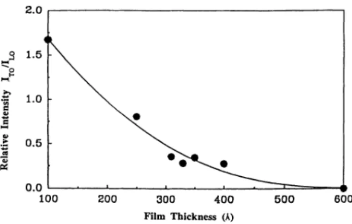
IV. CONCLUSION 0.0 100 200 300 400 Film Thickness (g) 500 4E WF 600
FIG.
8. Thickness dependence ofthe ratio ofthe 1TO inten-sity to the 1LO intensity. The solid line is only a guide to the eyes.0
thicknesses are in the range
of
-300
A, therefore, we conclude that the blueshiftof
0.
06eV for film thickness3700 A might be caused by the grain-size effect
of
the polycrystalline CdS film. Another blueshiftof
-0.
1 eV between the band gapsof
films with thicknesses 3700and—
1000 A can be attributed to the thickness effectof
theCdS films. Therefore, as the thickness is less than 700 A,
the quantum size effect due to the low-dimensional thin-film structure becomes dominant and the band gap
of
the film will blueshiftto
the rangeof
~2.
58eV. Under thiscircumstance, the photon energy
of
2.
54eV (4880A) ly-ing below the band edgeof
the film becomes sufficient forsatisfying the necessary resonance condition
of
the TOmode
of
CdS films.In order to see the thickness effect more clearly, the relative intensity ratio
ITO/I,
„o
as a functionof
film thickness is plotted inFig.
8. We can see that the ratiodecreases when the film thickness increases. One can also note that the Raman signal
of
theTO
mode is insufficientfor observing asfilm thickness is larger than
410 A.
This might be due to (1) the intrinsic thermal broadeningof
the LO Raman peak at room temperature; (2)the intensi-tyof
the LO peak becomes stronger as the film thickness increases and finally the Raman signalof
the TOmode isIn conclusion, the shift
of
the 1LOmode Raman peakto the lower-frequency region as the thicknesses
of
as-deposited CdS films vary from 800 to 85A isascribed tothe size effect (including the lower-dimensional thin-film structure and the grain-size effect
of
the thin films) and the stress effect.For
films thicker than 800 A, the peakof
the 1LO phonon line is at 300 cm ' insteadof
305cm ' for the bulk CdS. This saturation
of
the shiftof
1LORaman peak for films thicker than 800 A is attribut-ed to the effect
of
the grain size.For
thicknesses less than410
A, the TO-phonon mode around 220 cm ' in the CdS thin film can be observed by using 4880-A pho-ton excitation energy which is above the band-gap energyof
bulk CdS. The occurrenceof
the TO-phonon mode is attributed to the quantum size effect because the size quantizationof
free carriers in the lower-dimensional thin-film structure will cause the blueshiftof
the band gap in thin films. The size quantizationof
free carriers is caused by either small-volume microcrystallities or low-dimensional thin-film structure as the film thicknessde-creases. The Raman shift
of
the TOmodeof
CdS films is about 8 cm ' from the Raman peakof
the most activeTO mode
of
bulk CdS. The magnitudeof
this softened energy isfound tobe independentof
the film thickness.ACKNOWLEDGMENTS
One
of
the authors(D.S.C.
) is grateful to ProfessorY.
C.
Leeat SUNY at Buffalo forhis helpful comments. We also thank ProfessorM.
C.
Lee and Professor W.F.
Hsieh for their helpful discussions. This work has been partially supported by the National Councilof
Science, ROCunder Grant No. NSC 80-0208-M-009-25.J. F.
ScottandT.
C.Damem, Opt.Commun. 5, 410 (1972).D. S.Chuu, C. M. Dai, W.
F.
Hsieh, and C.T.
Tsai,J.
Appl. Phys. 69,8402(1991).R.
Rossetti, S.Nakahara, and L.E.
Brus,J.
Chem. Phys. 79, 1086 (1983)~4B.
F.
Variano, N.E.
Schlotter, D.M. Hwang, and C.J.
San-droff,J.
Chem. Phys. 88,2848 (1988).5A. V.Baranov, Ya.S.Bobovich, N.
I.
Grebenshchikova, V.I.
Petrov, and M. Ya.Tsenter, Opt. Spektrosk. 60, 1108 (1986) [Opt. Spectrosc. (USSR)60,685(1986)].H. Jerominek, M. Pigeon, S.Patela, Z.Jakubczk, C. Delisle, and
R.
Tremblay,J.
Appl. Phys. 63, 957(1988).7E.
F.
Hilinski and P.A.Lucas,J.
Chem. Phys. 89,3435(1988). 8A.I.
Ekimov, Al. L.Efros, and A. A. Onushchenko, SolidState Commun. 56,921(1985).
D.V.Murphy and S.
R.
J.
Brueck, Opt. Lett. 8, 494 (1983).G.Kanellis,
J. F.
Morhange, and M.Balkanski, Phys. Rev. B21,1543(1980).
M. Ramsteiner,
J.
Wagner, Ch. Wild, and P.Koidl,J.
Appl. Phys. 62, 729(1987).M. Ramsteiner,
J.
Wagner, Ch. Wild, and P. Koidl, Solid State Commun. 67, 15(1988).Y.
H. Lee,K.
J.
Bachmann,J.
T.
Glass,Y.
M. LeGrice, andR.
J.
Nemanich, Appl. Phys. Lett. 57, 1916 (1990).P.Bruesch,
R.
Kotz,H.Neff,and L.Pietronero, Phys. Rev. B29, 4691(1984).
t5V.B.Sandormirskii, Zh. Eksp. Teor. Fiz.52, 158 (1967) [Sov. Phys. JETP25, 101(1967)].
ll
810 DER-SAN CHUU AND CHANG-MING DAI 45L.W. Tu, G.
K.
Wong, andJ.
B.
Ketterson, Appl. Phys. Lett. 55,1327(1989)~C. M. Qai,
K.
S.Wu, W.F.
Hsieh, and D. S.Chuu, Rev. Sci. Instrum. 61, 3713 (1990).R.
J.
Briggs and A.K.
Ramdas, Phys. Rev.B13, 5518 (1976).R.
C. C. Leite and S.P. S. Porto, Phys. Rev. Lett. 17, 10(1966).
-"R:
H. Cailehaer', S.S.&ussma, ivi. SeitIer's, anti P.K..ChdIlg;— Phys. Rev.B 7,3788(1973).'J.
M. Ralston,R.
L.Wadsack, andR. K.
Chang, Phys. Rev. Lett. 25,814 (1970).R.
Loudon, Proc.R.
Soc.London Ser.A 275,218(1963).J.
F.
Scott,R.
C.C.Leite, andT.
C.Damen, Phys. Rev. 188,1285(1969).
T. C. Damen and
J.
F.
Scott, Solid State Commun. 9,383 (1971).T. C.Damen and
J.
Shah, Phys. Rev.Lett.27, 1506(1971).R.
M.Martin, Phys. Rev. B10,2620(1974).M. M. El-Nahass, O. Jamjoum, S. M. Al-Howaity, and
K.
Abdel-Hady,
J.
Mater. Sci. Lett. 9,79(1990).--r".SaÃMni
mcus.
I .Fdngvicimimi ms6't.'i7vfllcSQQi eh phdBpil=calTransitions in Solids, edited by