Memory effect of RF sputtered ZrO
2
thin films
Chih-Yang Lin, Chung-Yi Wu, Chen-Yu Wu, Chun-Chieh Lin, Tseung-Yuen Tseng
⁎
Department of Electronics Engineering and Institute of Electronics, National Chiao Tung University, Hsinchu 300, Taiwan Available online 17 July 2007
Abstract
Electrical properties of RF sputtered ZrO2memory thin films were investigated in this study. The device with structure Al/ZrO2/Pt shows a
reproducible resistive switching behavior traced over 100 times at room temperature. Moreover, by using various top electrodes, such as Pt, Cu, Ni, Ag, Ti, and even W-probe, the resistive switching phenomenon can be observed in ZrO2-based memory with Pt bottom electrode, indicating
that the ZrO2bulk dominates the resistive switching. The bias polarity dependent resistive switching behavior is demonstrated in the Ti/ZrO2/Pt
device, which might be due to interface reaction between Ti and ZrO2film. The resistance value of high conductive state in the Ti/ZrO2/Pt device
decreases with increasing current compliance implying the possibility for multi-bit storage. Besides, the Ti/ZrO2/Pt device can be operated over
2000 resistive switching cycles at 85 °C by sweeping DC voltage, and the two memory states demonstrate good stability under read voltage stress at room temperature and 85 °C. The write-read-erase-read operations can be over 103cycles at 85 °C. No data loss is found upon successive readout before and after performing 103endurance cycles at 85 °C. According to above experimental results, the ZrO
2thin film has high potential
for nonvolatile memory application. © 2007 Elsevier B.V. All rights reserved.
Keywords: ZrO2; Memory effect; Nonvolatile memory; Resistive switching
1. Introduction
The next-generation nonvolatile memory (NVM) has attracted extensive attention due to the conventional memories approach-ing their scalapproach-ing limits. Several types of NVMs such as ferroelectric random access memory, magnetic random access memory, and resistive random access memory (RRAM) are being investigated. Among various NVMs, the RRAM composed of a simple metal-insulator-metal (M-I-M) structure has the merits of low power consumption, high speed operation and high density integration. Due to these excellent characteristics, a number of metal oxides such as SrZrO3[1,2], Pr1-xCaxMnO3[3], ZrO2[4], TiO2[5,6], CuxO[7,8], and NiO[9–14], have been extensively studied for possible NVM applications.
In this study, we report the effect of top electrode materials on the resistive switching behaviors of the ZrO2thin films. The Ti/ZrO2/Pt device exhibits bias polarity dependent resistive switching. The reliability characteristics of the Ti/ZrO2/Pt device show promising potential for memory application.
2. Experimental procedures
The boron-doped p-type (100) silicon wafer was used to fabricate the memory devices. After the standard Radio Company of America (RCA) cleaning, the 200-nm-thick SiO2 film was thermally grown by a furnace, which was followed by a 20-nm-thick Ti layer and then an 80-nm-20-nm-thick Pt layer deposited by electron beam evaporation at room temperature. Subsequently, about 70-nm-thick ZrO2films were deposited on Pt/Ti/SiO2/Si substrates by an RF magnetron sputter. During deposition process, the substrate temperature was kept at 250 °C and the working pressure was maintained at 10 mTorr by a mixture of Ar and O2at a mixing ratio of 12:6 with a total flow rate of 18 sccm. From the cross-sectional scanning electron microscope (SEM) images as shown inFig. 1, the ZrO2film is observed to possess a columnar structure along the film thickness. Then, various top electrodes, Al, Pt, Cu, Ni, Ag, and Ti with 250μm diameter, were deposited at room temperature by using electron beam evapora-tion or DC magnetron sputtering method through a shadow mask. Electrical properties were measured using an Agilent 4155C and 81110A at room temperature or 85 °C. Current–voltage (I–V) characteristics were measured by the Agilent 4155C. While performing the write-read-erase-read endurance test, the Agilent Thin Solid Films 516 (2007) 444–448
www.elsevier.com/locate/tsf
⁎ Corresponding author.
E-mail address:[email protected](T.-Y. Tseng).
0040-6090/$ - see front matter © 2007 Elsevier B.V. All rights reserved. doi:10.1016/j.tsf.2007.07.140
81110A was adopted to generate voltage pulses to switching the resistance of the device and then the resistance states were checked by the Agilent 4155C. The bias voltage is applied on the top electrode with the Pt bottom electrode grounded. All the measurements were performed under atmosphere condition. 3. Results and discussion
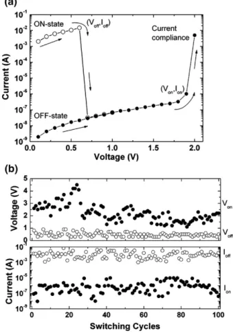
Fig. 2(a) shows the typical I–V curve of Al/ZrO2/Pt device. First, using the DC voltage sweep method with a current compliance of 5 mA, there is a sudden increase of current that occurs near 8.8 V and then limited at 5 mA, which is called forming process (not shown here). Imposing a current compliance is needed to avoid hard breakdown of the resistive switching device. After the forming process, the high conductive state (ON-state) is achieved in Al/ZrO2/Pt device. Further applying a positive voltage to switch the device into low conductive state (OFF-state), an abrupt decrease of current is observed at Voff. Sequentially, applying a positive voltage to translate from OFF-state to ON-state, a sudden increase of current occurs at Vonand then limited at 5 mA. Here, Von, Ion, Voff, and Ioffare defined to trace the resistive switching behavior up to 100 cycles as shown inFig. 2(b), in which the Von has larger variation than Voff. It was previously reported that once the device switched to ON-state, switching back to OFF-state by applying a certain voltage does not guarantee the identical OFF-state due to the stochastic nature of the filament formation and rupture[5]. During ON process(Fig. 2(a)), there is a constant current compliance of 5 mA imposed, which limits the variation of the ON-state resistance and further leads to small variation of the Voff as switching back to OFF-state. While during OFF process, a more random rupture of conducting paths occurred causing the variation of the OFF-state resistance and further leading to larger variation of the Von(Fig. 2(b)) than Voff.
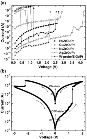
In addition to Al, various metals such as Pt, Ni, Ag, Cu, and Ti are also used for top electrodes to study the properties of ZrO2-based thin film memory devices. According to text-books, the values of work functionψ of these six metals are as follows;ψPt= 5.65 eV,ψNi= 5.15 eV,ψAg= 4.73 eV,ψCu= 4.7 eV, ψAl= 4.3 eV,ψTi= 4.17–4.3 eV. It was reported that if a Schottky
contact was formed between top electrode and NiO film, the effective electric field inside the film was not high enough to induce trapping and detrapping at defect states thus to cause resistive switching [11]. However, after the forming process, which is necessary to activate the resistive switching device, the resistive switching phenomenon can be observed for all the devices using different metals as top electrode in this study, even if the W-probe serves as a top electrode to make a direct contact with ZrO2films as shown inFig. 3(a). Therefore, it assumes that an Ohmic contact is formed between the various metals and ZrO2 film before the forming process or after the forming process, further leading to large enough electric field to induce resistive switching. Kinoshita et al. have proposed that the forming process is equivalent to dielectric breakdown via performing time depen-dent dielectric breakdown test[14]. Hickmott has suggested that an Ohmic contact at both metal/insulator interfaces in the device was formed after breakdown, resulting from the interaction of the metal electrodes with an impurity band in the insulator [15]. Based on above two previous reports, we can conclude that an Ohmic contact is formed between the various metals electrodes and ZrO2before the forming process or after the forming process, and it is the ZrO2film bulk dominating the resistive switching. However, the Ti/ZrO2/Pt device shows bipolar resistive switching behavior inFig. 3(b), which is different from those inFig. 3(a). The physical mechanisms of such resistive switching behaviors still remain open questions. It was reported that the oxygen Fig. 1. The cross-sectional SEM image of the ZrO2/Pt/Ti structure.
Fig. 2. (a) Typical I–V curve of the Al/ZrO2/Pt device. (b) The reproducible
content and the oxygen-related defects had great influences on the resistive switching characteristics [2]. Therefore, the bipolar behavior of the Ti/ZrO2/Pt device might be attributed to that the Ti served as an oxygen gettering material to induce the oxygen vacancies at the Ti/ZrO2 interface, which would modify the oxygen vacancies distribution within ZrO2 memory film bulk further leading to asymmetric trap levels [8]. The detailed mechanism is still under investigation for giving more insight into resistive switching phenomenon.
The successive resistive switching was performed over 2000 times at 85 °C and the result is shown inFig. 4. It indicates that the Ti/ZrO2/Pt device keeps functioning, and gives an indication that the device might be able to be used in COMS circuit.Fig. 5
depicts the electrical properties of the Ti/ZrO2/Pt device under different current compliance conditions. The higher the current compliance imposed on the Ti/ZrO2/Pt device, the higher the current at 0.3 V of ON-state that existed in Ti/ZrO2/Pt, indicating a linear relation between current compliance and current at 0.3 V as shown in the inset ofFig. 5. The linear relation implies the
Fig. 4. The 10th, 100th, and 2000th I–V curves of the Ti/ZrO2/Pt device during successive DC voltage sweeping at 85 °C.
Fig. 5. I–V curves of the Ti/ZrO2/Pt device by imposing various current
compliances, showing the possibility of multi-bit storage application.
Fig. 6. (a) Non-destructive readout test result of both ON- and OFF-states over 104s, and (b) data retention test result of both ON- and OFF-states over 105s at
room temperature and 85 °C under static air. Fig. 3. (a) I–V curves of ZrO2-based memory devices by using Pt, Cu, Ni, Ag,
possibility of the multi-bit application for data storage by an appropriate operation of the Ti/ZrO2/Pt device.
The non-destructive readout test of both ON- and OFF-states for the Ti/ZrO2/Pt device was performed over 104 s at room temperature and 85 °C, indicating that the memory states are stubborn during a-long-time reading and the result is shown in
Fig. 6(a). The retention property, an important characteristic for NVM application, was also measured at room temperature and 85 °C. Both memory states of the Ti/ZrO2/Pt device are stable and maintain their resistance values over 105 s as shown in
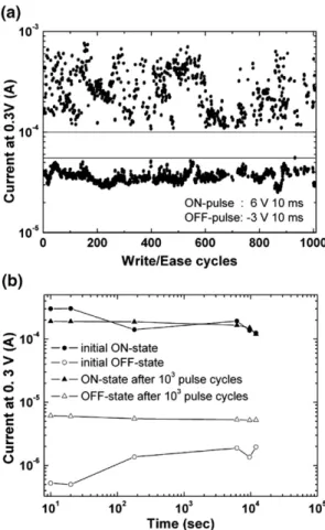
Fig. 6(b). The reliability characteristics of the Ti/ZrO2/Pt device imply promising potential for future memory application. To further investigate the possibility of integrating the Ti/ZrO2/Pt device into CMOS operation; the electrical-pulse-induced resistance change (EPIR) property test was performed at 85 °C. The write-read-erase-read endurance test was achieved by applying a 6 V, 10 ms voltage pulse to switch the Ti/ZrO2/Pt device into ON-state and followed a 0.3 V read step; the other voltage pulse with−3 V, 10 ms was applied to switch back into OFF-state and followed a 0.3 V read step. The write-read-erase-read cycle was performed over 1000 times at 85 °C as shown in
Fig. 7(a). Besides, the non-destructive readout test of both ON-and OFF-states was performed over 104s before and after 103 pulse cycles at 85 °C as shown in Fig. 7(b). The Ti/ZrO2/Pt device shows high possibility to be integrated into CMOS circuit for future NVM application.
In prior work, both ON and OFF processes were in situ monitored during the pulse-switching test, demonstrating the random nature of rupture/formation of conducting filaments in TiO2[6]. Moreover, both memory states are fluctuating during successive pulse cycles, which may be a common phenomenon due to incomplete rupture/formation of filaments [9]. It was reported in Ti/TiN/CuxO/Cu device[7]that OFF-state was more unstable than ON-state, while in our Ti/ZrO2/Pt device, ON-state, however, is more unstable than OFF-state. Therefore, the stability of ON-state and OFF-state would be dependent on the devices themselves (i.e., the resistive switching films and their top/bottom electrode combinations) and the pulse switching conditions (i.e., the pulse width and height used during ON and OFF processes). The effect of the above parameters on the properties of the devices needs further study in order to clarify the stability difference between the two devices mentioned above. 4. Conclusions
In summary, by using various top electrodes such as Pt, Cu, Ni, Ag, Al, Ti, and even W-probe, the resistive switching phenomenon can be observed in ZrO2-based memory with Pt bottom electrode, indicating that the ZrO2bulk film dominates the resistive switching properties. The bias polarity dependent resistive switching behavior was demonstrated in the Ti/ZrO2/Pt device, which might be due to interface reaction. The possibility for multi-bit storage in the device was also discussed. Because the resistance value of high conductive state in the Ti/ZrO2/Pt device decreases with higher current compliance, the multi-bit storage would be implemented by an appropriate operation design. Besides, the Ti/ZrO2/Pt device can be operated over 2000 switching cycles at 85 °C by sweeping DC voltage, and the two memory states demonstrate good stability under read voltage stress at room temperature and 85 °C. The data retention of both high and low conductive states is over 105s at room temperature and 85 °C under static air. Endurance and continuous readout tests are also presented at 85 °C. The write-read-erase-read operations can be over 103cycles and no data loss is found upon successive readout before and after performing 103 pulse cycles. Based on above experimental results, the ZrO2thin film has the high potential for nonvolatile memory application.
Acknowledgement
This work was supported by the Taiwan Semiconductor Manufacturing Company, Ltd., and by the National Science Council, Taiwan, under project NSC 95-2212-E-009-120. References
[1] C.Y. Liu, P.H. Wu, A. Wang, W.Y. Jang, J.C. Young, K.Y. Chiu, T.Y. Tseng, IEEE Electron Device Lett. 26 (2005) 351.
[2] C.C. Lin, B.C. Tu, C.C. Lin, C.H. Lin, T.Y. Tseng, IEEE Electron Device Lett. 27 (2006) 725.
[3] M. Fujimoto, H. Koyama, S. Kobayashi, Y. Tamai, N. Awaya, Y. Nishi, T. Suzuki, Appl. Phys. Lett. 88 (2006) 232106.
Fig. 7. (a) Plots of write-read-erase-read endurance test can be operated over 103 cycles at 85 °C. (b) Plots of non-destructive readout test of both ON- and OFF-states over 104s before and after 103pulse cycles.
[4] C.-Y. Lin, C.-Y. Wu, C.-Y. Wu, T.-C. Lee, F.-L. Yang, C. Hu, T.-Y. Tseng, IEEE Electron Device Lett. 28 (2007) 366.
[5] K.M. Kim, B.J. Choi, D.S. Jeong, C.S. Hwang, S. Han, Appl. Phys. Lett. 89 (2006) 162912.
[6] B.J. Choi, S. Choi, K.M. Kim, Y.C. Shin, C.S. Hwang, S.-Y. Hwang, S.-s. Cho, S. Park, S.-K. Hong, Appl. Phys. Lett. 89 (2006) 012906. [7] A. Chen, S. Haddad, Y.-C. Wu, T.-N. Fang, Z. Lan, S. Avanzino, S.
Pangrle, M. Rathor, W. Cai, N. Tripsas, C. Bill, M. VanBuskirk, M. Taguchi, Int. Electron Devices Meet., Tech. Dig. (2005) 746.
[8] T.-N. Fang, S. Kaza, S. Haddad, A. Chen, Y.-C. Wu, Z. Lan, S. Avanzino, D. Liao, C. Gopalan, S. Choi, S. Mahdavi, M. Buynoski, Y. Lin, C. Marrian, C. Bill, M. VanBuskirk, M. Taguchi, Int. Electron Devices Meet., Tech. Dig. (2006) 789.
[9] I.G. Baek, M.S. Lee, S. Seo, M.J. Lee, D.H. Seo, D.-S. Suh, J.C. Park, S.O. Park, H.S. Kim, I.K. Yoo, U-I. Chung, J.T. Moon, Int. Electron Devices Meet., Tech. Dig. (2004) 587.
[10] S. Seo, M.J. Lee, D.H. Seo, S.K. Choi, D.-S. Suh, Y.S. Joung, I.K. Yoo, I.S. Byun, I.R. Hwang, S.H. Kim, B.H. Park, Appl. Phys. Lett. 86 (2005) 093509.
[11] S. Seo, M.J. Lee, D.C. Kim, S.E. Ahn, B.-H. Park, Y.S. Kim, I.K. Yoo, I.S. Byun, I.R. Hwang, S.H. Kim, J.-S. Kim, J.S. Choi, J.H. Lee, S.H. Jeon, S.H. Hong, B.H. Park, Appl. Phys. Lett. 87 (2005) 263507.
[12] D.C. Kim, S. Seo, S.E. Ahn, D.-S. Suh, M.J. Lee, B.-H. Park, I.K. Yoo, I.G. Baek, H.-J. Kim, E.K. Yim, J.E. Lee, S.O. Park, H.S. Kim, U-In Chung, J.T. Moon, B.I. Ryu, Appl. Phys. Lett. 88 (2006) 202102.
[13] D.C. Kim, M.J. Lee, S.E. Ahn, S. Seo, J.C. Park, I.K. Yoo, I.G. Baek, H.J. Kim, E.K. Yim, J.E. Lee, S.O. Park, H.S. Kim, U-In Chung, J.T. Moon, B.I. Ryu, Appl. Phys. Lett. 88 (2006) 232106.
[14] K. Kinoshita, T. Tamura, M. Aoki, Y. Sugiyama, H. Tanaka, Appl. Phys. Lett. 89 (2006) 103509.