Compensation effect and differential capacitance analysis of electronic energy band
structure in relaxed InAs quantum dots
J. F. Chen, Ross C. C. Chen, C. H. Chiang, M. C. Hsieh, Y. C. Chang, and Y. F. Chen
Citation: Journal of Applied Physics 108, 063705 (2010); doi: 10.1063/1.3467938 View online: http://dx.doi.org/10.1063/1.3467938
View Table of Contents: http://scitation.aip.org/content/aip/journal/jap/108/6?ver=pdfcov Published by the AIP Publishing
Articles you may be interested in
Electronic structure of self-assembled InGaAs/GaAs quantum rings studied by capacitance-voltage spectroscopy Appl. Phys. Lett. 96, 033111 (2010); 10.1063/1.3293445
Electron emission properties of relaxation-induced traps in InAs/GaAs quantum dots and the effect of electronic band structure
J. Appl. Phys. 102, 043705 (2007); 10.1063/1.2770817
Effect of incorporating an InAlAs layer on electron emission in self-assembled InAs quantum dots J. Appl. Phys. 99, 014303 (2006); 10.1063/1.2150258
N incorporation into InGaAs cap layer in InAs self-assembled quantum dots J. Appl. Phys. 98, 113525 (2005); 10.1063/1.2140891
Spin splitting of the electron ground states of InAs quantum dots Appl. Phys. Lett. 80, 4229 (2002); 10.1063/1.1483112
Compensation effect and differential capacitance analysis of electronic
energy band structure in relaxed InAs quantum dots
J. F. Chen,a兲Ross C. C. Chen, C. H. Chiang, M. C. Hsieh, Y. C. Chang, and Y. F. Chen Department of Electrophysics, National Chiao Tung University, Hsinchu, Taiwan 30050,
Republic of China
共Received 25 March 2010; accepted 29 June 2010; published online 17 September 2010兲
The use of a differential capacitance technique for analyzing the effect of strain relaxation on the electronic energy band structure in relaxed InAs self-assembled quantum dots共QDs兲 is presented. Strain relaxation is shown to induce a deep defect state and compensate the ionized impurity in the bottom GaAs layer, leading to a double depletion width and a long emission time. An expression of capacitance at different frequency and voltage is derived for analyzing the experimental data. It has been shown that the relationship between the low-frequency and high-frequency capacitances can be well explained by a Schottky depletion model with a compensated concentration in the bottom GaAs layer. A simple expression is presented to account for the modulation of the free electrons in the top GaAs layer. This capacitance analysis shows a long low-energy tail for the electron ground state, suggesting not very uniform strain relaxation. The results of this study illustrate a carrier compensation effect of the defect state on the electronic energy band structure near the QDs. © 2010 American Institute of Physics.关doi:10.1063/1.3467938兴
I. INTRODUCTION
Understanding the energy band structure in InAs self-assembled quantum dots共QDs兲 共Refs.1–15兲 is important for
designing the QD devices such as photodetectors13,14 or memory devices. In self-assembled InAs QDs, strong strain is built up in the QDs and neighboring GaAs layers. Previous experiments have shown pronounced tunneling emission for the electrons in the QDs escaping to the GaAs.9–11,16,17 The built-up strain is expected to have a strong effect on the energy band structure and emission mechanism of the QDs. Recently, a significantly elongated electron emission time was observed in strain relaxed QDs.18Strain relaxation in the QDs can lead to the generation of threading dislocations in the top GaAs layer and lattice misfits near the QDs.19 Cap-ping the QDs with an InGaAs strain-relieving layer, strain relaxation in the QDs can be accommodated by the lattice misfits near the QDs and the top GaAs layer is dislocation-free.18 Most of the lattice misfits were observed in the bottom GaAs layer under the QDs by transmission electron microscopy,18 suggesting strain relaxation through the bottom GaAs layer. A relaxation-induced defect state at 0.37 eV has been observed in the bottom GaAs layer.19 Un-derstanding the energy band structure in the relaxed QDs is believed to shed light on the strain effect in the coherently strained QDs. Thus, in this paper, we have derived an expres-sion of capacitance at different frequency and voltage to ana-lyze the electronic band structure in the relaxed QDs. We found that the relaxation-induced defect state can compen-sate the background ionized impurity in the bottom GaAs layer, leading to a long emission time. Furthermore, strain relaxation induces a long low-energy tail for the electron ground state共EGS兲 of the QDs, consistent with optical spec-tra. We showed that the energy band structure near the QDs
can be well described by a Schottky depletion mode with a compensated background concentration in the bottom GaAs layer.
II. THEORY
A. Theory of capacitance-voltage„C-V… spectra Based on experimental results, Fig.1shows a simplified electron energy band diagram where Fermi level is intersect-ing with a QD state for a carrier modulation. A relaxation-induced defect state at an energy below the QDs in the GaAs bottom layer is shown. This defect state can trap electrons and compensate the background concentration in the GaAs bottom layer from ionized impurity ND to a compensated background concentration ND
⬘
= ND− Nt, assuming a uniformNtin the bottom GaAs layer for simplicity. This
compensa-a兲Electronic mail: [email protected].
FIG. 1. Simplified electronic energy band diagram for a Schottky diode containing a QD layer for illustrating the modulation of the carriers dQ1at the edge of the depletion region and the carriers dQ2in the QDs at a con-finement energy E. A relaxation-induced defect state Nt is shown in the
GaAs bottom layer.
0021-8979/2010/108共6兲/063705/6/$30.00 108, 063705-1 © 2010 American Institute of Physics
tion can effectively broaden the depletion region in the bot-tom GaAs layer near the QDs and suppress the tunneling emission. Applying a small change in the reverse voltage dV can modulate the carriers共per unit area兲 dQ1 at the edge of the depletion region and the carriers 共per unit area兲 dQ2 in the QDs at a confinement energy E. From Gauss’s law, dV can be expressed by the sum of the voltage changes across the two regions with their respective widths L1 and L2 as follows: dV = dV1+ dV2=
冉
dQ1 冊
L1+冉
dQ1+ dQ2 冊
L2,whereis the permittivity of the semiconductor. In a similar way as derived previously,20 dQ1=dV1/L1 is substituted into the above expression to obtain the ratio of the bias change across L1 to the total bias change as expressed by
dV1 dV = L1 共L1+ L2兲 +dQ2 dV1 L1L2 .
This bias ratio is related to the occupied density of states of the QDs, dQ2/dV1⬅CQ. This density of states is related to capacitance as expressed by CL= dQ1+ dQ2 dV = dQ1 dV + dQ2 dV = dV1 dV L1+ dQ2 dV1 dV1 dV = 共C1+ CQ兲C2 共C1+ CQ兲 + C2 ,
where C1=/L1and C2=/L2are the geometric capacitance per unit area across L1and L2. This equation states that the capacitance is a parallel combination of C1and CQfollowed by a series combination with C2. This shall be the low-frequency capacitance CLif the QD electrons can follow the frequency to be modulated. Under a high frequency where the QD electrons cannot be modulated, CQ= 0 and the ca-pacitance is reduced to CH= C1C2/共C1+ C2兲=/共L1+ L2兲. Thus, the high-frequency capacitance can be used to obtain
L1共L2is the designated spatial position the QDs兲. Substitut-ing L1 into a Schottky depletion model yields the confine-ment energy E of the probed QD electrons as
E = V1+n=共q/2兲ND
⬘
L1 2+共kT/q兲In共NC/ND兲, 共1兲 here ND
⬘
is the compensated concentration in the bottom GaAs layer and Nc is the effective density of states in the GaAs conduction band共CB兲. The applied reverse voltage VR is related to L1 by the voltage drop expression: VR= V1+ V2 − Vbi, where V1=共q/2兲ND⬘
L12 and V2=共q/兲ND⬘
L1L2 +共q/2兲NDL2 2 −共L2/A兲冕
−⬁ E CQdE, 共2兲 here Vbi共=0.8 eV兲 is the Schttoky barrier height of the GaAs and A = 5⫻10−3 cm2 is the area of the diode studied here. The last term in V2 is the voltage drop due to the occupied electrons in the QDs below Fermi level. For simplicity, we have neglected the Fermi–Dirac distribution.Figure 2 shows simulated C-V spectra for a Gaussian carrier distribution CQ共E兲 to represent an electron state in the QD with a peak of 680 pF 共=8.6⫻1011/cm2, eV兲 at E = 0.252 eV with a broadness of 70 meV. This carrier distri-bution CQ共E兲 gives a total carrier density of 7.9 ⫻1010 cm−2, which is close to double the QD density cor-responding to a capture of two electrons for an EGS. The simulation uses ND= 1⫻1017 cm−3 and ND
⬘
= ND− Nt= 2.9 ⫻1016 cm−3 based on the experimental data to be shown. The simulated CLdisplays a protrusion from⫺2 to ⫺3.5 V with a peak at ⫺2.8 V, corresponding to the modulation of the peak of CQ共E兲 at E=0.252 eV.We would like to emphasize that the above derivation works for large amplitude of reverse voltage so that the top GaAs layer is totally depleted of free electrons. For small amplitude of reverse voltage, Fermi level also modulates the free electrons in the top GaAs layer and introduce additional capacitance CGaAs= dQGaAs/dV1, where QGaAs is the modu-lated electron density in the top GaAs layer and shall be approximately proportional to the free carrier concentration at the GaAs CB near the QDs, no= NCexp共−V1/kT兲 here
V1=共q/2兲ND
⬘
L1 2. Decreasing reverse voltage will increase
V1to deplete QGaAsby QGaAs= QGaAs,oexp共−V1/kT兲. Accord-ingly, this additional capacitance rapidly decreases with in-creasing V1 by CGaAs= dQGaAs/dV1=共1/kT兲QGaAs = CGaAs,oexp共−V1/kT兲. This effect is appreciable only when
V1共L1兲 is very small. Under this condition, the modulated
free carriers are nearly at the same spatial location as the QDs, leading to the low-frequency capacitance can be ap-proximately expressed by CL⬵C2+ CQ+ CGaAs while CH ⬵C2. Thus, the effect of the carrier modulating in the top GaAs layer can be simply removed by subtracting CGaAs = CGaAs,oexp共−V1/kT兲 from CL. This effect, if not removed, would lead to an overestimation of the carrier density in the shallow QD electrons. This free carrier modulation effect is significant in the relaxed QDs because of the broad carrier depletion near the QDs.
III. MEASUREMENT AND RESULTS
The InAs QD samples were grown by solid source mo-lecular beam epitaxy in a Riber machine. On top of a n+-GaAs共100兲 substrate, a 0.3 m-thick Si-doped GaAs 共
FIG. 2. Simulated low-frequency and high-frequency C-V spectra for a Gaussian carrier distribution CQ共E兲 at a depth of 0.2 m at E = 0.252 eV
with a broadness of 70 meV. The low-frequency spectra display a C protru-sion peaked at⫺2.8 V.
063705-2 Chen et al. J. Appl. Phys. 108, 063705共2010兲
⬃1⫻1017 cm−3兲 barrier layer, an InAs layer with different deposition thickness from 2 to 3.3 monolayer共ML兲 was de-posited at 490 ° C 共at a rate of 0.26 Å/s兲 to form the QDs. Following the growth of the QDs layer, a 60 Å In0.15Ga0.85As strain-relieving capping layer and a 0.2 m-thick Si-doped GaAs 共⬃1017 cm−3兲 barrier layer were grown to terminate the growth. Relaxation in the QDs was achieved by increas-ing the InAs deposition thickness slightly beyond a critical thickness about 3 ML. A photoluminescence共PL兲 blueshift21 about 80 meV is observed when strain relaxation in the QDs occurs. The QD sheet density is estimated to be ⬃3 ⫻1010 cm−2 from performing atomic force microscopy on sample surface where a layer of similar QDs was purposely grown. For C-V profiling, Schottky diodes were realized by evaporating Al on sample surface with an area 5 ⫻10−3 cm2. A HP 4194A impedance analyzer was used for
C-V measurements with an oscillation level set at 50 mV.
A. C-V-F spectra
1. Coherently strained QDs
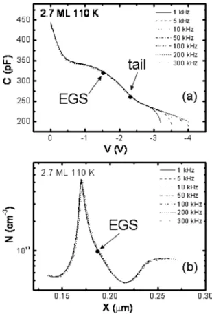
Figures3共a兲and3共b兲shows the 110 K C-V and its con-verted carrier distribution using:N共w兲=共C3/q0共dC/dV兲兲 for a nonrelaxed QD diode with InAs deposition thickness of 2.7 ML. A C plateau from⫺0.5 to ⫺2.5 V, corresponding to the modulation of the QD electrons, is visible. This plateau can be dissolved into a peak and a shoulder in the carrier distribution plot. The peak is attributed to the QD first ex-cited state and the shoulder to the EGS of the QDs. When
temperature is lowered to 90 K, the shoulder displays fre-quency dispersion with an activation energy about 60 meV, suggesting a tunneling emission through the first excited state.18 The emission energy of the first-excited state cannot be obtained from the C-V spectra because no frequency dis-persion is observed共the emission time is very short兲. We can estimate the confinement energy for the tail of the EGS be-cause, at this nearly ending of modulation, the low-frequency capacitance shall approach the high-frequency capacitance. Let us choose C = 245 pF at⫺2.5 V as the tail of the QDs. This C gives L1+ L2= 0.234 m 共L2= 0.16 m is the de-signed QDs position from the surface兲. Substituting L1 = 0.074 m and a ND= 8⫻1016 cm−3for ND
⬘
共seen in the car-rier distribution兲 into Eq.共1兲yields E = 0.320 eV共at 110 K兲. As shown in Fig.4, the 50 K PL spectra of this sample show a ground emission at 1250 nm共0.992 eV兲 with a narrow full width at half maximum of 35 meV. If we take this broadness as the broadness of the EGS, the EGS shall be at 0.303 eV. This gives the confinement energy of the hole ground state 共HGS兲 of 1.50−0.992−0.303=0.205 eV, giving rise to a ra-tio of the confinement energy of EGS to HGS of 0.60 to 0.40, a value close to a previously reported 0.61:0.39.22The confinement energy of the EGS in the relaxed QDs shall be slightly smaller than that 共0.303 eV兲 of the nonrelaxed QDs because the PL spectra show a blueshift of 79 meV when the relaxation occurs.21Figure 4shows the PL ground emission at 1.071 eV for the relaxed QDs. This blueshift could move the EGS to 0.256 eV in the relaxed QDs assuming the above ratio of 0.6:0.4. This rough estimation shows that the EGS of the relaxed QDs shall be around 0.256 eV.2. Relaxed QDs
Figures5共a兲and5共b兲 show the 110 K C-V and the con-verted carrier distribution for a relaxed QD diode with InAs deposition thickness of 3.3 ML. Its 50 K PL spectra are shown in Fig. 4. The C-V spectra display two C plateaus. The plateau from ⫺1.5 to ⫺3.4 V is attributed to the QD electrons since its converted carrier profiling displays a simi-lar feature as observed in the nonrelaxed QDs as follows: a peak at 0.217 m from the first excited state共the QD spatial position is designed at 0.2 m兲, and a shoulder at 0.225 m from the EGS. In contrast to no frequency dispersion ob-served in the nonrelaxed QDs, the C-V spectra of the relaxed
FIG. 3. 共a兲 110 K C-V and 共b兲 the converted carrier distribution for a nonrelaxed QD diode with InAs deposition thickness of 2.7 ML, illustrating a C plateau from⫺0.5 to ⫺2.5 V related to the modulation of the QD electrons.
FIG. 4. 50 K PL spectra for nonrelaxed QDs with InAs deposition thickness of 2.7 ML and relaxed QDs with InAs deposition thickness of 3.3 ML. Strain relaxation causes a blueshift in the ground emission and produces a long low-energy tail.
QDs display frequency dispersion, suggesting a longer emis-sion time. As shown in Fig.5共a兲, the C protrusion diminishes with increasing frequency, reflective of an incapability of carrier modulation. Note that we observed no appreciable change in the C-V spectra when frequency is lower than 1 kHz or higher than 200 kHz, and thus we take C at 1 kHz as
CL and at 200 kHz as CH for the following analysis. The 0.217 m 共at ⫺2.54 V兲 for the first excited state and the 0.225 m共at ⫺2.8 V兲 for the EGS cannot be interpreted as the positions of the edge of the depletion region because the concentration profiling in Fig. 5共b兲 is converted from the low-frequency capacitance which is affected by the modula-tion of the QDs. We should use the high-frequency capaci-tance. Figure5共a兲shows CH= 196 pF at⫺2.54 V 共186 pF at ⫺2.8 V兲, which gives L1+ L2= 0.293 m共0.308 m兲. After substituting from L2= 0.2 m 共the QDs position from the surface兲, we obtain L1= 0.093 m共0.108 m兲. Substituting these L1 and ND
⬘
= 2.9⫻1016 cm−3 共to be determined in a later section兲 into Eq. 共1兲 yield confinement energies of E = 0.189 eV and 0.252 eV for the first-excited state and EGS, respectively. The energy for the EGS is consistent with the one 共0.256 eV兲 estimated from the nonrelaxed QDs. Note that, during the simulation 共in Fig. 2兲, an electron state at0.252 eV would result in a C plateau peaked at⫺2.8 V. As shown in Fig.5共a兲, the QD plateau is immediately followed by another C plateau 共starting at ⫺3.5 V兲 which shows no frequency dispersion, suggesting an emission time
too long to be modulated. This plateau is attributed to the relaxation-induced defect state previously identified at 0.37 eV below the GaAs CB by deep-level transient spectroscopy.19 The nearly voltage-independent capacitance suggests a pinning of Fermi level, implying a density of states being comparable to the background ionized impurity. Figure5共b兲shows drastic carrier depletion after the QD, sug-gesting a lower background concentration due to the carrier compensation of this defect state. Further decreasing reverse voltage will push down Fermi level to intersect with the defect state, giving rise to the second plateau at⫺3.5 V 共and the converted carrier peak兲 until all the trapped electrons are swept out of the defect state. This defect state behaves like a point defect state whose properties were previously studied in details.19 It is similar as the one 共0.395 eV, = 1 ⫻10−16 cm2兲 observed by Uchida et al.23
in strain relaxed InGaAs/GaAs quantum well structures. The fact that the tail of the QD共at ⫺3.4 V兲 is immediately followed by the defect state stipulates that the tail of the EGS shall have a confine-ment energy of⬃0.37 eV.
B. Compensation of background concentration One pronounced feature associated with the defect state is the asymmetric carrier distribution on the sides of the QDs, as shown in Fig.5共b兲. The top GaAs layer displays a normal carrier depletion near the QDs and a designated back-ground concentration of ND= 1⫻1017 cm−3. On the other hand, the bottom GaAs layer displays a lower background concentration with a nearly double depletion width, suggest-ing a compensation of the ionized impurity by the defect state. Based on a simple Schottky depletion model V =共q/2兲NDL2, a double depletion width would require a re-duction in the background concentration from 1⫻1017 to 2.5⫻1016 cm−3, leading to an effective trapped concentra-tion Nt= 7.5⫻1016 cm−3.
We can obtain a more accurate compensated concentra-tion ND
⬘
by using the voltage drop relationship: VR= V1+ V2 − Vbi in Eq. 共2兲. At ⫺3.4 V, the QDs are nearly empty of carriers and thus the term共L2/A兲兰−E⬁CQdE in Eq.共2兲can be neglected. Figure 5共a兲shows CH= 173 pF at⫺3.4 V, corre-sponding to L1= 0.132 m. Substituting the L1, L2 = 0.2 m, VR= 3.4 V and Vbi= 0.8 V into Eq. 共2兲 givesND
⬘
= 2.9⫻1016 cm−3. This is close to the value 共2.5 ⫻1016 cm−3兲 estimated from a double depletion width in the bottom GaAs layer. Substituting this ND⬘
and L1= 0.132 m into Eq. 共1兲 yields E = 0.364 eV 共at 110 K兲. This energy, obtained from nearly the end of the modulation of the QDs, shall correspond to the tail of the EGS. As mentioned above, this energy shall be close to that of the defect state共0.37 eV兲 because Fig. 5共a兲shows that the tail of the QD is immedi-ately followed by the defect state. This consistency supports the validity of using a compensated concentration in a Schottky depletion model to describe the electronic energy band in the bottom GaAs layer near the QDs. Note that we have used this compensated background concentration ND⬘
= 2.9⫻1016 cm−3 to obtain the confinement energy of the EGS which is E = 0.252 eV. This energy and the PL ground emission共1.078 eV at 110 K兲 results in the confinementen-FIG. 5. 共a兲 110 K C-V and 共b兲 the converted electron distribution for a relaxed QD diode with InAs deposition thickness of 3.3 ML. The C plateau from⫺1.5 to ⫺3.4 V is related to the modulation of the QD electrons and the C plateau starting from ⫺3.5 V is related to the relaxation-induced defect state.
063705-4 Chen et al. J. Appl. Phys. 108, 063705共2010兲
ergy of a HGS of 1.50− 1.078− 0.252= 0.170 eV, giving rise to a ratio of the confinement energy of EGS to HGS of 0.60 to 0.40, in agreement with a ratio obtained from the nonre-laxed QDs. Note that this ND
⬘
= 2.9⫻1016 cm−3was also used for the simulation in Fig.2to produce a C plateau peaked at ⫺2.8 V from an electron state at 0.252 eV.The EGS at 0.252 eV with its tail at 0.364 eV suggests a tail as wide as 112 meV. A long low-energy tail is also seen in the PL ground emission of the relaxed QDs in Fig. 4, which display a tail extending to about 1300 nm, about 117 meV from the peak of the ground emission at 1.071 eV. Note that this long low-energy tail is not seen in the nonrelaxed QDs, and thus it is related to strain relaxation. Strain relax-ation can enhance the flucturelax-ation of the QD states and form a long low-energy tail, suggesting the process is not very homogenous.19 Note that the carrier compensation effect caused by the relaxation-induced defect state can increase L1 from 0.074 to 0.132 m at the tail of the EGS. This, along with the reduction in NDfrom 8⫻1016 to 2.9⫻1016 cm−3, would reduce the electric field at the QD from 8.2⫻106 to 5.3⫻106 V/m from the expression E=共q/兲N
D
⬘
L1. As a sult, the tunneling emission is significantly suppressed, re-sulting in a long emission time in the relaxed QDs.C. Effect of the free carrier modulation in the top GaAs layer
Probably due to the large L1, the free electrons in the top GaAs layer when they traverse through the QD region to the bottom GaAs layer will exert an observable time constant. The C-V spectra in Fig. 5共a兲 display frequency dispersion from 0 to ⫺1.5 V 共with a nearly temperature-independent inflexion frequency of about 6⫻105 Hz determined from
C-F spectra兲. As explained in the section of the theory, this is
the modulation of the free electrons in the top GaAs layer with CL= C2+ CGaAs and CH= C2. The CGaAs= CL− CH = 40 pF at the starting modulation of the QDs共at ⫺1.5 V兲 gives QGaAs= 4.8⫻108/cm2 from CGaAs=共1/kT兲QGaAs. This free-carrier modulation effect if not removed would lead to an overestimation of the electron density for the shallow QD electrons. This modulation diminishes rapidly with reverse voltage by CGaAs= CGaAs,oexp共−V1/kT兲. For example, this effect decays to e−1when the applied voltage probes the QD electrons at E = 36 meV 共V1= 9.5 meV at 110 K兲. Thus, it affects only the shallow QD electrons. At around⫺1.5 V, C1 can be considered not exist 共L1→0兲 and CL= C2+ CQ + CGaAsand CH= C2. Thus, we remove this free carrier modu-lation effect by subtracting CL from CGaAsand the result is shown in the dashed curve in Fig.6. In this figure, we have converted the reverse voltage to the confinement energy E of the QD from the high-frequency capacitance as shown in the inset. From the lowest frequency of 1 kHz which allows the modulation of all the QD electrons, the QD electrons are filled from⬃0.38 eV to the GaAs CB edge. In the figure, we have marked the EGS and first excited state of the QDs based on the PL spectra. From CL=共共C1+ CQ兲C2/共C1+ CQ兲 + C2兲 shown in the theory, we obtained CQand estimated the
total electron density about 2⫻1011 cm−2. Thus, each QD contains about eight electrons 共QD density= ⬃3 ⫻1010 cm−2兲.
IV. CONCLUSIONS
We present a differential capacitance analysis to estab-lish the electronic band structure in strain relaxed InAs QDs. Strain relaxation can introduce a deep defect state to com-pensate the ionized impurity in the bottom GaAs layer, re-sulting in a wide depletion width and a long emission time. We show the validity of using a compensated background concentration in a Schottky depletion model to describe the electronic energy band in the GaAs bottom layer. The EGS of the QDs is obtained to be 0.252 eV, giving a ratio of the confinement energies of the electron to HGSs of 0.60 to 0.40. This analysis shows the presence of a long tail for the EGS of the QDs, consistent with the PL spectra.
ACKNOWLEDGMENTS
The authors are grateful to Dr. J. Y. Chi and R. S. Hsiao for sample preparation and would like to thank the National Science Council of the Republic of China, Taiwan for finan-cially supporting this research under Contract No. NSC-97-2112-M-009-014-MY3. This work is partially supported by MOE ATU program.
1F. Heinrichsdorff, M. H. Mao, N. Kirstaedter, A. Krost, and D. Bimberg,
Appl. Phys. Lett.71, 22共1997兲.
2D. J. Eaglesham and M. Cerullo,Phys. Rev. Lett.64, 1943共1990兲. 3D. Leonard, K. Pond, and P. M. Petroff,Phys. Rev. B50, 11687共1994兲. 4J. M. Moison, F. Houzay, F. Barthe, and L. Leprince,Appl. Phys. Lett.64,
196共1994兲.
5C. W. Snyder, J. F. Mansfield, and B. G. Orr, Phys. Rev. B46, 9551 共1992兲.
6H. Shoji, K. Mukai, N. Ohtsuka, M. Sugawara, T. Uchida, and H. Ish-ikawa,IEEE Photon. Technol. Lett.7, 1385共1995兲.
7G. Yusa and H. Sakaki,Electron. Lett.32, 491共1996兲.
8J. C. Campbell, D. L. Huffaker, H. Deng, and D. G. Deppe,Electron. Lett.
33, 1337共1997兲.
9C. M. A. Kapteyn, F. Heinrichsdorff, O. Stier, R. Heitz, M. Grundmann, and P. Werner,Phys. Rev. B60, 14265共1999兲.
10P. N. Brunkov, A. Patane, A. Levin, L. Eaves, P. C. Main, Y. G. Musikhin, B. V. Volovik, A. E. Zhukov, V. M. Ustinov, and S. G. Konnikov,Phys. Rev. B65, 085326共2002兲.
11W. H. Chang, W. Y. Chen, T. M. Hsu, N. T. Yeh, and J. I. Chyi,Phys. Rev.
B66, 195337共2002兲.
FIG. 6. Measured capacitance vs the confinement energy of the QD elec-trons converted from Fig.5共a兲 using the high-frequency capacitance. The inset shows the converted relationship between reverse voltage and the con-finement energy.
12X. Letartre, D. Stievenard, and M. Lanoo,J. Appl. Phys.69, 7336共1991兲. 13H. Drexler, D. Leonard, W. Hansen, J. P. Kotthaus, and P. M. Petroff,
Phys. Rev. Lett.73, 2252共1994兲.
14S. Sauvage, P. Boucaud, F. H. Julien, J.-M. Gerard, and J.-Y. Marzin,J.
Appl. Phys.82, 3396共1997兲.
15H. L. Wang, F. H. Yang, S. L. Feng, H. J. Zhu, D. Ning, H. Wang, and X. D. Wang,Phys. Rev.61, 5530共2000兲.
16J. Ibáñez, R. Leon, D. T. Vu, S. Chaparro, S. R. Johnson, C. Navarro, and Y. H. Zhang,Appl. Phys. Lett.79, 2013共2001兲.
17J. F. Chen, R. S. Hsiao, C. K. Wang, J. S. Wang, and J. Y. Chi,J. Appl.
Phys.98, 013716共2005兲.
18J. F. Chen, Y. Z. Wang, C. H. Chiang, R. S. Hsiao, Y. H. Wu, L. Chang, J. S. Wang, T. W. Chi, and J. Y. Chi,Nanotechnology18, 355401共2007兲.
19J. F. Chen and J. S. Wang,J. Appl. Phys.102, 043705共2007兲.
20J. F. Chen, N. C. Chen, J. S. Wang, and Y. F. Chen,IEEE Trans. Electron
Devices48, 204共2001兲.
21J. F. Chen, R. S. Hsiao, Y. P. Chen, J. S. Wang, and J. Y. Chi,Appl. Phys.
Lett.87, 141911共2005兲.
22S. D. Lin, V. V. IIchenko, V. V. Marin, K. Y. Panarian, A. A. Buyanin, and O. V. Tretyak,Appl. Phys. Lett.93, 103103共2008兲.
23Y. Uchida, H. Kakibayashi, and S. Goto,J. Appl. Phys.74, 6720共1993兲.
063705-6 Chen et al. J. Appl. Phys. 108, 063705共2010兲