Coverage Analysis for the Core/Shell Electrode of Dye-Sensitized Solar Cells
Ta-Chang Tien,*,†Fu-Ming Pan,*,†Lih-Ping Wang,‡Feng-Yu Tsai,§and Ching Lin§ Department of Material Science and Engineering, National Chiao Tung UniVersity, Taiwan, 300, ROC, PhotoVoltaics Technology Center and Nanotechnology Research Center, Industrial Technology Research Institute, Taiwan, 310, ROC, and Department of Materials Science and Engineering,National Taiwan UniVersity, Taiwan, 106, ROC
ReceiVed: March 15, 2010; ReVised Manuscript ReceiVed: April 16, 2010
In this study, we established a core/shell (C/S) model that evaluates the surface coverage of an overlayer deposited on nanoparticles in terms of X-ray photoelectron spectroscopy signals of the nanoparticles. We used the model to estimate the coverage of Al2O3shell layers, which were deposited on the nanoporous TiO2 electrodes of dye-sensitized solar cells (DSSCs) by atomic layer deposition (ALD), as a function of the number of ALD reaction cycles. The surface coverage increased with the average thickness of the Al2O3shell layers, indicating that the ALD Al2O3deposition on the nanoporous electrode was via the island growth mode. The power conversion efficiency of the DSSCs was highest after the first ALD reaction cycle for the Al2O3shell layers, which had a coverage of 0.25, according to the C/S model. The study shows that, to further improve the PCE, optimization of the ALD Al2O3deposition condition is required so that the surface coverage of the shell layer can be increased at the first ALD reaction cycle.
I. Introduction
Nanoporous materials possessing core/shell (C/S) structures are attracting great interest because of their promising applica-tion in catalysis, sensors, batteries, fuel cells, and solar cells.1-5
Among the most popular of these applications, dye-sensitized solar cells (DSSCs) based on nanoporous electrodes comprising interconnected TiO2nanoparticles exhibit an enhancement (by
10-35%) in the power conversion efficiency (PCE) when Al2O3
shell layers cap on TiO2 nanoparticles.6-8 The improved
performance of DSSCs featuring Al2O3shell layers is based on
decreases in the degrees of charge recombination and electron transfer from the dye through the Al2O3 overlayers via a
tunneling effect.9-13The increased PCE of dye-sensitized TiO 2
solar cells featuring Al2O3shell layers with an optimal thickness
is related to their interfacial energy levels, that is, the high recombination energy barrier of the Al2O3-TiO2interface, the
high work function of the Al2O3overlayers, and the low energy
barrier between the dye and Al2O3. Optimization of the
Al2O3-TiO2 interface in DSSCs can be performed using
different coating procedures, which so far have relied on the good coverage of the shell layer of the nanoporous electrode. Atomic layer deposition (ALD) is usually considered an ideal method to deposit ultrathin films of high uniformity and conformity and, therefore, is presumed to be able to achieve an excellent PCE enhancement when it is used to coat the Al2O3
shell layer on nanoporous TiO2 electrodes. However, in a
previous study,14we found that the PCE enhancement for our
DSSCs featuring the ALD Al2O3shell layers is not better than
that for DSSCs with Al2O3 shell layers prepared by other
methods, such as sol-gel coating.3,7-9We ascribed the
unsat-isfactory PEC enhancement to a low coverage of the ALD Al2O3
shell layers on the nanoporous TiO2electrodes as a result of
that the island growth mode prevails during the ALD deposition. To further optimize the PCEs of DSSCs featuring Al2O3/TiO2
electrodes, it will be necessary to know well the dependence of the coverage of the Al2O3overlayers on the number of ALD
deposition cycles. However, to correctly determine the coverage of an ultrathin Al2O3 layer coated on a porous electrode is
difficult because there is presently no reliable analytical tool for the measurement. For instance, information provided by TEM analysis with an atomic scale resolution is limited to a localized area, and sample damage may occur during TEM sample preparations.
X-ray photoelectron spectroscopy (XPS) has a very small probe depth (<10 nm) and is often used to determine the coverage of an ultrathin film on a flat substrate in terms of measuring XPS signals of the substrate as a function of the amount of deposited film materials.15,16However, XPS becomes
less straightforward when the coverage on a curved substrate, such as a particle, is studied. Theoretical models based on XPS to evaluate the coverage of an ultrathin layer on a particle usually requires an elaborate mathematical derivation with complex geometric considerations.17,18This is particularly so for ultrathin
films deposited on porous substrates composed of interconnected nanoparticales. The purpose of this study is to develop a multilayer C/S model, using XPS, to measure the coverage of shell layers on the nanoporous electrodes of DSSCs. The model treats only the zenith angle in the mathematic derivation in terms of spherical symmetry considerations; therefore, the derivation is simpler compared with other models.17-20 This model
resembles more a real C/S material system as in the case of the porous TiO2electrode. Using these characterization techniques,
we studied the influence of the coverage of the Al2O3shell layers
on the PCE of our DSSCs. II. Theoretical Model
Like several previous reported models17-20that relate the
adsorbate coverage on a spherical particle to the XPS signal emitted from the particle, the basic concept of our core/shell
* To whom correspondence should be addressed. E-mail: [email protected] (T.-C.T.), [email protected] (F.-M.P.).
†National Chiao Tung University. ‡Industrial Technology Research Institute. §National Taiwan University.
10.1021/jp1023229 2010 American Chemical Society
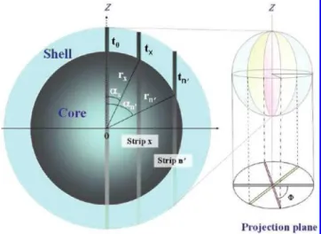
model divides the nanoparticle, which is assumed to be spherical, into many small partitions and considers separately the XPS signal emitted from each partition. In this model, numerous identical circular planes can be constructed from a sphere, as shown in Figure 1, in which the projections of three such circular planes at different azimuth angles (φ) are illustrated. The symmetrical geometry of the spherical particle allows us to exclude the participation of the φ angle in the derivation of the relation of the shell coverage with the XPS signal emitted from the core, thus only a circular plane at a fixed φ angle is taken into account to derive the relation. The circular plane is divided into 1000 strips with the long axis perpendicular to the sample surface. As shown in Figure 1, the thickness of the shell (tx) in a strip, for example, strip
x, depends on the strip angle (Rx) between the strip passing
through the origin of the circle (O) and the line connecting point O with the intersecting point of strip x and the circle. Each strip is so thin that we may consider, within the strip, that the surface of the core particle is flat. Because the hemispherical energy analyzer is located from the sample at a distance much larger than the sample size, we assume that electrons emitted from all the strips have the same emission angle, which is 0° under the present analysis configura-tion.
In a previous study,14we found that ALD Al
2O3deposition
on the porous TiO2 electrode followed the island growth
(Volmer-Weber) mode according to a plot of the growth per cycle versus the number of ALD reaction cycles. On the basis of Sitar’s study,16 the dependence of XPS signals of a flat
substrate on the island coverage (θisland) can be expressed as
the following equation
where Ιsand Ι0are the intensities of photoelectrons emitted from
the substrate with and without the thin film material, respec-tively, n is the number of monolayers in an island, a is the thickness of each monolayer, and λ is the inelastic mean free path (IMFP) of electrons traveling in the overlayer. Assuming a uniform coverage, we replace θislandwith the coverage of the
shell material (fractional coverage, θ) on the two ends of each strip and introduce the strip angle (Rx) for the thickness
calculation, and thus, eq 1 can be converted into the following expression
where ∆Ι and ∆ΙRare the intensities of photoelectrons emitted
from a single strip with and without the shell layer, respectively,
t is the thickness of the shell layer, R is the strip angle (θ values
from 0° to 90°), and λshellis the inelastic mean free path (IMFP)
of electrons traveling in the shell layer. We assume in this model that θ is the same for all the 1000 strips because of the homogeneous deposition nature of ALD. By summing up the values of ∆Ι of all strips in terms of R (from θ ) 0° to θ ) 90°), we obtained an equation representing the total intensity (I) of photoelectrons emitted from the entire half part of the circular plane with the shell layer as follows:
The value of ∆IR can be calculated using the following
equation20
where ∆Ibulkrepresents the intensity of the photoelectrons from
a strip of infinite length (relative to λcore), r is the radius of the
circular plane, and λcoreis the IMFP of electrons traveling in
the core particle. In this study, the radius of the core particle is around 10 nm. Substituting eq 4 into eq 3, we obtain
At the boundary conditions (t ) 0, θ ) 0)
where I0is the intensity of photoelectrons from the circular plane
without the shell layers. Because ∆Ibulkis independent of angle
R, eq 6 can be rewritten and converted into
Substituting eq 7 into eq 5, we obtain
Figure 1. C/S model for calculating the fractional coverage (θ) of
shell layers from an isolated C/S particle. The left circular plane is the cross-sectional plane that produces a projection line at a certain azimuth angle.
Is/I0) (1 - θisland) + θisland× e-na/λ (1)
∆I/∆IR) (1 - θ) + θ × e-t/(λshell×cosR) (2)
I )
∑
R)0° 90° ∆I )∑
R)0° 90°{∆IR× [(1 - θ) + θe-t/(λshell×cosR)]}
(3)
∆IR) ∆Ibulk× [1 - e
(-2rcosR/λcore)] (4) I )
∑
R ) 0° 90° {∆Ibulk× [1 - e (-2rcosR/λcore)]× [(1 - θ) +θe-t/(λshell×cosR)]} (5)
I ) I0)
∑
R ) 0° 90° {∆Ibulk× [1 - e (-2rcosR/λcore)]} (6) ∆Ibulk) I0÷∑
R ) 0° 90° [1 - e(-2rcosR/λcore)] (7) I I0 )∑
R ) 0° 90° {[1 - e(-2rcosR/λcore)]× [(1 - θ) +θe-t/(λshell×cosR)]} ÷
∑
R ) 0°
90°
The values of λcoreand λshell(nm) can be calculated using eqs 9
and 1021
where E is the kinetic energy (eV) of the detected electron, MW
is the molecular weight of the core or shell material, F is the density, nAis the number of the atoms in a molecule, and Nais
Avogadro’s number. Although the I/I0ratio of eq 8 is derived
for a single circular plane, it also equals to the XPS signal ratio of an entire core particle without and with the shell layer if homogeneous coverage is assumed, which is likely applicable to ALD deposition. This is because the model symmetrically divides a core particle into numerous identical circular planes. Equation 8 is only good for the evaluation of the I/I0ratio
for one C/S particle or samples with one monolayer of C/S particles. To study the relation of the I/I0ratio with the fractional
coverage, θ, for a multilayer sample, such as the porous DSSC electrode composed of interconnected TiO2/Al2O3core shell
nanoparticles, further modification for eq 8 is required. As shown in Figure 2, photoelectrons emitted from C/S particles below the first monolayer can still escape from the sample surface if open space is available or the upper layer is thinner than the escape depth of photoelectrons. The total XPS signal intensity of the C/S structured thin film with (Itotal) and without (I
0total)
the shell layer can be expressed by the following equations
where I0nth and Inth are the signal intensities of the nth layer
before and after the shell coating, respectively (last n ) total thickness of layers/2r). Because the derivation for the relation of the ratio of Itotal/I
0total with the fractional coverage is rather
complex, we will present only the final result of the derivation. A detailed derivation is given in the Supporting Information. The Itotal/I
0totalratio can be related to the fractional coverage as
follows
where M is a function of θ, λcore, λshell, and the radii of the core
particle before and after the shell coating and M(0) denotes M at θ ) 0.
Although the equations derived above are based on the concept of the escape depth of photoelectrons, eqs 8 and 13 are also applicable to Auger electrons, which have a similar inelastic scattering behavior in solids as photoelectrons. In this study, we use XPS to estimate the fractional coverage of ALD Al2O3
deposited on the porous electrode composed of interconnected TiO2nanoparticles in terms of eq 13 and study the dependence
of the DSSC performance on the coverage of the Al2O3shell
layer.
III. Sample Fabrication
The layer structure of the DSSCs comprised a transparent, conductive glass/TiO2electrode featuring an optional Al2O3layer
coating of the bis(tetrabutylammonium) salt of cis-di(thiocy-anato)-N,N-bis(2,2′-bipyridyl-4,4′-dicarboxylic acid)ruthenium(II) (N719 dye) and electrolyte/Pt/transparent conductive glass. The transparent conductive glass (Nippon Sheet Glass Co., Ltd.) contained a fluorine-doped oxide (FTO) film having a sheet resistance of 10-12 Ω/cm2. The TiO
2electrodes were 6 mm
in diameter and composed of two screen-printed layers: a 12
µm thick nanoporous layer at the bottom (anatase layer) formed
from ca. 20 nm diameter TiO2nanoparticles and a 4 µm thick
porous layer at the top (rutile layer) formed from TiO2particles
having sizes in the range of 200-400 nm. The ca. 20 nm diameter TiO2nanoparticles were prepared using a previously
reported method;22they were identified (XRD) as having the
anatase phase. The 200-400 nm diameter TiO2particles were
purchased from DuPont (Ti-Pure R-706); they had an average size of ca. 300 nm and were the rutile phase (XRD). The titanium oxide film was annealed at 230°C before the ALD Al2O3deposition.
Atomic layers of Al2O3were deposited on the TiO2electrodes
using a Cambridge NanoTech Savannah 100 ALD system, with trimethylaluminum (TMA) and H2O as precursors and a
deposition temperature of 150°C. The ALD process featured a given number of identical cycles, each containing the following six steps: dosing with H2O for 0.05 s, soaking in the H2O dose
for 2 min, evacuation for 5 min, dosing with TMA by opening the TMA valve for 0.05 s, soaking in the TMA dose for 2 min, and evacuation for 5 min. After the precursors had been removed with a N2stream at a constant flow rate of 20 sccm, the chamber
was closed for the subsequent soaking process. The TiO2
electrodes prepared with and without the ALD Al2O3overlayer
were both sensitized with the N719 dye to saturation in a N2
glovebox. The electrolyte solution comprised 0.1 M LiI, 0.03 M I2, 0.5 M tert-butylpyridine, and 0.5 M
1,2-dimethyl-3-propylimidazoliumiodide (PrMeImI) in anhydrous acetonitrile. The photocurrent-voltage characteristics of the DSSCs were measured under AM 1.5G illumination simulated with a Peccell solar simulator. The TiO2electrodes were analyzed using a field
emission transmission electron microscope (TEM) (JEOL, JEM-2100f) operated at a 0.1 nm lattice resolution. XPS and Auger electron spectroscopy (AES) analyses of the TiO2electrode were
performed using VG ESCAlab 250 and VG MicroLab 350 electron spectroscopes operated at a base pressure of 1× 10⁻¹⁰ Torr, using the Al KR beam (hV ) 1486.6 eV) for XPS and a 5 keV electron beam for AES. The energy resolution in the XPS spectra was 25 meV, as suggested by the instrument manufacturer.
The high-resolution TEM (HRTEM) image in Figure 3a displays the nanocrystalline TiO2core particles prepared without Figure 2. Multilayer C/S model for calculating the coverage of shell
layers from each layer.
λ ) 2170aE-2+ 0.72a3/2E1/2 (9) a )
(
10 27 MW FnANa)
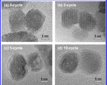
1/3 (10) I0total) I01st+ I02nd + I03rd + I04th+ ... + I0nth (11) Itotal) I1st+ I2nd + I3rd + I4th+ ... + Inth (12) Itotal I0 total ) I I0 × 1 + M + M2+ M3... + Mn-1 1 + M(0) + [M(0)]2+ [M(0)]3... + [M(0)]n-1 (13)the Al2O3shell layer; Figure 3b-d presents HRTEM images
of the crystalline TiO2particles prepared with Al2O3shell layers
using 2 to 10 cycles of ALD. All of the samples featured spherical-like, uniform, interconnected TiO2particles that were
ca. 20 nm in size. Table 1 lists the thicknesses of the Al2O3
overlayers prepared using 1 to 30 ALD cycles, as determined by TEM. Each listed thickness is the average value of 10 thickness measurements for the Al2O3overlayer. The thickness
values indicate a significant discrepancy in the deposition rates (nanometers/cycle) for the various reaction cycles. For a layer-by-layer growth process, a rate of deposition equivalent to 1 ML of the film per ALD cycle is ideal, that is,∼0.18 nm/cycle for Al2O3.23To better examine the distribution of the ALD Al2O3
deposit on the anatase nanoparticles, Figure 4 shows HRTEM images of the shell material deposited on a local area of the core particles before and after the first and the fifth deposition cycles. The HRTEM images clearly show that the distribution of the ALD Al2O3deposit is not uniform on the core particles,
indicating that the ALD deposition is via an island growth process.
IV. Applications of the C/S Model on the Nanoporous Electrode of DSSCs
Figure 5 shows the Ti 2p3/2XPS spectrum of the as-received
TiO2electrodes, indicating that the Ti 2p3/2core level of the
nanoporous TiO2electrodes was located at 458.9 eV, that is,
within the range from 458.8 to 459.4 eV reported for TiO2in
the literature.24Following ALD of the first Al
2O3overlayer, the
binding energy of the Ti 2p3/2 core level of the TiO2 layers
shifted by -0.5 to 458.4 eV; after 30 cycles, it shifted by +0.5 to 458.9 eV. These shifts in the Ti 2p3/2core levels indicate
that the Ti-O bond strength decreased within the 0.2 nm thick Al2O3 shell layer. The binding energy shift of the Ti 2p3/2
electron from -0.5 to +0.5 eV with increasing the thickness of the Al2O3overlayers can be partly attributed to the change
in the work function of the Al2O3-TiO2electrode. According
to our previous study, the work function (WF) of the electrode increases from 4.7 to 5.1 eV after the first ALD cycle, followed by decreasing with increasing the thickness of the Al2O3
overlayers (4.3 eV after 10 cycles of ALD).14The magnitude
and direction of the core level shifts observed in the XPS spectra
are in good agreement with the change of the WF with increasing the thickness of the Al2O3overlayer.
Figure 6 displays the Itotal/I
0totalratio measured by XPS as a
function of the thickness of the Al2O3shell layer on the TiO2
electrode. Each datum of the Itotal/I
0totalratio is the average value
of five measurements, with a deviation smaller than 3%. The solid curves are the theoretical curves, derived from the C/S model, for the Itotal/I
0totalratio as a function of the shell thickness
at various coverages (θ). When the number of ALD reaction cycles is smaller than 15, the measured Itotal/I
0totalratio falls on
the curves for θ< 1, revealing the presence of bare TiO2surface
areas. This is in agreement with the HRTEM images shown in Figure 4, which show an uneven distribution of the ALD Al2O3
deposits on the TiO2 nanoparticles and suggests that the
deposition of the ALD Al2O3film on TiO2nanoparticles is via
the island growth mode. For an island film growth, the growth and coalescence of deposited islands proceed during the ALD reaction, and a continuous island film will eventually develop. According to Figure 6, the measured Itotal/I
0total ratios for the
shell layers deposited by more than 15 reaction cycles fall on the curve for θ ) 1, indicating that the nanoporous TiO2
electrode was completely covered by the Al2O3shell layer; that
is, a continuous Al2O3film is formed.
Because XPS is very surface-sensitive with the probe depth smaller than 10 nm, a conclusive determination of the Itotal/I
0total
ratio through the 12 µm thick porous TiO2thin film electrode
simply by the XPS analysis is questionable. To clarify this issue, we used AES to analyze the cross section of a 22 µm thick nanoporous TiO2 layer with 10 cycles of the ALD Al2O3
overlayer. The AES analysis showed that the variation of the Al(KLL) signal was less than 1.8% through the cross section, suggesting that the ALD Al2O3layer was evenly deposited inside
the porous electrode. This result suggests that using XPS to study the Al2O3 coverage on the nanoporous electrodes of
DSSCs in terms of the C/S model is justified.
According to Figure 6, the ALD deposition with 1, 2, 5, and 10 cycles results in an Al2O3coverage of 0.25, 0.40, 0.71 and
0.83, respectively. However, the fitted coverage values are likely to have significant deviations from the true values because of several limitations bound to the application of the C/S model to the nanoporous DSSC electrodes. First, the C/S model assumes that the particle has a spherical shape, but the TiO2
nanoparticles in the DSSC electrodes exhibit various rounding shapes, which are far from a perfect spherical geometry. Second, the C/S model considers only those photoelectrons emitting from nanoparticles in the direction perpendicular to the sample surface. Although the line of sight of the input lens of the electron energy analyzer is perpendicular to the sample surface and the distance between the sample and the input aperture is considered to be infinitive compared with the nanoparticle diameter, detection of stray electrons emitting from other emission angles by the analyzer is inevitable. Third, the C/S model assumes a uniform island growth during the film deposition; that is, all islands developing on the substrate have the same thickness. However, this seems not to be true for the case of ALD Al2O3deposition on TiO2nanoparticles according
to the TEM analysis. Each datum shown in Figure 6 is the average value of 10 thickness measurements, and the average thickness will certainly deviate from the theoretical value for a particular coverage. Despite the above-described limitations of the C/S model, Figure 6 shows a reasonable trend in the coverage increase upon the increase in the number of ALD cycles. Therefore, we believe that the C/S model is applicable in the evaluation of the ALD Al2O3coverage.
Figure 3. TEM images of nanocrystalline TiO2core particles prepared (a) without an Al2O3shell layer, (b) with a two-cycle ALD Al2O3shell layer, (c) with a five-cycle ALD Al2O3shell layer, and (d) with a 10-cycle ALD Al2O3shell layer.
Figure 7 shows that the PCEs of the DSSCs changed upon varying the number of ALD reaction cycles of the Al2O3shell
layers. Each PCE datum in the figure is the average efficiency of 20 solar cells. Table 2 indicates that the efficiency increased initially by∼13% at an Al2O3layer thickness of ca. 0.2 nm,
but then it dropped dramatically to almost 0% upon further increasing the thickness. The initial increase of Jscat an∼0.2
nm thickness of the Al2O3layer may be attributed, in part, to
the reduction of recombination.3,6-9On the other hand, the drop
of the PCE is likely due to the tunneling effect,25 which will
exponentially decrease the current from dye to TiO2electrode
with increasing the thickness of the Al2O3overlayer, as indicated
by the short-circuit current (Jsc) listed in Table 2. The initial
increase in the value of the Vocis suggested to result from that
the high work function of the optimal ALD Al2O3 layer
thickness, as discussed above, provided a positive built-in potential (eVbi) at the Al2O3-TiO2interface.14Thus, increasing
the coverage of the optimal ALD Al2O3 overlayer on the
nanoporous TiO2 electrodes should enhance the PCE
pro-portionally.
The optimal ALD Al2O3layer thickness is 1 ML, or 0.2 nm,
which is considerably thinner than the reported 0.9-2.5 nm thicknesses of Al2O3films derived using sol-gel techniques.9,26
As discussed in previous studies,26,27the thickness of the sol-gel
TABLE 1: Thickness and Deposition Rate of the ALD Al2O3Shell Layers on TiO2Electrodes
sample: Al2O3shell layers 0-cycle 1-cycle 2-cycle 5-cycle 10-cycle 15-cycle 20-cycle 30-cycle thickness (nm)a
0 0.2 ( 0.1 0.5 ( 0.2 1 ( 0.4 1.9 ( 0.3 2.5 ( 0.4 2.8 ( 0.5 4.5 ( 0.5
deposition rate (nm/cycle) 0.2 ( 0.1 0.25 ( 0.1 0.2 ( 0.08 0.19 ( 0.03 0.17 ( 0.02 0.14 ( 0.02 0.15 ( 0.02
aThe thickness listed in the table is the average value of 10 TEM measurements at different locations of the C/S nanoparticle.
Figure 4. Enlarged TEM images show the TiO2 core particles (a) without an Al2O3shell layer, (b) with a one-cycle ALD Al2O3shell layer, and (c) with a five-cycle ALD Al2O3shell layer.
Figure 5. XPS spectra of the Ti 2p3/2peaks from the nanoporous TiO2 electrodes.
Figure 6. Coverages (θ) of Al2O3shell layers on TiO2electrodes, obtained from XPS analyses. The experimental data (crosses) match the corresponding theoretical curves from our C/S model.
Figure 7. Changes in the PCE and coverage, plotted with respect to
the number of ALD reaction cycles for Al2O3shell layers on TiO2 electrodes.
TABLE 2: Cell Performance of DSSCs Containing ALD Al2O3Overlayers of Various Thicknesses
Al2O3 thickness (nm) Voc(mV) Jsc (mA/cm2) FF (%) PCE (%) 0 737 ( 9 11.57 ( 0.43 66.9 ( 0.7 5.75 ( 0.22 0.2 (1-cycle) 765 ( 9 12.46 ( 0.38 68.7 ( 0.8 6.50 ( 0.15 0.5 (2-cycle) 744 ( 38 9.77 ( 0.21 68.6 ( 5.8 5.00 ( 0.16 1.0 (5-cycle) 796 ( 4 0.86 ( 0.11 67.9 ( 8.8 0.46 ( 0.12 1.9 (10-cycle) 764 ( 104 0.18 ( 0.01 37.2 ( 3.4 0.05 ( 0.01
films can only be altered with a resolution down to ∼1 nm; that is, the minimum achievable Al2O3thickness is ca. 1 nm.
The poorer infiltrating ability of the liquid precursors during sol-gel processing, generally resulting in an overestimation of the Al2O3thickness (i.e., the sol-gel films may accidentally be
thinner, falling into the desirable range of Al2O3layer
thick-nesses on electrode surfaces that are more difficult for the precursors to reach). Nevertheless, the ALD approach may not have much of an advantage over high-temperature sol-gel techniques due, in part, to the low coverage of ALD Al2O3
overlayers on nanoporous TiO2 electrodes at the optimal
overlayer thickness. Ideally, at the optimal thickness of the ALD Al2O3 overlayer, the PCE of the electrode is proportional to
the fractional coverage of the overlayer. According to Figure 7 and Table 2, the PCE is improved from 5.75% to 6.50% (i.e., an enhancement of 13.0%) if the nanoporous TiO2electrode is
coated by the Al2O3 overlayer with a coverage of 0.25.
Accordingly, as the coverage of the Al2O3overlayer approaches
1, the PCE of the electrode would have a PCE enhancement of more than 52%. However, under the present ALD deposition condition, the high PCE enhancement cannot be realized because of the island growth mode. If optimal ALD deposition condi-tions, such as the substrate temperature and precursor flow rate, can be successfully selected to increase the coverage for the first ALD deposition cycle, we believe that a better PCE for the ALD Al2O3-TiO2C/S DSSCs is achievable.
V. Conclusions
In this study, we established a C/S model, using XPS electron spectroscopy data, to calculate the surface coverage of shell layers. A relation of the XPS signal of a nanoporous substrate featuring interconnected nanoparticles with the fractional cover-age of the shell layer on the nanoparticles can be extracted from the model. We used the model to estimate the coverage of the ALD Al2O3 shell layer deposited on the nanoporous TiO2
electrodes of DSSCs as a function of the number of ALD reaction cycles. The coverage increased from 0.25 to 1.0 upon increasing the thickness of the Al2O3shell layers, indicating
that the ALD Al2O3deposition on the nanoporous electrode was
via the island growth mode. The PCE of the DSSCs was highest after the first ALD reaction cycle for the Al2O3shell layers. On
the basis of the coverage analysis, we predict that an
improve-ment in the PCE of ∼50% is obtainable when a single
monolayer of ALD Al2O3 (i.e., at the coverage of 1.0) is
deposited on the nanoporous TiO2electrode.
Acknowledgment. We thank Chia-Hua Lee (ITRI, Taiwan), Su-Jen Chen (ITRI, Taiwan), Iva Chan (ITRI, Taiwan), Peter Glink (www.editchem.com, U.S.A.), and the Microstructure and Characterization Laboratory (ITRI, Taiwan) for technical as-sistance and the Ministry of Economic Affairs of Taiwan, ROC, for generous financial assistance.
Supporting Information Available: The derivation on the total XPS/AES signal intensity of the core-shell (C/S) struc-tured nanoporous film with and without the shell layer is presented in the Supporting Information. This material is available free of charge via the Internet at http://pubs.acs.org. References and Notes
(1) Cui, Y.; Liu, L.; Li, B.; Zhou, X.; Xu, N. J. Phys. Chem. C 2010,
114, 2434.
(2) Antony, J.; Nutting, J.; Baer, D. R.; Meyer, D.; Sharma, A.; Qiang, Y. J. Nanomater. 2006, 54961.
(3) Zaban, A.; Chen, S. G.; Chappel, S.; Gregg, B. A. Chem. Commun.
2000, 2231.
(4) Kamat, P. V.; Schatz, G. C. J. Phys. Chem. C 2009, 113, 15473. (5) Rowley, J.; Meyer, G. J. J. Phys. Chem. C 2009, 113, 18444. (6) Lin, C.; Tsai, F. Y.; Lee, M. H.; Lee, C. H.; Tien, T. C.; Wang, L. P.; Tsai, S. Y. J. Mater. Chem. 2009, 19, 2999.
(7) Chen, S. G.; Chappel, S.; Diamant, Y.; Zaban, A. Chem. Mater.
2001, 13, 4629.
(8) Chappel, S.; Chen, S. G.; Zaban, A. Langmuir 2002, 18, 3336. (9) Palomares, E.; Clifford, J. N.; Haque, S. A.; Lutz, T.; Durrant, J. R.
J. Am. Chem. Soc. 2003, 125, 475.
(10) Zhang, X. T.; Liu, H. W.; Taguchi, T.; Meng, Q. B.; Sato, O.; Fujishima, A. Sol. Energy Mater. Sol. Cells 2004, 81, 197.
(11) Liu, Z.; Pan, K.; Liu, M.; Wang, M.; Lu, Q.; Li, J.; Bai, Y.; Li, T.
Electrochim. Acta 2005, 50, 2583.
(12) Guo, J.; She, C.; Lian, T. J. Phys. Chem. C 2007, 111, 8979. (13) Kim, W.; Tachikawa, T.; Majima, T.; Choi, W. J. Phys. Chem. C
2009, 113, 10603.
(14) Tien, T. C.; Pan, F. M.; Wang, L. P.; Lee, C. H.; Tung, Y. L.; Tsai, S. Y.; Lin, C.; Tsai, F. Y.; Chen, S. J. Nanotechnology 2009, 20, 305201.
(15) Hartlieb, P. J.; Roskowski, A.; Davis, R. F.; Plattow, W.; Nemanich, R. J. J. Appl. Phys. 2002, 91, 732.
(16) Sitar, Z.; Smith, L. L.; Davis, R. F. J. Cryst. Growth 1994, 141, 11.
(17) Gillet, J. N.; Meunier, M. J. Phys. Chem. B 2005, 109, 8733. (18) Martin, J. E.; Herzing, A. A.; Yan, W.; Li, X. Q.; Kobel, B. E.; Kiely, C. J.; Zhang, W. X. Langmuir 2008, 24, 4329.
(19) Renault, O.; Marlier, R.; Barrrett, N. T.; Martinez, E.; Baron, T.; Gely, M.; De Salvo, B. Surf. Interface Anal. 2006, 38, 486.
(20) Mohai, M.; Bertoti, I. Surf. Interface Anal. 2004, 36, 805. (21) Tanuma, S.; Powell, C. J.; Penn, D. R. Surf. Interface Anal. 1988,
11, 577.
(22) Zaban, A.; Ferrere, S.; Sprague, J.; Gregg, B. A. J. Phys. Chem. B
1997, 101, 55.
(23) Gosset, L. G.; Damlencourt, J. F.; Renault, O.; Rouchon, D.; Holliger, P.; Ermolieff, A.; Trimaille, I.; Ganem, J. J.; Martin, F.; Semeria, M. N. J. Non-Cryst. Solids 2002, 303, 17.
(24) Moulder, J. F.; Stickle, W. F.; Sobol, P. E.; Bomben, K. D.
Handbook of X-ray Photoelectron Spectroscopy; Perkin-Elmer Press: Eden
Prairie, MN, 1962; pp 45-73.
(25) Sze, S. M. Physics of Semiconductor DeVices; John Wiley & Sons: New York, 1983; Vol. 97.
(26) Palomares, E.; Clifford, J. N.; Haque, S. A.; Lutz, T.; Durrant, J. R.
Chem. Commun. 2002, 1464.
(27) Bandaranayake, K. M. P.; Indika Senevirathna, M. K.; Prasad Weligamuwa, P. M. G. M.; Tennakone, K. Coord. Chem. ReV. 2004, 248, 1277.