Energy-Efficient CMOS Large-Load Driver Circuit with the Complementary
Adiabatic/Bootstrap (CAB) Technique for Low-Power TFT-LCD System
Applications
G. Y. Liu, N. C. Wang and J. B. Kuo* Dept of Electrical Engineering, BL-528
National Taiwan University Taipei, Taiwan 106-17 Email:j.kuo@ieee.org
*J. B. Kuo is on leave from NTUEE, with SFU in Canada Abstract-This paper reports an energy-
efficient CMOS large-load driver circuit with the complementary adiabatic/bootstrap (CAB) technique for low-power TFT-LCD system applications. Using two differential inputs and via dual paths for bootstrap and energy recovery to VDD/ground, this CAB
load driver with an output load of 30pF and operating at 5V, provides a high-speed performance, consuming 60% less power as compared to the adiabatic/bootstrapped driver with single-path for bootstrap and energy recovery.
I. INTRODUCTION
Large-load driver circuit is an important component in a modern TFT-LCD system, where high speed and low power are the goals [1]. Bootstrap technique has been used in the low-voltage driver circuits to enhance speed performance of a VLSI system [2]-[4]. Energy efficiency of a large-load driver circuit is important in determining the power consumption of a TFT-LCD system. Adiabatic technique has been used to raise the energy efficiency of low-voltage VLSI circuits [5]. Recently, the adiabatic technique combining with the bootstrap technique to generate an energy efficient large-load driver circuit for low-voltage VLSI systems has been reported [6]. In this paper, an energy-efficient CMOS large-load driver circuit with the complementary adiabatic/bootstrap (CAB) technique via dual paths for bootstrap and energy recovery to VDD/ground, for low-power TFT-LCD system applications is described. In the following sections, this CMOS CAB load driver is described first, followed by performance and discussion.
II. CAB Load Driver
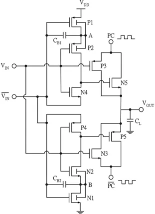
Fig. 1 shows the CMOS load driver using the complementary adiabatic/bootstrap (CAB)
Fig. 1. The CMOS CAB large-load driver circuit using the dual-path bootstrap/energy recovery technique.
technique via dual paths for bootstrap and energy recover to VDD/ground. As shown in the figure, P1, P2, P3, N4, N5, and the capacitor CB1 form the pull-up segment and N1, N2, N3, P4, P5, and the capacitor CB2 form the pull-down segment. In the pull-up segment, P1, P2, N4, N5 and CB1 are used to implement the bootstrap technique for enhancing the driving capability of N5 during the pull-up transient. By the same token, in the pull-down segment, N1, N2, P4, P5 and the capacitor CB2 are implemented to increase the driving capability of P5 using the bootstrap technique during the pull-down transient. Two differential inputs have been adopted in the circuits. Instead of
5258 0-7803-8834-8/05/$20.00 ©2005 IEEE.
Fig. 2. Equivalent circuits of the CMOS CAB load driver using the dual-path bootstrap/energy recovery technique when VIN is low (a) high (b).
the single path for bootstrap/energy recovery to VDD as in the previous approach [6], dual paths for energy recovery to VDD and ground have been adopted to increase the energy efficiency of this circuit.
The operation of this CMOS CAB load driver circuit is divided into two modes— when VINis low (1) and high (2). When VINis low (1), the pull-down segment is inactivated except that the bootstrap capacitor CB2 is charged with its left side to high and right side to 0V, since N1 is on. At the same time, in the pull-up segment the bootstrap capacitor CB1 is floating with its right side disconnected from VDD. In addition, the rest of the pull-up segment is
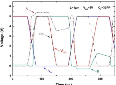
Fig. 3. Transient waveforms of the 5V CMOS CAB load driver using the dual-path bootstrap/energy recovery technique.
ready for (1) energy recovery and (2) output operations. When PC switches from high to low, it is the energy recovery operation for the pull-up segment. Energy recovery is done from the output load CL via N5. When PC is switching from low to high, it is the output operation period. During this period, the internal node A may exceed VDD as shown in Fig. 3 owing to the bootstrap capacitor CB1. Therefore a large driving current of N5 ensures a high pull-up switching speed at the final output.
The operations of energy recovery and output for the case when VIN is high are opposite to those described above for the case when VIN is low. When VIN is high, the pull-up segment is inactivated except the charge of the bootstrap capacitor CB1. In addition, energy recovery and output operations are done for the pull-down segment depending on PC*. When PC* turns from low to high, energy recovery is done from the output node via P5. When PC* turns low, it is the output period for the pull-down segment, where internal B may go under 0V due to the bootstrap capacitor CB2, which enhances the driving capability of P5 such that the pull-down speed of the output node could be enhanced. Owing to the implementation of the CAB technique via the dual paths of bootstrap/energy recovery to VDD and ground, the energy efficiency and the 5259
speed of this large-load driver have been enhanced.
III. PERFORMANCE
In order to assess the performance of this CMOS CAB large-load driver circuit with the dual-path energy recovery/bootstrap technique, a test circuit using a 5V power supply voltage with a capacitive load of 30pF at the output node, based on a 0.35µm CMOS technology has been designed. The channel length of all devices in the circuit is 1µm. Bootstrap capacitor CB1/CB2 of 0.5pF/0.8pF has been used. Fig. 3 shows the transient waveforms of this load driver circuit at 5V. As shown in the figure, owing to the function of the bootstrap capacitors CB1/CB2, the internal node A/B may
Fig. 4. Consumed energy of the 5V CMOS CAB large-load driver using the dual-path adiabatic/ bootstrap technique.
be higher/lower than 5V/0V. Thus the final output can be pulled to high/low at a high speed owing to the enhanced driving capability of N5/P5.
Fig. 4 shows the consumed energy of this 5V CMOS CAB large-load driver using the dual-path adiabatic/bootstrap technique operating at PC of 8MHz. Also shown in the figure are the results for the load drivers using the single-path adiabatic/bootstrap approach [6]. Note that P block means the driver with the pull-up segment only and N block implies the
one with the pull-down segment only. As shown in the figure, the CMOS CAB load driver with the dual-path bootstrap/energy recovery technique indicates a 60.3%/82% reduction in the power consumption as compared to the one with N block/P block using the single-path bootstrap/energy recovery technique [6]. From this figure, the CMOS CAB load driver with the dual-path bootstrap/energy recovery technique is effective in raising the energy efficiency of the circuit.
IV.DISCUSSION
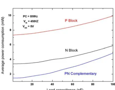
Fig. 5. Average power consumption versus load capacitance of the 5V CMOS CAB load driver using the dual-path bootstrap/ energy recovery techniques
This CMOS CAB load driver using the dual-path bootstrap/energy recovery technique is especially advantageous when the load is large. Fig. 5 shows the average power consumption versus load capacitance of the CMOS CAB load driver using the dual-path bootstrap/energy recovery technique at the clock frequency of 8MHz. Also shown in the figure are the results for the load driver using the single-path adiabatic/bootstrap approach [6]. As shown in the figure, at a load capacitance of 100pF, the CMOS CAB load driver using the dual-path bootstrap/energy
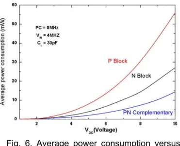
Fig. 6. Average power consumption versus power supply voltage of the CMOS CAB load driver using the dual-path bootstrap/energy recovery technique.
recovery technique offers a 16%/50% reduction in the average power consumption as compared to the N block/P block using the single-path bootstrap/energy recovery technique [6].
Fig. 6 shows the average power consumption versus power supply voltage of the CMOS CAB load driver using the dual-path bootstrap/energy recovery technique with a load capacitance of 30pF at the clock frequency of 8MHz. As shown in the figure, at the power supply voltage of 10V, the CMOS load driver with the dual-path bootstrap/ energy recovery technique offers a reduction of 42%/73% in the average power consumption as compared to the N block/P block one using the single-path adiabatic/ bootstrap technique. Consequently, the CMOS CAB load driver using the adiabatic/bootstrap techniques is effective in high speed and energy efficiency.
CONCLUSION
In this paper, an energy-efficient CMOS large load driver circuit with the complementary adiabatic/bootstrap (CAB) technique for low-power TFT-LCD system applications has been reported. Using two differential inputs and via dual paths for bootstrap and energy recovery to VDD/ground, this CAB load driver with an output load of
30pF and operating at 5V, provides a high-speed performance, consuming 60% less power as compared to the adiabatic/ bootstrapped driver with single-path for bootstrap and energy recovery.
ACKNOWLEDGMENT
This project is supported under R.O. C. National Science Council Grant No. 83-2215-E002-020.
REFERENCES
[1] T. Itakura, H. Minamizaki, T. Saito, T. Kuroda, “A 402-output TFT-LCD Driver IC with Power Control Based on the Number of Color Selected,” IEEE J. Solid-State Circuits, Vol. 38, No. 3, pp. 503-510, March 2003.
[2] C. F. Law, K. S. Yeo, and R. S. Samir, “Sub-1V Bootstrapped CMOS Driver for Giga-Scale-Integration Era,” Elec. Lett., Vol. 35, No. 5, pp. 392-393, 1999.
[3] K. S. Yeo, J. G. Ma, M. A. Do, “Ultra-Low-Voltage Bootstrapped CMOS Driver for High Performance Applications,” Elec. Lett., Vol. 36, No. 8, pp. 706-707, 2000.
[4] J. H. Lou and J. B. Kuo, “A 1.5V Full-Swing Bootstrapped CMOS Large Capacitive-Load Driver Circuit Suitable for Low-Voltage CMOS VLSI,” IEEE J. Solid-State
Circuits, Vol. 32, No. 1, pp. 119-121, 1997.
[5] Y. Zhang, H. H. Chen, and J. B. Kuo, “0.8V CMOS Adiabatic Differential Switch Logic Circuit Using Bootstrap Techniques for Low-Voltage Low-Power VLSI,” Elec. Lett., Vol. 38, No. 24, pp. 1497-1499, 2002. [6] H. P. Chen and J. B. Kuo, “A Low-Voltage
CMOS Load Driver with the Adiabatic and Bootstrap Techniques for Low-Power System Applications,” MWSCAS Proc., Hiroshima, July 2004.