行政院國家科學委員會專題研究計畫 成果報告
針對 3D 整合之電子設計自動化技術開發--子計畫四:立體
堆疊晶片與系統級構裝之設計最佳化研究(2/2)
研究成果報告(完整版)
計 畫 類 別 : 整合型 計 畫 編 號 : NSC 99-2220-E-009-038- 執 行 期 間 : 99 年 08 月 01 日至 100 年 07 月 31 日 執 行 單 位 : 國立交通大學電子工程學系及電子研究所 計 畫 主 持 人 : 陳宏明 計畫參與人員: 碩士班研究生-兼任助理人員:吳永證 碩士班研究生-兼任助理人員:張業琦 碩士班研究生-兼任助理人員:翁逸芃 碩士班研究生-兼任助理人員:羅婉婷 大專生-兼任助理人員:黃川嘉 大專生-兼任助理人員:陳孟伶 大專生-兼任助理人員:林子恆 博士班研究生-兼任助理人員:李杰叡 博士班研究生-兼任助理人員:秦敬雨 博士班研究生-兼任助理人員:劉時穎 博士班研究生-兼任助理人員:王俊凱 博士班研究生-兼任助理人員:潘柏丞 公 開 資 訊 : 本計畫可公開查詢中 華 民 國 100 年 10 月 31 日
中文摘要: 超大型積體電路設計日益複雜,加上奈米效應使得晶片與封裝 的設計變得更加困難,因此電子設計自動化產品也必需不斷的 進步以符合時代的需求。在先進設計與堆疊晶片設計中,覆晶 封裝(flip-chip)具有低設計成本的優點,但通常需要利用重新分 配層(Redistribution layer, RDL)繞線來連接 IO 訊號線。有時 RDL 繞線非常的擁擠,即使用人工繞線仍無法與一層中完成。 在此報告中,我們提出虛擬單層(pseudo single-layer)繞線的概 念。此方法可以考慮封裝設計以及堆疊晶片的設計問題。利用 啟發式演算法,將問題轉換成 channel 繞線的形式,極小化繞 線所需的面積,並達到百分之百的繞線完成度。與手動繞線、 商業用工具等的結果作比較,我們的方法應用在實際工業設計 上相當有效。 英文摘要:
針對3D整合之電子設計自動化技術開發
子計畫四:立體堆疊晶片與系統級構裝之設計最佳化研究(2/2) 3D-SIC and 3D-SIP Design Planning
計畫編號:NSC 99-2220-E-009-038 執行期間:99 年 8 月 1 日 至 100 年 7 月 31 日 計畫主持人:陳宏明 一、中文摘要 超大型積體電路設計日益複雜,加上奈米效應使得晶片與封裝的設計變得更 加困難,因此電子設計自動化產品也必需不斷的進步以符合時代的需求。在先進 設計與堆疊晶片設計中,覆晶封裝(flip-chip)具有低設計成本的優點,但通常 需要利用重新分配層(Redistribution layer, RDL)繞線來連接 IO 訊號線。有時 RDL 繞線非常的擁擠,即使用人工繞線仍無法與一層中完成。在此報告中,我們 提出虛擬單層(pseudo single-layer)繞線的概念。此方法可以考慮封裝設計以 及堆疊晶片的設計問題。利用啟發式演算法,將問題轉換成 channel 繞線的形式, 極小化繞線所需的面積,並達到百分之百的繞線完成度。與手動繞線、商業用工 具等的結果作比較,我們的方法應用在實際工業設計上相當有效。 關鍵詞:三維度積體電路;封裝設計;flip-chip 繞線 二、英文摘要
Due to the advantage of flip-chip design in power distribution but controversial peripheral IO placement for lower design cost, redistribution layer (RDL) is usually used for such interconnection. Sometimes RDL is so congested that the capacity for routing is insufficient. Routing therefore cannot be completed within a single layer even for manual routing. Although [2] proposed a routing algorithm that uses two layers of RDLs, but in practice the required routing area is a little more than one layer. We overcome this problem by adopting the concept of pseudo single-layer. With the heuristics for routing on mapped channels and observations on staggered pins to
relieve vertical constraints, the area of 2-layer routing can be minimized and the routability is 100%. Comparisons of routing results between manual design, the commercial tool, and the proposed method are presented. We have shown the effectiveness on a real industrial case: it originally required fully manual design, the proposed method can finish RDL routing automatically and effectively.
三、研究計畫之背景及目的
A. 背景
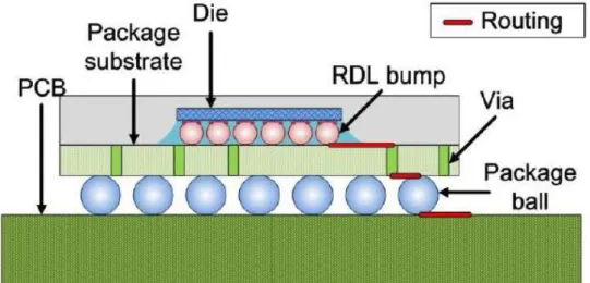
As the demand for more input/output (IO) increases, traditional packaging method, wire bonding is not effective to support thousands of IOs. Flip-chip assembly is now commonly used because it reduces chip area while supporting more IOs. It can also greatly reduce inductance, allow highspeed signals, and carry heat better. For high IO count chips, a general purpose packaging method is flip-chip ball grid array (FCBGA). Among all packaging technologies, FCBGA is nowadays the best choice in electrical performance and IO count for high-end chips. RDL is the interface between chip and package for flipchip assembly (Fig. 1). An RDL is an extra metal layer of wiring on top of core metals which makes the IO pads of die available in other locations. It enables bonding out IO pads to other locations such as bump pads. Bumps are usually placed in a grid pattern and each is molded with two pads, one on the top, one on the bottom, attached to RDL and package substrate respectively. RDL therefore serves as the layer connecting IO pads and bump pads.
Fig. 1. The cross section in flip-flop: signal trace traveling through three interfaces including RDLs.
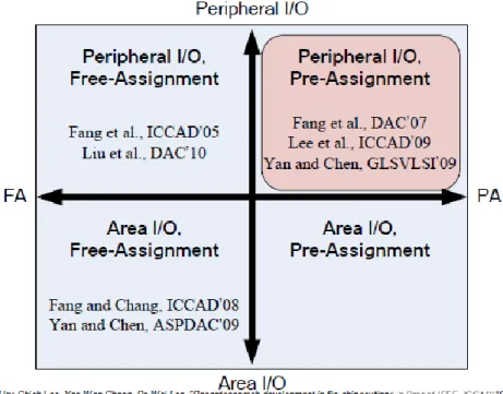
Fig. 2. Research map of previous works. Free-assignment (FA) and preassignment (PA) are 2 methods for pad assignment. Peripheral-IO (PIO) and area-IO (AIO) are 2 flip-chip structures.
In this work, we focus on PIO-PA problem.
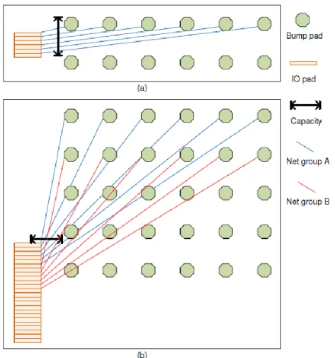
Previous works can be classified into 4 types based on the flip-chip structures and pad assignment methods. A research map proposed by [3] is shown in Fig. 2. Two pad assignment methods, free-assignment (FA) and pre-assignment (PA), represent whether the mapping between bump pads and IO pads is given as input. For FA problems, each IO pad is free to assign to any bump pad, so assignment is considered together with routing. For PA problems, each IO pad must connect with the specified bump pad, therefore solving complex crossings is the focus. Consequently, PA problems are more difficult than FA ones but more convenient for designers. Two flip-chip structures, area-IO (AIO) and peripheral-IO (PIO), represent patterns of IO placement. AIO and PIO problems are to place IOs in the central area and on the peripheral of die respectively. PIO is more popular today mainly because of its simplicity and low design cost, even though AIO is theoretically better in performance. An example of PIO is shown in Fig. 3.
PIO-FA problems are solved by [4], [5] using network flow algorithms such as minimum cost maximum flow (MCMF). PIO-PA problems are solved by [6], [8] using integer linear programming (ILP). Under the routing model of [6], [7], their ILP
method guarantees an optimal solution. AIO-FA problems considering signal skew are solved by [9], [10] using MCMF. Recently, the problems regarding unified AIO, which means an RDL containing both AIO-FA and AIO-PA problems, are solved by [11]. In this work, we focus on problem of PA and PIO, related previous works are listed in the first quadrant of Fig. 2.
B. 目的
All aforementioned previous works focus on single-layer routing. They restrict routes within one metal layer, on which every net must be routed. The common objective is wire-length minimization. Their optimization schemes are done under a prerequisite that routability is 100%. They have proved to be very successful for each type of RDL routing problems, providing that a solution exists within single layer. However, one layer routing is not practical in today’s flip-chip design.
In this project, we focus on RDL routing with congestion, which is difficult to route it within single layer. Our goal and contributions are described as follows: The proposed RDL router targets at congested cases where 100% routability is not easy to achieve within single layer. The concept of pseudo single-layer routing is introduced. It is to borrow a small part of area, which is less critical in performance, from another exsiting metal layer. With some techniques such as regional layer allocation and assignment of movable pins, the problem can be solved by classical channel routing algorithms. Our approaches can achieve 100% routability and minimize the area for 2-layer routing on a real industrial case.
四、研究方法
Section I shows our setup in pseudo single layer of RDL and problem formulation. Section II shows how we generate our “channels” in RDL routing, and Section II shows our adoption of channel routing via staggered/movable pins. Section IV reports our result on a real industrial case, and section V is the conclusion.
I. PRACTICAL RDL ROUTING
A. Routing on Pseudo Single-Layer
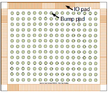
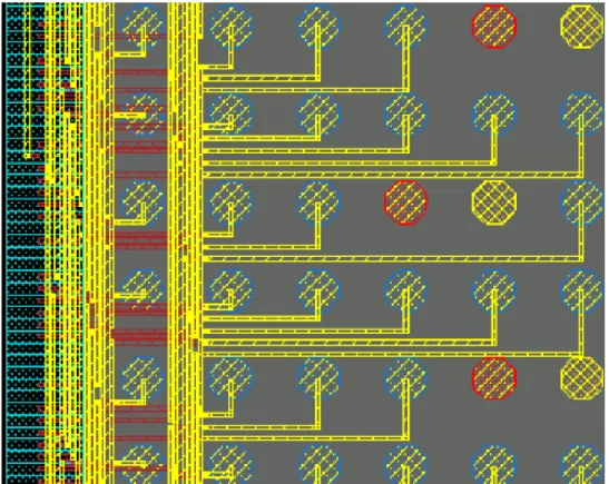
Both RDL routing and bump assignment are additional implementation tasks for design houses to migrate designs from wire bonding to flip-chip. Bump assignment is to assign each bump to a specific IO pad. Since IO pads are put on the periphery of die for most designs, the flylines and signal routing look like nets escaping from center to boundary of chip. For our designs under consideration, there are two layers of RDL. Metal10 (M10) and metal9 (M9) are used to route all signal nets and to implement power/ground (PG) mesh and power routing respectively. Usually the number of signal nets to be routed is generally huge for RDL. Bump pads are large in area and are treated as obstacles in routing stage. An example of real scale design is shown in Fig. 3.
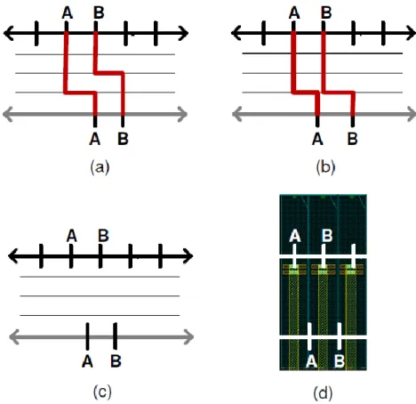
Fig. 4(a) shows an example of congested RDL, where 6 nets, netA, netB, ..., netE, are shown in flylines. Such designs are so congested that 100% routability is not achieved within single layer (ex: M10), so we must consider two trivial solutions. One is to increase the area of RDL (ex: M10), which is equivalent to increasing the die-size, as shown in Fig. 4(b). Another is to add an extra layer of RDL (ex: M11), as shown in Fig. 4(c). However, neither of the solutions mentioned is acceptable for cost concern.
We hereby introduce the concept called Pseudo Single−Layer Routing. It is to borrow a small portion of area from another existing metal layer (ex: M9). This is practical and cost-effective provided that the area is less critical in performance. In Fig. 4(d), some area of M9 (the pink area) is borrowed to complete routing. Here we assume that the area between a boundary track (the dotted grey line) and the border of die is used to assist routing. The idea of pseudo single-layer routing avoids cost problems and realizes congested routing. While previous works focus on pure single-layer routing, the concept of pseudo single-layer uses 2-layer routing within a small portion of area. This is applicable to RDL because of the following reason. M9 is traditionally used to connect PG from IO pads to core. Some different styles of PG nets such as rings, stripes, and meshes are therefore designed. The most important function of M9 is to evenly distribute power to every logic gate in the core. So the
peripheral area of M9 is relatively less important than the central area. This is the key observation which enables signal nets to share peripheral area of M9 with PG nets.
Fig. 3. Top view of RDL. There are bump pads in a grid pattern and IO pads on the periphery.
Fig. 4. Solutions for congested RDL routing. An RDL is congested if it has many signal IO nets to be routed and a single RDL cannot provide sufficient capacity for routing. In (a), two trivial solutions are shown in (b) and (c). Solution (b) increases the area of RDL (M10), while
solution (c) adds an extra RDL (M11). We propose another solution, pseudo single-layer, which is a compromise in-between. It is to borrow a small region of an existing RDL (M9), as
B. Problem Definition
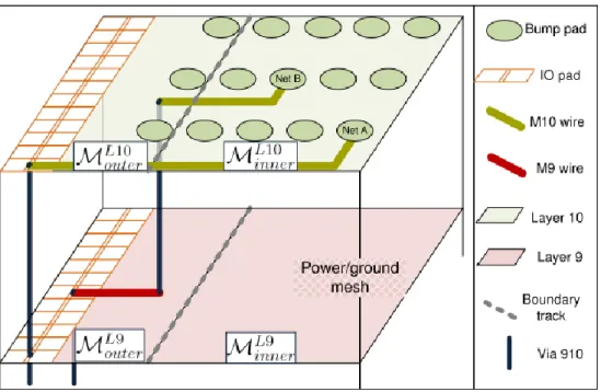
The problem of RDL routing is to connect net Ni between the bump pad Bi and the input/output pad IOi. First and second RDLs are M9 and M10 respectively, as shown in Fig. 5. We name the area as inner/outer region with respect to the boundary track. Regarding to layers and inner/outer region, the whole RDL is partitioned into four sectors: ML10outer, ML10inner, ML9outer, and ML9inner.
Definition of Terms:
• Routable region (pseudo single-layer): ML10outer ∪ ML10inner ∪ ML9outer
• Outer region: ML10
outer ∪ ML9outer
• Inner region: ML10
inner ∪ ML9inner
The pseudo single-layer RDL routing problem is to physically connect Bi and IOi of net Ni in routable region and to minimize the area of inner region. This also means that the boundary track is not fixed; the solution of this problem is to determine the location of boundary track. The problem formulation is thus as follows:
Input:(Fig. 6)
• Given physical locations of bump pads Bi and IO pads IOi • Given Bi − IOi mapping of net Ni
Output: • Single-layer routing in ML10 inner • Two-layer routing in ML10 outer ∪ ML9outer Objective:
• Minimize the area of outer region (preserve the integrity of PG routing)
The whole area of RDL is divided into four sectors by two diagonals: west, north, east, and south. In the following descriptions, we focus on west region only. In our implementation, north, east, and south regions are counterclockwise rotated 90, 180, 270 degrees respectively. There are no sector boundary nets to be processed.
Fig. 5. Problem definition. First and second RDLs are layer 9 and layer 10 respectively.
Fig. 6. Physical locations of bump pads and IO pads are given. The bump-IO mapping is shown in flylines.
II. CHANNELS FOR CONGESTED RDL ROUTING
The modeling of routable region is presented here. Firstly, some analyses of the region are derived. Secondly, an abstraction from physical layouts to tracks and pins is presented. Lastly, to efficiently utilize routable spaces, regional layer allocation is proposed.
A. Constraints and Considerations in Manual RDL Routing
Here we address the constraints and considerations learned from manual routes and the designs under consideration. The example in Fig.7 is a real situation from industrial experience. There are few crossings due to a well devised bump-IO assignment. There is sufficient capacity for horizontal wires because the row can support larger capacity, say six wires. In Fig.7(a), all nets can be routed from bump pads to IO pads in one row without any difficulty. However, capacity for vertical wires is insufficient because 24 nets (4 rows × 6 bumps per row) travel through the horizontal cut line. In Fig.7(b), only 12 flylines (out of 24 nets) are plotted. The capacity is small that there is no room for 24 vertical wires.
Fig. 7. Capacity constraints for horizontal wires (a) and vertical wires (b).
From the example in Fig. 5, we can observe that there is only limited area (horizontal channels) for routing in M10 (ML10outer Union ML10inner). For instance,
nets to route within its own horizontal channel, the route from BA has no choice but
goes left directly to connect IO. What we learn is that it is allowed to share the peripheral region (ML9outer), but we need to leave some spaces unused for PG IOs to
route to inner region of M9 to connect with PG mesh. Due to this implicit constraint, we use the following techniques to help us.
B. Defining Routing “Channels”
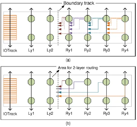
In west region, bump pads are on the right and IO pads are on the left (Fig. 8), the placement of IO pads forms a vertical column (IO track). Wires of the inner-most (rightmost) bumps generally escape horizontally to reach their corresponding IO pads. We propose a pin-track model to simplify the layout representation of RDL. This will lead us to the application of channel routing algorithm.
We assume that wires can go either horizontally or vertically, although 45-degree wires are usually used in RDL. We define horizontal direction as x-axis and vertical direction as y-axis. Then a track is a vertical line where x-coordinate is fixed, and a pin is a point on a track. The x-coordinate of IO track is the x-coordinate for every IO pad because IO pads are assumed to be in a column and uniform in size. In Fig. 8, there are IO track, boundary track, and 6 bump tracks (Ly1, Ly2, Ry1, Ry2, Ry3, Ry4). Nets must travel through tracks on their left side to reach IO pads. Pins are then the points where wires travel across tracks.
Fig. 8. Modeling of layout. There are IO track, boundary track, and 6 bump tracks (Ly1, Ly2, Ry1, Ry2, Ry3, Ry4). In (a), on the right of boundary track, each bump track can have some possible paths (dotted lines) to route to boundary track, and one of paths is routed (solid lines).
In (b), routes are extended onto the boundary track, the area for 2-layer routing (ML10outer
Union ML9outer) contains two bump tracks and is enclosed by IO track and boundary track.
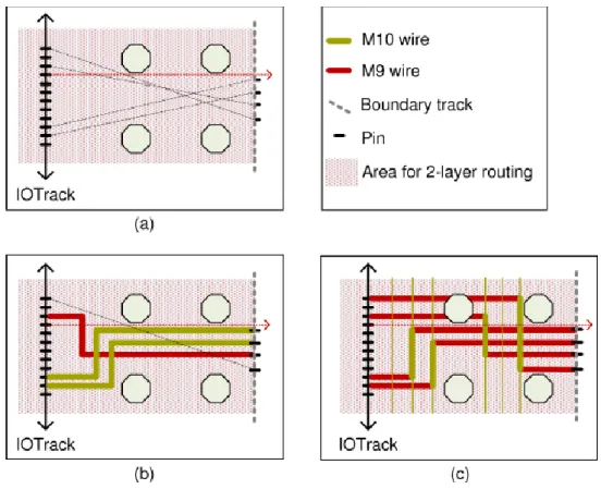
C. Regional Layer Allocation for Effective Capacity Utilization
In outer region, two layers are available for signal routing. To effectively utilize routing capacity, two solutions for routing resource allocation are illustrated in Fig. 9. Regional layer allocation is proposed as follows. One layer is for horizontal wires and the other one is for vertical wires. Horizontal wires are used to connect from IO pads to the assigned track. They cannot be blocked by any obstacle. Thus, the allocation is that horizontal wires are routed in M9 (Fig. 9(c)) based on the observation that M10 contains full of bumps. Another advantage of this allocation is that PG wires go horizontally to central/inner RDL using M9. This allocation guarantees to leave some spaces for PG wires. Vertical wires are therefore used to connect two pins on a track. Note that layer assignment (Fig. 9(b)) has some drawbacks and limitations due to the inflexibility. This technique will be performed along with the following channel
routing application.
Fig. 9. Solutions for routing resource allocation. The example in (a) contains 4 nets. Layer assignment for nets, as shown in (b), has some drawbacks and limitations. We propose
regional layer allocation to avoid the drawbacks, as shown in (c).
III. “CHANNEL” ROUTING WITH STAGGERED “PINS”
The proposed routing algorithm has three steps: Step1 is to route a net from bump pad to a pin; Step2 is to decide which track to use; Step3 is to route from IO pad to the pin.
A. Channel Routing on Mapped Routing Channels
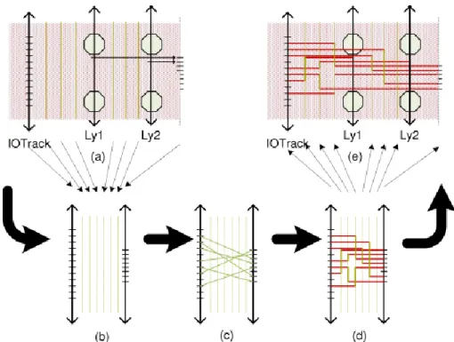
Fig. 10 shows the abstraction from tracks to channel routing, and the corresponding results. First, all bump pins are projected to one track called virtual track. Then we apply classical left-edge algorithm (LEA) on the channel between IO track and the virtual track. Then minimum number of required tracks can be obtained. The results are mapped onto layout once the results are obtained (Fig. 10(e)).
Fig. 10. Channel routing on mapped channels. Abstraction from physical layout to channel routing is shown in (a). For the example in (b), the results shown in (c) are obtained by applying LEA, and physically routed in (d). Then they are mapped to real solution in RDLs in
(e).
B. Assignment of Movable Pins on Pin-Tracks
In Step1, we have that pins are movable along track within certain distance. In Fig. 11 (view the channel in Fig. 10(b) rotating 90 degree), pinA is movable if capacity
for the bottom track is sufficient. We can assign locations of the pins once they are movable. The impact of locations of pins is beneficial. As shown in Fig. 11(a), minimum number of tracks for this case is two since the pin of B on the top track (IO-pin) and the pin of A on the bottom track (bump-pin) have vertical constraint. However, if bump-pin A is moved to its left, then minimum number of tracks is reduced to one, as shown in Fig. 11(b). So the assignment of movable pins can affect the number of required tracks. If they can be well assigned, vertical constraints can also be greatly reduced.
Based on some observations from design parameters, the idea of staggered pins can be applied to accommodate staggered/movable pins. Since there is enough capacity to place one horizontal wire at each border of IO pads, bump-pins can be staggered from IO-pins, as shown in Fig. 11(c). Besides, once the pins are staggered,
vertical constraints can be eliminated.
Fig. 11. Impact of pin locations. A vertical constraint (VC) exists between NA and NB in (a). It can be relieved by a slight shift of pinA, as shown in (b). The idea of staggered pins is to stagger all pins, as in (c), on each track so that no VC exists. In
real scale layout, this idea is implementable. As shown in in (d), when pins on IO-track locate at the center of the pads, the space allows virtual pins to staggered
from IO-pins.
IV. VERIFYING THE EFFECTIVENESS
The proposed algorithms are performed on a real and big industrial case. The whole chip is divided into four sectors: W, N, E, and S. Each sector contains more than a hundred signal bumps.
We implement the algorithm in tool command language Tcl. The data are fetched from the design in Encounter Digital Implementation (EDI) during data preparation. This pre-processing generates the input of our algorithm. For each sector, our algorithm can generate the results and dump scripts of commands in less than 5 seconds. By sourcing these scripts in EDI, wires are physical routed. This can also be
obtained by any pin-to-pin router since all the pin positions are allocated. All results are clean in design rule checking (DRC). The routing results are shown in Fig. 12 and Fig. 13, and summarized in Table I. Due to non-disclosure agreement (NDA), only partial results are shown. Without painful manual routing, we can obtain acceptable results in almost no time.
TABLE I
THE SUMMARY OF ROUTING RESULTS.
Fig. 13. Our routes.
V. CONCLUSIONS
We introduce a methodology for RDL routing on pseudo single-layer. The designs under consideration are so congested that even manual routing cannot find solutions within singlelayer. To deal with congested RDL, the concept of pseudo single-layer is proposed. We have shown that it provides a feasible solution other than adding an extra metal layer or increasing the die-size.
We address regional layer allocation, assignment of movable pins, and layout abstraction. These techniques transform the RDL routing problem into classical channel routing problem. By simply applying left-edge algorithm (LEA), 100% wires are routed and the area of 2-layer routing is minimized. Comparisons of routing results from manual design, commercial tool, and the proposed method are provided.
五、參考文獻
[1] P. Dehkordi and D. Bouldin, “Design for packageability-the impact of bonding technology on the size and layout of VLSI dies,” in Proceedings Multi-Chip
Module Conference, pp. 153-159, 1993.
[2] J.-W. Fang and Y.-W. Chang, “Area-I/O flip-chip routing for chip package co-design,” in Proc. IEEE/ACM international Conference on Computer-Aided
Design, pp. 518-521, 2008.
[3] H.-C. Lee, Y.-W. Chang, and P.-W. Lee, “Recent research development in flip-chip routing,” in Proc. IEEE/ACM international Conference on
Computer-Aided Design, pp. 404-410, 2010.
[4] J.-W. Fang, I-Jye Lin, Y.-W. Chang, and J.-H. Wang, “A network-flow based RDL routing Algorithms for flip-chip design,” in IEEE Trans. on
Computer-Aided Design of integrated Circuits and Systems, vol. 26, no. 8, pp.
1417-1429, Aug. 2007.
[5] J.-W. Fang, I-J. Lin, P.-H. Yuh, Y.-W. Chang, and J.-H. Wang, “A routing algorithm for flip-chip design,” in Proc. IEEE/ACM international Conference on
Computer-Aided Design, pp. 753-758, Nov. 2005.
[6] J.-W. Fang, C.-H. Hsu, and Y.-W. Chang, “An integer linear programming based routing algorithm for flip-chip design,” in Proc. ACM/IEEE Design Automation
Conference, pp. 606-611, June 2007.
[7] P.-W. Lee, C.-W. Lin, Y.-W. Chang, C.-F. Shen, and W.-C. Tseng. “An efficient pre-assignment routing algorithm for flip-chip designs,” in IEEE/ACM
international Conference on Computer-Aided Design, pp. 239-244, Nov. 2009.
[8] J.-W. Fang, C.-H. Hsu, and Y.-W. Chang, “An
integer-linear-programming-based Routing algorithm for flip-chip designs,” in
IEEE Trans. on Computer-Aided Design of integrated Circuits and Systems, vol.
28, no. 1, pp. 98-110, 2009.
[9] J.-W. Fang and Y.-W. Chang, “Area-I/O flip-chip routing for chip package co-design considering signal skews,” in IEEE Trans. on Computer-Aided Design
of integrated Circuits and Systems, vol. 29, no. 5, pp. 711-721, 2010.
[10] K.-S. Lin, H.-W. Hsu, R.-J. Lee, and H.-M. Chen, “Area-I/O RDL routing for chip-package codesign considering regional assignment,” in Proc. IEEE
Electrical Design of Advanced Packaging & Systems Symposium, pp. 1-4, 2010.
[11] J.-W. Fang, M.D.F. Wong, and Y.-W. Chang, “Flip-chip routing with unified area-I/O pad assignments for package-board co-design,” in Proc. ACM/IEEE
國科會補助計畫衍生研發成果推廣資料表
日期:2011/10/31國科會補助計畫
計畫名稱: 子計畫四:立體堆疊晶片與系統級構裝之設計最佳化研究(2/2) 計畫主持人: 陳宏明 計畫編號: 99-2220-E-009-038- 學門領域: 晶片科技計畫--整合型學術研究 計畫無研發成果推廣資料
99 年度專題研究計畫研究成果彙整表
計畫主持人:陳宏明 計畫編號:99-2220-E-009-038- 計畫名稱:針對 3D 整合之電子設計自動化技術開發--子計畫四:立體堆疊晶片與系統級構裝之設計最 佳化研究(2/2) 量化 成果項目 實際已達成 數(被接受 或已發表) 預期總達成 數(含實際已 達成數) 本計畫實 際貢獻百 分比 單位 備 註 ( 質 化 說 明:如 數 個 計 畫 共 同 成 果、成 果 列 為 該 期 刊 之 封 面 故 事 ... 等) 期刊論文 0 0 100% 研究報告/技術報告 0 0 100% 研討會論文 0 0 100% 篇 論文著作 專書 0 0 100% 申請中件數 0 0 100% 專利 已獲得件數 0 0 100% 件 件數 0 0 100% 件 技術移轉 權利金 0 0 100% 千元 碩士生 4 4 100% 博士生 5 5 100% 博士後研究員 0 0 100% 國內 參與計畫人力 (本國籍) 專任助理 0 0 100% 人次 期刊論文 4 4 100% 研究報告/技術報告 0 0 100% 研討會論文 8 8 100% 篇 論文著作 專書 0 0 100% 章/本 申請中件數 0 0 100% 專利 已獲得件數 0 0 100% 件 件數 0 0 100% 件 技術移轉 權利金 0 0 100% 千元 碩士生 0 0 100% 博士生 0 0 100% 博士後研究員 0 0 100% 國外 參與計畫人力 (外國籍) 專任助理 0 0 100% 人次其他成果