國 立 交 通 大 學
電子工程學系 電子研究所
碩士論文
鈷矽氧化奈米點在非揮發性憶體應用之研究
Study on the Application of Co-Si-O Nanocrystal for
Nonvolatile Memory
研 究 生:薛培堃
指導教授:張俊彥 院士
鈷矽氧化奈米點在非揮發性憶體應用之研究
Study on the Application of Co-Si-O Nanocrystal for
Nonvolatile Memory
研 究 生:薛培堃 Student:Shueh Pei-Kun
指導教授:張俊彥 院士 Advisor:Dr. Chun-Yen Chang
國 立 交 通 大 學
電子工程學系 電子研究所
碩 士 論 文
A Thesis
Submitted to Department of Electronics Engineering and
Institute of Electronics
College of Electrical and Computer Engineering
Nation Chiao Tung University
In Partial Fulfillment of Requirements
For the Degree of
Master
in
Electronics Engineering
July 2008
Hsinchu, Taiwan, Republic of China
鈷矽氧化奈米點在非揮發性
記憶體應用之研究
研究生: 薛培堃 指導教授 : 張俊彥 院士
國立交通大學
電子工程學系 電子研究所
摘要
近年來,數位生活在台灣電子工業市場扮演了舉足輕重的角色,數位電子產品 的應用已經受到廣大的青睞,像是數位相機、筆記型攜帶式、攜帶隨身聽MP3或CD、 信用卡晶片,攜帶型USB記憶體或記憶卡和日常生活會用到的PDA、GPS 等等。這些 個人式電子產品的發展則基於非揮發性記憶體元件的低功率消耗和可攜式。傳統的 非揮發性記憶體是利用複晶矽浮停閘(floating gate)作為載子儲存的單元,而在元 件尺寸持續微縮下,該結構將面臨一些瓶頸。當電子從通道注入浮停閘儲存層,記 憶體元件將會受到儲存載子影響它本身存在電場的影響,造成起始電壓的漂移。我 們可將受浮停閘改變的起始電壓定義為1與O。然而,因為這種浮停閘結構為整層的 半導體薄膜,在電子反覆的從穿遂氧化層進出這層浮停閘,會使得穿遂氧化層劣化 以至於出現缺陷,當缺陷一旦產生之後,所有儲存的電子將會隨這層缺陷而產生局 部漏電路徑,導致所寫入的儲存載子全部流失掉,無法達到原本應有之記憶的效果。 矽化鈷是一種金屬矽化合物現今已經因為它本身的低電阻( 10-20 ~μΩcm)和 熱穩定性而被廣大的應用在接觸面上。在本論文中我們使用共同濺鍍和快速退火系 i統分別進行薄膜沉積和進行退火。我們會使用快速退火系統是因為溫度控制的方便 性和利用減少熱預算來降低擴散程度。 在本篇論文,我們透過濺鍍系統的方式沉積鈷、矽的混合性薄膜,再利用快速 退火的方式製作一種新穎之矽化鈷物奈米點,並研究該結構金氧絕氧半(MOIOS)結構 之儲存效益。除了此金氧半電容結構之C-V、J-V量測外,並透過一些材料分析如X 光光電子能譜儀(XPS)釐清各元素扮演儲存機制之角色。 ii
Study on the Application of Co-Si-O Nanocrystal
for Nonvolatile Memory
Student: Shueh Pei-Kun Advisor: Dr. Chun-Yen Chen
Department of Electronic Engineering and Institute of
Electronics National Chiao Tung University
Abstract
In recent years, digital life has attracted great importance for Taiwan,s electronics
market. Then he portable electronic products have been applied widely, such as digital cameras, notebooks, hand-carry USB memories, a chip on credit card , PDA, GPS, memory card, MP3 audio players and so on. However, these portable electronic products are based on the nonvolatile memory (NVM) due to the need of low working power and portability. In a conventional nonvolatile memory (NVM), charge is stored in a ploy-silicon floating-gate (FG). However, it suffers some for continual scaling down of the device structure. In FG memory, the electrons which injected from channel to the poly-silicon trapping layer influence the shift of threshold voltage in the memory. Then it can be defined through the difference of threshold voltages as logic “0” & “1”. Nevertheless, the definition fails if the tunneling oxide provides a leakage path after repeatedly performing write/erase cycling. On other hand, the oxide will produce some defect after repeat impact during electrons the write/erase cycle because the whole structure of FG is semiconductor. All of the charge stored in FG will be trapped into trapping layer or be lost from trapping layer with leak path which was formed with defects. FG structure will have reliability problem when device scale down to nano-meter level.
iv
Among the Metal Silicide, cobalt-silicide (CoSi2) has been widely used as a contact
source due to the lowest resistivity value ( 10-20 ~μΩcm) and good thermal stability. In this thesis, CoSi2 films were sputtered and we choose rapid thermal annealing (RTA) and
sputter system in order to reduce process cost because of temperature controlling and reduce thermal budget because of diffusion reducing.
Sputtering approach was used to deposit the mixed cobalt and silicon film. After rapid temperature oxidation (RTO), Novel cobalt silicide nanocrystals embedded in the dielectrics. The charge storage effect of this novel trapping layer have also been investigated by capacitance-voltage (C-V), current density-voltage (J-V) measurement. Transmission Electron Microscopy (TEM) and X-ray photoelectron spectroscopy (XPS) have been used to analyze formation of the cobalt-silicide nanocrystals.
v
誌 謝
隨著本篇論文即將撰寫完成的同時,也代表著學生生涯即將告一段落,回想起 這些年的來的求學階段,酸甜苦澀一點一滴彷彿時光倒流地浮現在我的腦海裡,能 順利完成這個學位,要感謝的人很多,感激之情無以言表,但在我心中對你們總是 抱著無限的感激。 首先要特別感謝我的指導教授。張俊彥院士;老師提供了一個良好的研究環境, 讓學生能夠無憂無慮的致力於學術研究中,另外老師在學術上宏觀的看法及做人做 事應有的胸襟氣度,令學生獲益匪淺,張鼎張教授在實驗及研究上提供我正確的研 究方向,每每在實驗過程中遇到瓶頸,總能給予我適時的幫助及建議,能夠師承老 師們的指導,學生感到莫大的榮幸與福氣。 在新竹兩年的研究生涯裡,非常感謝和我朝夕相處的學長、同學、學弟們;感 謝奈米組的峻豪、志瑋、仕承、緯仁、世青、致宏、立偉、昭正、勝凱、志晟、彥 廷學長,感謝你們在實驗上給我許多寶貴的意見,在你們身上我學習到許多專業的 學識及實驗的技巧。同時,也要感謝快速電子實驗室的宗熺、心卉、怡誠、兆欽、弘 斌學長姊們,除了平時對我的照顧及關心之外,也從你們身上學到許多研究的精神。 當然也要感謝在無塵室裡一起奮鬥的伙伴們,貴宇、成能、逸立、述穎、元駿、 凱庭、派璿、聖錡,實驗過程中有你們的陪伴,讓我不覺得孤單也永生難忘。也要 感謝一起生活在同個屋簷下的同學,勝杰,一起修課考試的日子真是令人懷念。此 外,也感謝信淵、侑庭、耀峰、宥豪、志文、元駿、凱庭、派璿等學弟們,感謝你 們在生活及實驗上的幫忙,並且常為實驗室帶來許多歡笑氣氛。 另外,要特別感謝 中山的敏甄學姐,有你的協助才能使我的論文更加完整。 最後要感謝我的爸爸薛景城先生、媽媽王枚棠女士,以及姊姊育洛雯,謝謝你 們精神與生活上的支持與鼓勵,提供一個溫暖的家給我作避風港,使我能夠無後顧vi
之憂的完成碩士學位,也感謝女朋友又甄的包容與照顧;最後,僅以此論文獻給你 們。
vii
Contents
Chinese Abstract --- i
English Abstract --- iii
Acknowledgement --- v
Contents --- vii
Table Captions ---ix
Figure Captions --- x
Chapter 1 Introduction
1.1 Overview of Nonvolatile Memory ---11.1.1 SONOS Nonvolatile Memory Devices ---2
1.1.2 Nanocrystal Nonvolatile Memory Devices---4
1.2 Motivation ---8
1.3 Organization of This Thesis ---9
Chapter 2 Basics principle of nonvolatile memory
2.1 Introduction---142.2 Basic Program/Erase Mechanisms ---15
2.2.1 Energy band diagram during program and erase operation ---15
2.2.2 Carrier injection mechanisms ---15
2.3 Basic Reliability of Nonvolatile Memory ---19
2.3.1 Retention ---20
2.3.2 Endurance ---20
2.4 Basic Physical Characteristic of Nanocrystal NVM ---21
viii
2.4.2 Coulomb Blockade Effect ---21
Chapter 3 Formation of CoSi
2NCs or Co NCs Nonvolatile
Memory by thermal treatment in oxygen ambient
3.1 Thermal treatment in oxygen ambient ---333.1.1 Motivation ---33
3.1.2 Experiment Procedures ---33
3.1.3 Results and Discussion ---34
3.2 The role of capped oxide during the formation of cobalt nanocrystal---35
3.2.1 Experiment Procedures ---35
3.2.2 Results and Discussion ---35
3.3 Gibbs free energy ---36
3.3.1 Discussions ---37
3.4 Conclusions ---37
Chapter 4 Formation of CoSi
2NCs or Co NCs Nonvolatile
Memory by thermal treatment in nitrogen ambient
4.1 Thermal treatment in nitrogen ambient --- 464.1.1 Experiment Procedures ---46
4.1.2 Results and Discussion ---47
4.2 The role of capped oxide during the formation of cobalt-silicide Nanocrystal --- 47
4.2.1 Experiment Procedures ---47
4.2.2 Results and Discussion ---48
4.3 Conclusions ---49
Chapter 5 Formation of CoSi
2NCs or Co NCs Nonvolatile
Memory by sputtered CoSi
2in oxygen ambient
5.1 Thermal treatment in nitrogen ambient ---585.1.1 Experiment Procedures ---58
5.1.2 Results and Discussion ---59
ix
5.2.1 Experiment Procedures ---59
5.2.2 Results and Discussion ---60
5.3 Comparison of structure1 and structure2 ---61
5.4 Thermal budget discussion ---61
5.4.1 Experiment Procedures ---61 5.4.2 Results ---62 5.4.3 Experiment Procedures ---62 5.4.4 Results ---63 5.4.5 Discussion ---64 5.5 Conclusions ---64
References
---81Vita
---88Table Captions
Chapter 5
Table 5-1 Comparisons of memory window between two structure each degree ----80x
Figure Captions
Chapter 1
Figure 1-1 The structure of the conventional floating-gate nonvolatile memory device. Continuous poly-Si floating gate is used as the charge storage element. ---10 Figure 1-2 The development of the gate stack of SONOS EEPROM memory devices.
The optimization of nitride and oxide films has been the main focus in recent years. --- 11 Figure 1-3 The structure of the SONOS nonvolatile memory device. The nitride layer
is used as the charge trapping media. ---12 Figure1-4 The structure of the nanocrystal nonvolatile memory device. The
semiconductor nanocrystals or metal nanocrystals are used as the charge storage element instead of the continuous poly-Si floating gate. ---13
Chapter 2
Figure 2-1 I–V curves of an FG device when there is no charge stored in the FG (curve A) and when a negative charge Q is stored in the FG (curve B). --23 Figure 2-2 Energy band diagrams of a dual-channel SONOS transistor under (a)
program (b) erase operation.● electrons, ○ holes. ---24 Figure 2-3 (a) Schematic cross-section of nanocrystal memory device structure; (b)
illustration of write process: inversion- layer electron tunnels into the nanocrystal; (c) illustration of erase process: accumulation layer hole tunnels into the nanocrystal, electron in nanocrystal can tunnel back to the channel. ---25 Figure 2-4 Fourth approaches to programming methods, described by Hu and White.
(a) Direct tunneling (DT) (b) Fowler-Nordheim tunneling (FN) (c) modified Fowler-Nordheim tunneling (MFN) (d) trap assistant tunneling (TAT). ---26 Figure 2-5 Schematic cross section of MOSFET. The energy-distribution function at
xi
point (X1,Y1) is also shown. ---27
Figure 2-6 A schematic energy band diagram describing the process involved in electron injection. ---28 Figure 2-7 Energy-band diagram for the proposed band to band induce hot electron
injection mechanism and schematic illustration cross of the Flash memory with p-channel cell. Due to the positive bias to the control gate, holes are not injected into the tunnel oxide. ---29 Figure 2-8 Band to band induce hot hole injection mechanism and schematic
illustration cross of the Flash memory with p-channel cell. ---30 Figure 2-9 A typical result of an endurance test on a single cell. Threshold voltage
window closure as a function of program / erase cycles on a single cell. ---31 Figure 2-10 Anomalous SILC modeling. The leakage is caused by a cluster of positive
charge generated in the oxide during erase. The multitrap assisted
tunneling is used to model SILC: trap parameters are energy and position. ---32
Chapter 3
Figure 3-1 The process flow of structure 1 by thermal treatment in oxygen ambient ---39 Figure 3-2 The capacitance voltage (C-V) hysteresis of structure 1 for standard under
±10V bidirectional voltage sweeping--- 39 Figure 3-3 The transmission electron microscope (TEM) diagrams of structure 1--40 Figure 3-4
The X-ray photoelectron spectroscopy (XPS) analysis of structure 1, after
RTA treatment at the condition 700C for 60sec in oxygen ambient. ---40 Figure 3-5 The process of structure 2 by thermal treatment in oxygen ambient ---42 Figure 3-6 The capacitance voltage (C-V) hysteresis of structure 2 for standard under
xii
Figure 3-7
The transmission electron microscope (TEM) diagrams of structure 2---43 Figure 3-8 The X-ray photoelectron spectroscopy (XPS) analysis of structure 1, after RTA treatment at the condition 700C for 60sec in oxygen ambient. ---43 Figure 3-9 The endurance character of structure 2 after thermal treatment (RTA 700C
O2 60S) ---44 Figure 3-10
The retention hysteresis of structure 2 with after thermal treatment (RTA
700C O2 60S) ---44 Figure 3-11 (a) structure 1 and (b) structure 2 after RTA 700oC 60sec ---45
Chapter 4
Figure 4-1 The process flow of structure 1 by thermal treatment in nitrogen ambient ---51 Figure 4-2 The capacitance voltage (C-V) hysteresis of structure 1 for standard under
±15V bidirectional voltage sweeping. ---51 Figure 4-3 The transmission electron microscope (TEM) diagrams of structure 1--52 Figure 4-4 The X-ray photoelectron spectroscopy (XPS) analysis of structure 1 , after
RTA treatment at the condition 700C for 60sec in nitrogen ambient. ---52 Figure 4-5 The endurance character of structure 1 after thermal treatment (RTA 700C
N2 60S) ---53 Figure 4-6 The retention hysteresis of structure 1 with after thermal treatment (RTA
700C O2 60S) ---53 Figure 4-7 The process flow of structure 2 by thermal treatment in nitrogen ambient.
---55 Figure 4-8 The capacitance voltage (C-V) hysteresis of structure 2 under ±15V
bidirectional voltage sweeping. ---55 Figure 4-9 The transmission electron microscope (TEM) diagrams of structure 2.
xiii
---56 Figure 4-10 The endurance character of structure 2 after thermal treatment (RTA 700C
N2 60S) ---56 Figure 4-11 The retention hysteresis of structure 2 after thermal treatment (RTA 700C
N2 60S) ---57
Chapter 5
Figure 5-1 The process flow of structure 1 by thermal treatment in nitrogen ambient. ---66 Figure5-2 The capacitance voltage (C-V) hysteresis of structure 1 under ±15V
bidirectional voltage sweeping. ---66 Figure 5-3 The transmission electron microscope (TEM) diagrams of structure 1-- 67 Figure 5-4 The X-ray photoelectron spectroscopy (XPS) analysis of structure 1 , after
RTA treatment at the condition 700C for 60sec in nitrogen ambient. ---67 Figure 5-5 The endurance character of structure 1 after thermal treatment (RTA
700oC N2 60S) ---68
Figure 5-6 The retention hysteresis of structure 1 after thermal treatment (RTA 700oC N2 60S) ---68
Figure 5-7 The process flow of structure 2 by thermal treatment in nitrogen ambient. ---70 Figure5-8 The capacitance voltage (C-V) hysteresis of structure 2 under ±15V
bidirectional voltage sweeping. ---70 Figure 5-9 The transmission electron microscope (TEM) diagrams of structure 2.
---71 Figure 5-10 The X-ray photoelectron spectroscopy (XPS) analysis of structure 2, after RTA treatment at the condition 700oC for 60sec in nitrogen ambient. --71
xiv
Figure 5-11 The endurance character of structure 2 after thermal treatment (RTA 700oC N2 60S) ---72
Figure 5-12 The retention hysteresis of structure 2 after thermal treatment (RTA 700oC N2 60S) ---72
Figure 5-13 The process flow of structure 1 by thermal treatment 700oC, 600oC and 500oC in nitrogen ambient. ---73 Figure 5-14 The capacitance voltage (C-V) hysteresis of structure 1 under ±10V
bidirectional voltage sweeping(RTA 500oC N
2 60S) ---73
Figure 5-15 The transmission electron microscope (TEM) diagrams of structure 1(RTA 500oC N2 60S) ---74
Figure 5-16 The capacitance voltage (C-V) hysteresis of structure 1 under ±15V bidirectional voltage sweeping(RTA 600oC N2 60S) ---74
Figure 5-17 The transmission electron microscope (TEM) diagrams of structure 1(RTA 600oC N2 60S) ---75
Figure 5-18 The capacitance voltage (C-V) hysteresis of structure 1 under ±15V bidirectional voltage sweeping(RTA 700oC N2 60S) ---75
Figure 5-19 The transmission electron microscope (TEM) diagrams of structure 1(RTA 700oC N2 60S) ---76
Figure 5-20 The process flow of structure 2 by thermal treatment 700oC, 600oC and 500oC in nitrogen ambient. ---76 Figure 5-21 The capacitance voltage (C-V) hysteresis of structure 2 under ±15V bidirectional voltage sweeping(RTA 500oC N2 60S) ---77
Figure 5-22 The transmission electron microscope (TEM) diagrams of structure 2(RTA 500oC N2 60S) ---77
Figure 5-23 The capacitance voltage (C-V) hysteresis of structure 2 under ±15V bidirectional voltage sweeping(RTA 600oC N2 60S) ---78
xv
Figure 5-24 The transmission electron microscope (TEM) diagrams of structure 2(RTA 600oC N2 60S) ---78
Figure 5-25 The capacitance voltage (C-V) hysteresis of structure 2 under ±15V bidirectional voltage sweeping(RTA 700oC N2 60S) ---79
Figure 5-26 The transmission electron microscope (TEM) diagrams of structure 2(RTA 700oC N2 60S) ---79
Chapter 1
Introduction
1.1 Overview of Nonvolatile Memory
Today, flash memory find wide applications and are considered as a technology driver for semiconductor industry in the next generation. It can be classified into two major markets: code storage application and data storage application. NOR type flash memory [1.1] is most suitable for code storage application, such as cellular phones, PC bios, and DVD player. NAND type flash memory [1.2] has been targeted at data storage market, which is an emerging application such as PDA, memory cards, MP3 audio players, digital cameras, and USB flash personal disc. These products all are based on flash memory that is nonvolatile and can keep stored information also when the power supply is switched off. Flash memory also has exhibited several advantages, such as the ability to be electrical programmed and fast simultaneous block electrical erased in a single-cell, smallest cell size to achieve highest chip density, and good flexibility [1.3-1.4]. In addition, the flash memory fabrication process is compatible with the current CMOS process and is a suitable solution for embedded memory applications. Therefore, flash memories are easily scalable replacements for EPROMs (Erasable Programmable Read Only Memory) and EEPROMs (Electrically Erasable Programmable Read Only Memory). Since flash memory possesses these key advantages, it has become the mainstream nonvolatile memory device nowadays.
In 1967, D. Kahng and S. M. Sze invented the floating-gate (FG) nonvolatile semiconductor memory (or flash memory) at Bell Labs [1.5]. The conventional floating-gate device structure is shown in Fig. 1-1. The FG acts as the storing electrode and is electrically governed by a capacitively coupled control gate (CG). Charge injected in the FG is maintained there, allowing the difference between threshold voltages of the cell transistor for nonvolatile memory application.
Recently, nonvolatile memory devices are moving toward high density memory array, low cost, low power consumption, high-speed operation, and good reliability.
Although conventional flash memory does not require refreshing and thus consumes less power and achieves much higher array density with a stacked floating gate structure. However, floating-gate flash memory is much slower to operation and has poor endurance. In order to improve the write/erase speed of a floating-gate device, the thickness of the tunnel oxide must be reduced. But conventional FG memory devices have limited potential for aggressive scaling of the tunnel oxide thickness. The tunnel oxide must be thin enough to allow quick and efficient charge transport to and from FG. On the other hand, the tunnel oxide needs to provide superior isolation under retention, endurance, and disturbed conditions in order to guarantee the data integrity for 10 years. For faster operation speed, thin tunnel oxide is desirable. However, it is desirable to increase the thickness of tunnel oxide for better isolation and reliability. So there is a trade-off between speed and reliability for the optimum tunnel oxide thickness. Currently, commercial flash memory devices use tunnel oxide thicker about 8-11 nm, which results in high programming voltage and slow programming speed [1.6].
To alleviate the tunnel oxide design trade-off for floating-gate memory devices, memory-cell structures employing discrete traps as charge storage media have been proposed. In the conventional floating gate flash memory, if there is one defect created in the tunnel oxide, all the charges stored on the floating-gate will leak back to the channel or the source/drain through the weak spots. Unlike conventional continuous floating gate, charges stored in discrete nodes cannot easily redistribute amongst themselves. Therefore, only a relatively small number of nodes near the oxide defects will be affected. Local charge storage in discrete nodes enables more aggressive scaling of the tunnel oxide by relieving the total charge loss concern. There are two promising candidates, SONOS
[1.7-1.9] and nanocrystal nonvolatile memory devices [1.10-1.12], that have been demonstrated to lead to an improvement in retention time compared with conventional floating gate memory. Hence the tunnel oxide thickness can be reduced to allow faster programming and lower voltage operation.
1.1.1 SONOS Nonvolatile Memory Devices
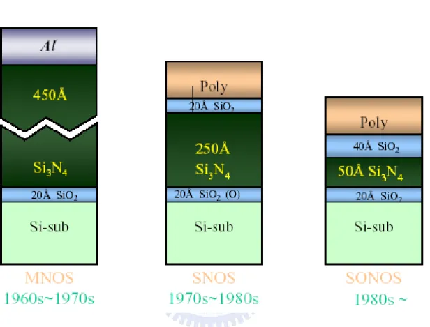
The first nitride-base devices is metal-gate nitride device MNOS (Metal/Nitride/Oxide/Silicon) which was reported in 1967 by Wegener et al [1.13].
However, it is well known that silicon nitride film contains many carrier traps which cause threshold voltage shift. Then the silicon nitride trap-based devices are extensively studied for charge storage device application in the early 70s. Fig. 1-2 illustrates the progression of device cross section, which has led to the present SONOS device structure. Initial device structures in the early 1970s were p-channel metal-nitride-oxide-silicon (MNOS) structures with aluminum gate electrodes and thick (45nm) silicon nitride charge storage layers. Write/erase voltages were typically 25-30 V. In the late 1970s and early 1980s, scaling moved to n-channel SNOS devices with write/erase voltages of 14-18 V. In the late 1980s and early 1990s, n- and p-channel SONOS devices emerged with write/erase voltages of 5-12 V. The advantages of the ONO triple dielectric structure are: (1) lower programming voltage since the blocking action of the top oxide removes any limitation on the reduction of the nitride thickness; (2) charge injection from and to the gate electrode is minimized for both gate polarities, particularly for hole injection; (3) improved memory retention since there is minimal loss of charge to the gate electrode.
The SONOS (poly-Silicon-Oxide-Nitride-Oxide-Silicon) memory devices, as shown in Fig. 1-3, have attracted a lot of attention due to its advantages over the traditional floating-gate flash device. These include reduced process complexity, high speed operation, lower voltage operation, improved cycling endurance, and elimination of drain-induced turn-on [1.14-1.16]. The main difference between floating-gate and SONOS structure is the method of charge storage. The charge storage media in the floating-gate structure is the conducting polysilicon floating-gate electrode. In the SONOS memory structure, charges are stored in the physical discrete traps of silicon nitride dielectric. A typical trap has a density of the order 1018-1019 cm-3 according to Yang et al [1.17] and stores both electrons and holes injected from the channel. The charges cannot move freely between the discrete trap locations, hence the SONOS memory device is very robust against the defects inside the tunnel oxide and has good endurance.
The SONOS memory devices still face challenge in the future for high density nonvolatile memory application, which requires low voltage (< 5V), low power consumption, long-term retention, and superior endurance. Various approaches have been proposed for improving the SONOS performance and reliability. Chen et al.
demonstrated a Si3N4 bandgap engineering (BE) control method for better endurance and
retention. A nitride with varied relative Si/N ratio throughout the film has increased the charge-trapping efficiency significantly [1.18]. Tan et al. showed that over-erase phenomenon in SONOS memory structures can be minimized by replacing silicon nitride with HfO2 as the charge storage layer. The charge retention and endurance performance
is improved by the addition of 10% Al2O3 in HfO2 to form HfAlO, while maintaining the
over-erase resistance of HfO2 [1.19]. She et al. demonstrates that high-quality nitride is
applied as the tunnel dielectric for a SONOS-type memory device. Compared to control devices with SiO2 tunnel dielectric, faster programming speed and better retention time
are achieved with low programming voltage [1.20]. Lee et al. presents a device structure of SiO2/SiN/Al2O3 (SANOS) with TaN metal gate. It is demonstrated that the use of TaN metal gate blocks electron current through Al2O3 layer more efficiently than a conventional polysilicon gate, resulting in faster program/erase speed and significant decrease of the saturation level of the erase VT [1.21].
Chen et al. studies a polycrystalline silicon thin-film transistor (poly-Si TFT) with oxide/nitride/oxide (ONO) stack gate dielectrics and multiple nanowire channels for the applications of both nonvolatile silicon-oxide-nitride-oxide-silicon (SONOS) memory and switch transistor [1.22]. The proposed NW SONOS-TFT exhibits superior memory device characteristics with high program/erase efficiency and stable retention characteristics at high temperature. Such a SONOS-TFT is thereby highly promising for application in the future system-on-panel display applications.
New device structures are also indispensable in making flash memory more scalable. Since SONOS flash memory offers a thinner gate stack than floating gate flash memory, and a FinFET structure controls the short channel effect much better than a bulk structure. It has been demonstrated that the FinFET SONOS flash memory devices with a much smaller cell size can provide both excellent performance and reliability. Therefore, FinFET SONOS memory has potential to become the candidate for the next generation flash memory [1.23-1.24].
1.1.2 Nanocrystal Nonvolatile Memory Devices
Nanostructure nonvolatile memories are first introduced in the early 1990s. IBM
researchers first proposed flash memory with a granular floating gate made out of silicon nanocrystals [1.25]. Fig. 1-4 illustrates conventional nanocrystal nonvolatile memory (NVM) device structures. It is observed that the nanocrystals are separated from each other within the gate dielectric. The term “nanocrystal” refers to a crystalline structure with a nanoscale dimension and its electronic properties seem more similar to an atom or molecule rather than the bulk crystal. For a nanocrystal NVM device, the charge storage media is in the form of mutually isolated nanocrystals instead of the continuous polysilicon layer. The limited size and capacitance of nanocrystals limit the numbers of stored electron, collectively the stored charges screen the gate charge and control the channel conductivity of the memory transistor.
Nanocrystal-based NVM devices have recently received much attention due to their potential to overcome the limitations of conventional polysilicon-based flash memory. Using nanocrystals as charge storage media offers several advantages, the main one being the potential to use thinner tunnel oxide without sacrificing non-volatility. This is a quite attractive proposition since reducing the tunnel oxide thickness is a key to lowering operating voltages and/or increasing operating speeds. This claim of improved scalability results from the local charge storage in discrete nodes, which makes the storage more fault-tolerant and immune to the leakage caused by localized oxide defects. Further, the lateral charge migration effect between nanocrystals can be suppressed by the strongly isolation of surrounded dielectric. There are other important advantages though. First, nanocrystal memories use a more simplified fabrication process as compared to conventional stacked-gate FG NVM’s by avoiding the fabrication complications and costs of a dual-poly process. Second, due to the absence of drain to FG coupling, nanocrystal memories suffer less from drain-induced-barrier-lowering (DIBL) and therefore have intrinsically better punch-through characteristics. One way to exploit this advantage is to use a higher drain bias during the read operation, thus improving memory access time [1.26]. Alternatively, it allows the use of shorter channel lengths and therefore smaller cell area. Finally, nanocrystal memories are characterized by excellent immunity to stress induced leakage current (SILC) and oxide defects due to the distributed nature of the charge storage in the nanocrystal layer.
Research in this regime has focused on the development of fabrication processes and
nanocrystal materials, and on the integration of nanocrystal-based storage layers in actual memory devices.
The fabrication of a nonvolatile memory cell requires a perfect control of four main parameters: (1) the tunnel oxide thickness, (2) the nanocrystal density, (3) the nanocrystal size, and (4) the control oxide thickness. An important consideration is the average size and aerial density of the nanocrystals. Larger-size nanocrystal array provides higher program/erase efficient due to small quantum confinement and coulomb blockade effects, and hence larger tunneling probability. However, it is desirable to reduce the nanocrystal size for better reliability (stress induced leakage during retention). So there is a trade-off between programming speed and reliability in selecting the nanocrystal size. A typical target is a density of at least 1012 cm-2, and requires nanocrystal size of 5 nm and below. Moreover, good process control is needed with regards to such nanocrystal features as: planar nanocrystal layer; inter-crystal interaction (lateral isolation); and crystal doping (type and level). Finally, it is preferred that that the fabrication process is simple and that it uses standard semiconductor equipment.
After the first proposal of a memory transistor using silicon nanocrystals as floating gates. In order to improve the data retention in NVM, double layer Si nanocrystals memory has been investigated [1.27]. It seems interesting to use Ge nanocrystals rather than Si nanocrystals because of its smaller band gap. Indeed King and Hu have recently demonstrated the superior memory properties of Ge based nanocrystal memories over those based on Si [1.28]. Recently, germanium/silicon (Ge/Si) nanocrystals have been reported to possess superior charge retention capability than Ge or Si nanocrystals.This is due to the fact that Ge has a smaller band gap than Si and thus by introducing a Si interface around the Ge nanocrystal, it would create an additional barrier height at the Ge/Si interface which makes it harder for electrons to leak out of the nanocrystal [1.29,1.30]. However, semiconductor nanocrystal memory may not be the ultimate solution to nonvolatile memory scaling, although it still attracts a lot of attention now.
In optimizing nanocrystal NVM devices, the ideal goal is to achieve the fast write/erase of DRAM and the long retention time of Flash memories simultaneously. For this purpose we need to create an asymmetry in charge transport through the gate dielectric to maximize the IG, Write/Erase/ IG, Retention ratio. One approach for achieving this
goal is to engineer the depth of the potential well at the storage nodes, thus creating a small barrier for writing and a large barrier for retention between the substrate and the storage nodes. This can be achieved if the storage nodes are made of metal nanocrystals by engineering the metal work function. The major advantages of metal nanocrystals over semiconductor nanocrystals include higher density of states around the Fermi level, scalability for the nanocrystal size, a wide range of available work functions, and smaller energy perturbation due to carrier confinement [1.31]. In addition, an electrostatic modeling from both analytical formulation and numerical simulation is demonstrated that the metal nanocrystals will significantly enhance the electric field between the nanocrystal and the sensing channel set up by the control gate bias, and hence can achieve much higher efficiency in low-voltage P/E [1.32].
Toward better NVM device performance and reliability, numerous attempts have been made using metal nanocrystals. Liu et al. reported the growth of Au, Pt, and Ag nanocrystals on SiO2 using an e-beam deposition method [1.31]. Lee et al. proposed a
NVM structureusing the Ni nanocrystals and high-k dielectrics [1.33]. Chen et al. present the stacked Ni silicide nanocrystal memory was fabricated by sputtering a comix target followed by a low temperature RTO process [1.34]. W nanocrystals on atomic-layer-deposited HfAlO/Al2O3 tunnel oxide were presented for application in a
memory device [1.35]. Using W nanocrystal double layers embedded in HfAlO to enhancement of memory window was demonstrated from the short channel devices down to 100nm [1.36]. Tang et al demonstrate that a chaperonin protein lattice can be used as a template to assemble PbSe and Co nanocrystal arrays for Flash memory fabrication. This provides a new approach to achieve a high density and good distribution uniformity nanocrystal array [1.37].
In the future, the primary drivers behind nanocrystal memories are the potential to scale the tunnel oxide thickness, resulting in lower operating voltages, and the simplicity of a single poly-silicon process. But there are still challenges await nanocrystal memories in the long road to commercialization. Nanocrystal memories have yet to deliver on most of their promises. In reality, part of the voltage gain is offset because of the poor control gate coupling. For fabrication processes, it is hard to control the uniformity of the nanocrystal size and their physical locations in the channel. It is not a surprise that
nanocrystal memories exhibit large device-to-device variation. Moreover, it has yet to be demonstrated that both the nominal and the statistical retention behavior are sufficient to meet true non-volatility requirements. Although single-dot memories have been demonstrated [1.38,1.39], but a more fundamental understanding of the scaling limits of nanocrystal memories is necessary, concentrating especially on the aspect of controlling channel conductance when relying on only a few discrete charge centers [1.40]. Finally, in order for that to happen, their claimed benefits will need to be more unambiguously substantiated, and a more appealing bundle of memory features will have to be demonstrated.
1.2 Motivation
Because the portable electronic products have been widely applied, we have known that the memory plays an important role in the market on chapter 1-1 and I won’t restate. In recent years, there are many researches on semiconductor or metal nanocrystals as memory and considerable attention has been focused on semiconductor or metal nanocrystals embedded in the silicon dioxide of a metal oxide semiconductor (MOS) device for future high speed and low power consuming memory device. The self-assembling of silicon or germanium nanocrystals embedded in SiO2 layers has been widely studied, and strong memory effect in MOS devices were reported . The major advantages of metal nanocrystals over semiconductor include (1) high density of states around the Fermi level, (2) strong coupling between the nanocrystal and the substrate (3) a wide range of available work function, and (4) smaller energy perturbation due to carrier confinement. I had chosen a kind of metal as the storage material of memory device because of those advantages. The metal material I chosen was cobalt. On the other hand, our researches were chosen cobalt or cobalt Silicide as the main materials for some reasons.
Among several kinds of nanocrystals devices, the metal and metal-silicide NCs are considered to be beneficial in its variable work function, higher density of states around the Fermi level and so on. We could know that metal silicide has been receiving attention in VLSI devices for interconnects, gate and source/drain contacts. Among the Metal
Silicide, cobalt-silicide (CoSi2) has been widely used as a contact source due to the lower resistivity value (10-18μΩ/cm) and good thermal stability . Over the past years, several studies have been made on the memory that was based on Co or CoSi2 nanocrystals. CoSi2 thin films are often employed in the semiconductor technology.
1.3 Organization of This Thesis
In chapter 1, general background of flash nonvolatile memory, SONOS nonvolatile memory and nanocrystal nonvolatile memory devices were introduced.
In chapter 2, basics of program/erase operation for memory device were discussed. In chapter 3, Cobalt-Silicide thin-film thermal treatment in O2 ambient.
In chapter 4, Cobalt-Silicide thin-film thermal treatment in N2 ambient. In chapter 5, Co-Si-O deposited by sputtered CoSi2 in oxygen ambient.
Figure 1-1 The structure of the conventional floating-gate nonvolatile
memory device. Continuous poly-Si floating gate is used as the
charge storage element.
Figure 1-2 The development of the gate stack of SONOS EEPROM
memory devices. The optimization of nitride and oxide films has been
the main focus in recent years.
Figure 1-3 The structure of the SONOS nonvolatile memory device.
The nitride layer is used as the charge trapping media.
Figure 1-4 The structure of the nanocrystal nonvolatile memory device.
The semiconductor nanocrystals or metal nanocrystals are used as the
charge storage element instead of the continuous poly-Si floating gate.
Chapter 2
Basic Principle of Nonvolatile Memory
2.1 Introduction
There is a widespread variety of Nonvolatile Memory (NVM) devices, and they all show different characteristics according to the structure of the selected cell and the complexity of the array organization. A NVM memory cell has to commute from one state to the other and that can store the information independently of external conditions. There are several methods to achieve the NVM memory characteristic, such as transistor VT shifts, charge displacements, and resistance change [2.1]. In this thesis, we focus on
one solution that a transistor with a threshold voltage that can change repetitively from a high to a low state, corresponding to the two states of the memory cell. Most operations with a shift in the threshold voltage on novel nonvolatile memories, such as nanocrystal and SONOS memories are base on the concept of Flash memory. If a datum has to be stored in a bit of the memory, there are different procedures. The threshold voltage shift of a Flash transistor can be written as [2.2][2.3]:
FC T C Q V =− Δ
where is the charge weighted with respect to its position in the gate oxide, and the capacitances between the floating gate and control gate. The threshold voltage of the memory cell can be altered by changing the amount of charge present between the gate and the channel, corresponding to the two states of the memory cell, i.e., the binary values (“1” and “0”) of the stored bit. Figure 2-1 shows the threshold voltage shift between two states in a Flash memory. To a nonvolatile memory, it can be “written” into either state “1” or “0” by either “programming” or “erasing” methods, which are decided by the definition of memory cell itself. There are many solutions to achieve “programming” or “erasing”.
Q
In this chapter, we will discuss program/erase mechanisms from the relation
between bias and energy band bending. Tunneling injection, channel hot electron injection, and band to band assisted electron/hole injection will be discussed briefly. The reliability of nonvolatile memory and physical characteristic of nanocrystal NVM will be also discussed.
2.2 Basic Program and Erase Mechanisms
2.2.1 Energy band diagram during program and erase operation
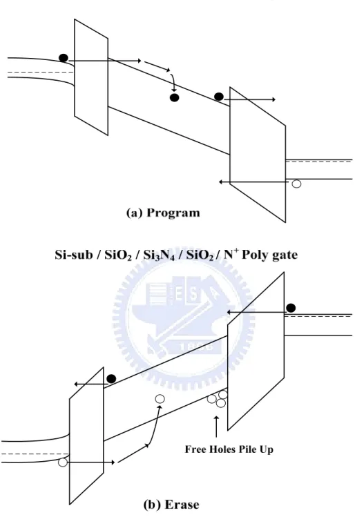
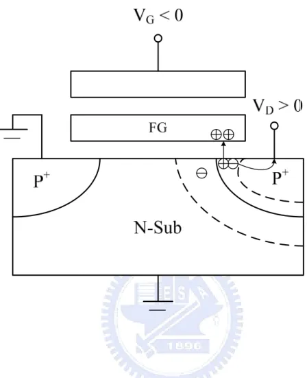
Fig. 2-2 illustrates the program/erase physical operation of a SONOS memory device. In the write operation, a positive voltage is applied on gate electrode relative to the p-type substrate, which forms an electron channel. Then the electrons tunnel through the tunnel oxide into the silicon nitride film and can be stored in deep-level traps. Some electrons which are not trapped in the nitride film will tunnel through a blocking oxide into the gate electrode. The trapped electrons provide the electrostatic screening of the channel from the control gate, and result in a threshold voltage (VT) shift. During the
erase operation under a negative voltage bias on the gate electrode, the holes tunnel from the substrate into the silicon nitride and are partially trapped in a manner similar to electrons. And some holes “pile-up” at the blocking oxide interface because of the larger barrier height (5eV). Further, trapped electrons may be de-trapped into the nitride conduction band and then tunnel back to the channel. Thus, for SONOS memory device operation both carrier types are involved in the transport process.
The write and erase processes for an n-channel semiconductor nanocrystal memory device are illustrated schematically in Fig. 2-3. During the write process, a positive gate voltage is applied to inject channel inversion-layer electrons into the nanocrystals. During the erase process, a reverse gate bias is applied to cause the electrons to tunnel back into the channel and the accumulation layer holes to tunnel into the nanocrystals from the channel.
2.2.2 Carrier Injection Mechanisms
(a) Tunneling Injection
Tunneling is a quantum mechanical process akin to throwing as ball against a wall often enough that the ball goes through the wall without damaging the wall or the ball. It also loses no energy during the tunnel event. The tunneling probability, depending on electron barrier height (φ(x) ), tunnel dielectric thickness (d), and effective mass (me)
inside the tunnel dielectric, is express as [2-4]
Basically, tunneling injection must to have available states on the other side of the barrier for the carriers to tunnel into. Tunneling through the oxide can be attributed to different carrier-injection mechanisms. Which process applies depends on the oxide thickness and the applied gate field or voltage. Direct tunneling (DT), Fowler-Nordheim tunneling (FN), modified Fowler-Nordheim tunneling (MFN) and trap assistant tunneling (TAT) are the main programming mechanisms employed in memory [2.5-2.7] as shown in Figure 2-4.
Direct Tunneling
Direct Tunneling is the flow of electrons through the full oxide thickness illustrated in Figure 2-4(a). For nanocrystal memories, the control-gate coupling ratio of nanocrystal memory devices is inherently small [2.8]. As a result, F-N tunneling cannot serve as an efficient write/erase mechanism when a relatively thick tunnel oxide is used, because the strong electric field cannot be confined in one oxide layer. The direct tunneling is employed in nanocrystal memories instead.In the direct-tunneling regime, a thin oxide with thickness less than 3 nm is used to separate the nanocrystals from the channel. During program/erase operations, electrons/holes can pass through the oxide by direct tunneling, which gives the advantages of fast write/erase and low operation voltage. In the other hand, the direct tunneling is more sensitive to the barrier width than barrier height, two to four orders of magnitude reduction in leakage current can still be achieved if large work function metals, such as Au or Pt [2.9].
Fowler–Nordheim Tunneling
The Fowler–Nordheim (FN) tunneling is the flow of electrons through a triangular
potential barrier illustrated in Figure 2-4(b). FN tunneling mechanism occurs when applying a strong electric field (in the range of 8–10 MV/cm) across a thin oxide. In these conditions, the energy band diagram of the oxide region is very steep. Therefore, there is a high probability of electrons’ passing through the energy barrier itself. Using a free-electron gas model for the metal and the Wentzel–Kramers–Brillouin (WKB) approximation for the tunneling probability [2.10], one obtains the following expression for current density [2.11]:
⎥ ⎥ ⎦ ⎤ ⎢ ⎢ ⎣ ⎡− Φ Φ = ∗ qF m h F q J OX B B 3h ) 2 ( 4 exp 16 2 3 2 1 2 2 2 3 π
Where ФB is the barrier height, is the effective mass of the electron in the forbidden
gap of the dielectric, h is the Planck’s constant, q is the electronic charge, and F is the electrical field through the oxide. The exponential dependence of tunnel current on the oxide-electric field causes some critical problems of process control because, for example, a very small variation of oxide thickness among the cells in a memory array produces a great difference in programming or erasing currents, thus spreading the threshold voltage distribution in both logical states.
∗
OX
m
Modified Fowler–Nordheim Tunneling
Modified Fowler–Nordheim tunneling (MFN) is similar to the traditional FN tunneling mechanism, yet the carriers enter the nitride at a distance further from the tunnel oxide-nitride interface. MFN mechanism is frequently observed in SONOS memories. The SONOS memory is designed for low-voltage operation (< 10V, depending on the Equivalent oxide thickness), a relatively weak electrical field couldn’t inject charges by DT or FN mechanism.
Trap Assistant Tunneling
The charge storage mediums with many traps may cause another tunneling mechanism. For example, the charges tunnel through a thin oxide and arrive to the traps of nitride layer at very low electrical field in SONOS systems. During trap assisted
injection the traps are emptied with a smaller time constant then they are filled. The charge carriers are thus injected at the same distance into the nitride as for MFN injection. Because of the sufficient injection current, trap assistant tunneling may influence in retention [2.12].
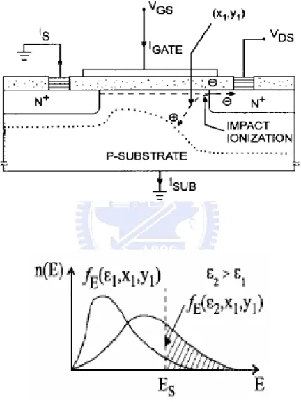
(b) Channel Hot Electron Injection (CHEI)
The physical mechanism of HEI is relatively simple to understand qualitatively. An electron traveling from the source to the drain gains energy from the lateral electric field and loses energy to the lattice vibrations (acoustic and optical phonons). At low fields, this is a dynamic equilibrium condition, which holds until the field strength reaches approximately 100 kV/cm [2.13]. For fields exceeding this value, electrons are no longer in equilibrium with the lattice, and their energy relative to the conduction band edge begins to increase. Electrons are “heated” by the high lateral electric field, and a small fraction of them have enough energy to surmount the barrier between oxide and silicon conduction band edges (channel hot electron, CHE). Figure 2-5 shows schematic representation of CHEI MOSFET and the energy-distribution function with different fields. In the other hand, the effective mass of hole is heavier than one of electron. It is too hard to obtain enough energy to surmount oxide barrier. Therefore, hot-hole injection rarely is employed in nonvolatile memory operation.
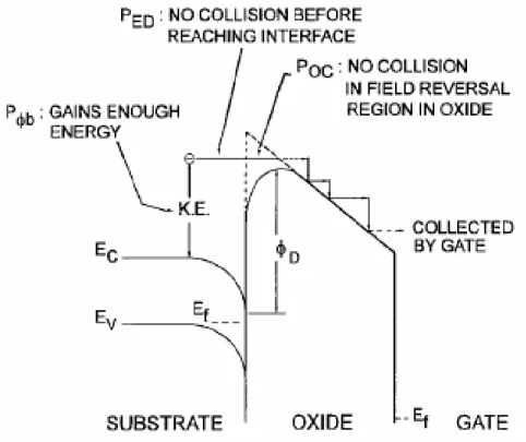
Nevertheless, a description of the injection conditions can be accomplished with two different approaches. The HEI current is often explained and simulated following the “lucky electron” model [2.14]. This model is based on the probability of an electron’s being lucky enough to travel ballistically in the field ε for a distance several times the mean free path without scattering, eventually acquiring enough energy to cross the potential barrier if a collision pushes it toward the Si/SiO2 interface. Consequently, the
probability of injection is the lumped probability of the following events [2.15], which are depicted in Figure 2-6
1) The carrier has to be “lucky” enough to acquire enough energy from the lateral electric field to overcome the oxide barrier and to retain its energy after the collision that redirects the electron toward the interface (PΦb).
2) The carrier follows a collision-free path from the redirection point to the interface
(PED).
3) The carrier can surmount the repulsive oxide field at the injection point, due to the Schottky barrier lowering effect, without suffering an energy-robbing collision in the oxide (POC).
(c) Band to Band Tunneling (BTBT)
Band to band tunneling application to nonvolatile memory was first proposed in 1989. I. C. Chen and et al. demonstrated a high injection efficiency (~1%) method to programming EPROM devices [2.16].
Band to Band Hot Electron Tunneling Injection
The injection is applied for n-type substrate nonvolatile memory device. Figure 2-7 shows the energy-band diagram and device operation during the band to band tunneling induced hot electron (BBHE) injection. When band-bending is higher than the energy gap of the semiconductor, the tunneling electron from the valence band to the conduction band becomes significant. The electrons are accelerated by a lateral electric field toward the channel region and some of the electrons with sufficient energy can surmount the potential barrier of SiO2 like hot electron injection [2.16-2.18].
Band to Band Hot Hole Tunneling Injection
In p-type substrate, when a negative gate voltage and a positive drain voltage are applied to the cell, electron-hole pairs are generated by BTBT in the drain region, as shown in Figure 2-8. The holes are accelerated by a lateral electric field toward the channel region and some of them obtain high energy. The hot holes inject into charge trapping layer through the tunnel oxide and recombine the stored electrons. This injection is used for a new erase operation for nonvolatile memory device [2.19].
2.3 Basic Reliability of Nonvolatile Memory
For a nonvolatile memory, the important to concern is distinguishing the state in cell. However, in many times operation and charges storage for a long term, the state is not obvious with charges loss. Endurance and retention experiments are performed to
investigate Flash-cell reliability. In general, NVMs are required to withstand up to 10-100K program/erase cycles (endurance) with 10-year memory retention at temperatures as high as 85 °C.
2.3.1 Retention
Retention describes the ability to the NVM to store and recover information after a number of program cycles at a specified temperature. In any nonvolatile memory technology, it is essential to retain data for over ten years. This means the loss of charge stored in the storage medium must be as minimal as possible. For example, in modern Flash cells, FG capacitance is approximately 1 fF. A loss of only 1 fC can cause a 1V threshold voltage shift. If we consider the constraints on data retention in ten years, this means that a loss of less than five electrons per day can be tolerated [2.20]. Possible causes of charge loss are: 1) by tunneling or thermionic emission mechanisms; 2) defects in the tunnel oxide; and 3) detrapping of charge from insulating layers surrounding the storage medium; 4) mobile ion contamination. Further, the retention capability of Flash memories has to be checked by using accelerated tests that usually adopt screening electric fields and hostile environments at high temperature.
2.3.2 Endurance
The term “endurance” refers to the ability of the nonvolatile memory to withstand repeated program cycles and still meet the specifications in the data sheet. In a conventional Flash memory the maximum number of erase/program cycles that the device must sustain is 105.
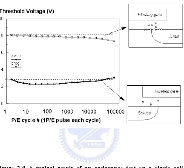
A typical result of an endurance test on a single cell is shown in Figure 2-9. As the experiment was performed applying constant pulses, the variations of program and erase threshold voltage levels are described as “program/erase threshold voltage window closure” and give a measure of the tunnel oxide aging. In particular, the reduction of the programmed threshold with cycling is due to trap generation in the oxide and to interface state generation at the drain side of the channel, which are mechanisms specific to hot-electron degradation. The initial lowering of VT the erase is due to a pile-up of
positive charge which enhances tunneling efficiency. While the long-term increase of VT
the erase is due to a generation of negative traps.
Actually, endurance problems are mostly given by single-cell failures, which present themselves like a retention problem after program/erase cycles. In fact, a high field stress on thin oxide is known to increase the current density at low electric field. The excess current component, which causes a significant deviation from the current–voltage curves from the theoretical FN characteristics at low field, is known as stress-induced leakage current (SILC). SILC is clearly attributed to stress-induced oxide defects and, as far as a conduction mechanism, it is attributed to a trap assisted tunneling, as shown in Figure 2-10. The main parameters controlling SILC are the stress field, the amount of charge injected during the stress, and the oxide thickness. For fixed stress conditions, the leakage current increases strongly with decreasing oxide thickness [2.21-2.23]
2.4 Basic Physical Characteristic of Nanocrystal NVM
2.4.1 Quantum Confinement Effect
The quantum dot, is quasi-zero-dimensional nanoscaled material, and is composed by small amount atoms. The quantum confinement energy dependence on nanocrystal size has been studied both experimentally and theoretically with the tight-binding model [2.24]. The quantum confinement effect becomes significant when the nanocrystal size shrinks to the nanometer range, which causes the conduction band in the nanocrystal to shift to higher energy compared with bulk material [2.25]. For example, a 3nm Ge nanocrystal can have a conduction band shift of 0.5eV as compared with bulk Ge, which is significant enough to affect the electrical performance of the nanocrystal memory cell.
2.4.2 Coulomb Blockade Effect
When one electron is stored, the nanocrystal potential energy is raised by the electrostatic charging energy e2
/2C, where C is the nanocrystal capacitance, which depends mainly on the nanocrystal size, though it also depends on tunnel oxide thickness and control oxide thickness. The capacitance is self-consistently calculated using an electrodynamics method [2.26]. The electron charge will raise the nanocrystal potential energy and reduce the electric field across the tunnel oxide, resulting in reduction of the tunneling current density during the write process. It is more dominant at low
programming voltages (< 3V). In a flash memory array, device cells often encounter disturbances with low gate voltage soft-programming. The Coulomb blockade effect can effectively inhibit the electron tunneling at low gate voltage and improve the flash memory array immunity to disturbance. However, the Coulomb blockade effect should be reduced by employing large nanocrystal if large tunneling current and fast programming speed were desired. The Coulomb blockade effect has a detrimental effect on the retention time, since the electrons in the nanocrystal have large tendency to tunnel back into the channel if the nanocrystal potential energy is high in retention mode. In the energy band diagram, the Coulomb blockade charging energy only raises the electrostatic potential of the nanocrystal; the quantum confinement energy shifts the nanocrystal conduction band edge upward so that the conduction band offset between the nanocrystal and the surrounding oxide is reduced.
Figure 2-1 I–V curves of the floating-gate device when there is no charge
stored in the floating-gate (curve A) and when a negative charge Q is
stored in the floating-gate (curve B).
Figure 2-2 Energy band diagrams of the SONOS memory device under
(a) program (b) erase operation.● electrons, ○ holes.
Figure 2-3 (a) Schematic cross-section of nanocrystal memory device
structure; (b) illustration of write process: inversion-layer electrons
tunnel into the nanocrystal; (c) illustration of erase process:
accumulation layer holes tunnel into the nanocrystal, electron in
nanocrystal can tunnel back to the channel.
(a) (b)
DT occur when OT OT OT X E X 2 1 1 φ φ φ > > − FN occur when OT OT X E > φ1(c) (d)
MFN occur when TAT occur when
N N OX OT OT OT X X E X ⎟ ⎠ ⎞ ⎜ ⎝ ⎛ + − > > − ε ε φ φ φ φ1 2 1 2
N N OX OT OT OT X X E X ⎟ ⎠ ⎞ ⎜ ⎝ ⎛ + > > ε ε φ φ3 3 t φ φ φ φ3 = 1− 2−
Figure 2-4 Fourth approaches to programming methods (a) Direct
tunneling (DT) (b) Fowler-Nordheim (FN) tunneling (c) Modified
Fowler-Nordheim (MFN) tunneling (d) Trap assistant tunneling (TAT).
Figure 2-5 Schematics of channel hot electron injection (CHEI). The
energy distribution function at point (X
1,Y
1) is also shown.
Figure 2-6 A schematic of energy band diagram describing the process
involved in electron injection.
Figure 2-7 Energy-band diagram for the proposed band to band induce
hot electron injection mechanism and schematic illustration cross of the
Flash memory with p-channel cell. Due to the positive bias to the control
gate, holes are not injected into the tunnel oxide.
Figure 2-8 Band to band induce hot hole injection mechanism and
schematic illustration cross of the Flash memory with p-channel cell.
Figure 2-9 A typical result of an endurance test on a single cell.
Threshold voltage window closure as a function of program / erase
cycles.
Figure 2-10 Anomalous SILC modeling. The leakage is caused by a
cluster of positive charge generated in the oxide during erase. The
multitrap assisted tunneling is used to model SILC: trap parameters
are energy and position.
Chapter 3
Formation of CoSi
2NCs or Co NCs Nonvolatile Memory by
thermal treatment in oxygen ambient
3.1 Thermal treatment in oxygen ambient
3.1.1
Motivation
The conventional nonvolatile memory (flash memory) suffers some limitations for continued scaling of the device structure. Therefore, the nanocrystal nonvolatile memory devices have been investigated to overcome the limit of the conventional floating gate memory in recently years. The main advantage for using nanocrystals serving as charge trapping centers is the potential to use thinner tunnel oxide without sacrificing nonvolatility. In addition, the operation speed can be increased and/or the operation voltage can be increased as the reduction of the tunnel oxide thickness. Furthermore, metal nanocrystals memories were widely investigated for more advantages than the semiconductor counterparts in terms of the higher density of states, stronger coupling with the conduction channel, better size scalability, and a wide range of available work functions to optimize device characteristics.
Among several kinds of NCs devices, the metal and metal silicide NCs are considered to be beneficial in its variable work function, higher density of states around the Fermi level. In addition, the dielectric layer that NCs embedded in also can contribute the charge storage sites by defects or traps created in the interfaces between different materials.
3.1.2
Experiment Procedures
Figure 3-1 showed a schematic diagram of fabricating procedure labeled as structure 1. First, single-crystal 6 inch (100) oriented p-type silicon wafers were
chemically cleaned by standard RCA cleaning. The wafers were followed by a thermal oxidative process to form 5-nm-thick dry SiO2layer as a tunnel oxide in an atmospheric
pressure chemical vapor deposition (APCVD) furnace. Then, after the growth of tunnel oxide, a 6-nm-thick cobalt silicide (CoSi2) thin film was deposited onto the tunnel oxide
by sputtering system at room temperature. The deposition of cobalt silicide film in structure 1 sputtered only with Argon plasma 24sccm and a DC power of 30W for CoSi2.
Then, the thermal treatment were at Rapid Thermal Annealling (RTA) for 700℃ in O2
and each degree for 60 seconds. Afterward, a 50 nm SiO2 were deposited by PECVD
system to form a thicker control oxide layer. Finally, the Al gate electrode was patterned and sintered to form a metal-oxide-silicon (MOS) structure. The MOS structure with CoSi2 or Co nanocrystals embedded between tunnel oxide and control oxide were
fabricated. This MOS capacitance structure has prepared for material and electrical analyses.
Electrical characteristics, including the capacitance-voltage (C-V), retention, and endurance characteristics, were also performed. The C-V characteristics were measured by Keithley 4200 and HP4284 Precision LCR Meter with high frequency 100 kHz. In addition, Transmission electron microscope (TEM) and X-ray photoelectron spectroscopy (XPS) were adopted for the micro-structure analysis and chemical material analysis.
3.1.3
Results and Discussion
Fig. 3-2 shows the capacitance-voltage (C-V) hysteresis of the structure 1. In this condition, shown in Fig. 3-2, it does not have an obvious memory window under ±10V C-V sweeping. Fig. 3-3 showed the transmission electron microscope (TEM) diagrams of the structure 1. After RTA process, the cobalt silicide thin film is still a continue film. Fig. 3-4 demonstrates the XPS spectra of Co 2P3/2 for the deposited film after RTA
treatment. It can be found that the spectrum shows one peak at ~782eV which is corresponding to Co oxide binding energy[3.1]. From xps , we can know that CoSi2 thin
film have been oxidized. Over oxidation is due to the heavy oxygen flow in the RTA process. Using capping oxide to confine oxygen flow prevent that heavy oxygen react with CoSi2 thin film.
3.2 The role of capped oxide during the formation of cobalt
nanocrystal
3.2.1
Experiment Procedures
Figure 3-5 showed a schematic diagram of fabricating procedure labeled as structure 2. First, single-crystal 6 inch (100) oriented p-type silicon wafers were chemically cleaned by standard RCA cleaning. The wafers were followed by a thermal oxidative process to form 5-nm-thick dry SiO2layer as a tunnel oxide in an atmospheric
pressure chemical vapor deposition (APCVD) furnace. Then, after the growth of tunnel oxide, a 6-nm-thick cobalt silicide (CoSi2) thin film was deposited onto the tunnel oxide
by sputtering system at room temperature. The deposition of cobalt silicide film in structure 2 sputtered only with Argon plasma 24sccm and a DC power of 30W for CoSi2.
Subsequently, a 20-nm-thick SiO2was deposited by plasma enhanced chemical vapor
deposition (PECVD) system. Then, the thermal treatment were at Rapid Thermal Annealling (RTA) for 700℃ in O2 and each degree for 60 seconds. Afterward, a 30nm
SiO2 were deposited by PECVD system to form a thicker control oxide layer. Finally, the
Al gate electrode was patterned and sintered to form a metal-oxide-silicon (MOS) structure. The MOS structure with CoSi2 or Co nanocrystals embedded between tunnel
oxide and control oxide was fabricated. This MOS capacitance structure has prepared for material and electrical analyses.
Electrical characteristics, including the capacitance-voltage (C-V), retention, and endurance characteristics, were also performed. The C-V characteristics were measured by Keithley 4200 and HP4284 Precision LCR Meter with high frequency 100 kHz. In addition, Transmission electron microscope (TEM) and X-ray photoelectron spectroscopy (XPS) were adopted for the micro-structure analysis and chemical material analysis.
3.2.2
Results and Discussion
Fig. 3-6 shows the capacitance-voltage (C-V) hysteresis of the structure 2 with pre-capped 20nm SiO2 700℃ 60 seconds by RTA. In this condition, shown in Fig. 3-6, it
has an obvious memory window of ~1.2V under ±15V C-V sweeping.
Fig. 3-7 showed the transmission electron microscope (TEM) diagrams of the structure 2 for the sample which pre-capped oxide 20nm by RTA 700℃ 60 seconds. The thickness of the as-deposited film is about 6nm. After pre-capped 20nm SiO2 700℃ 60
seconds RTA in O2, it can be found that the nanodots was nucleated on tunneling oxide
obviously. The average diameter of the nanodots is around 5nm. The density of the nanodot is about 1011 cm-2.
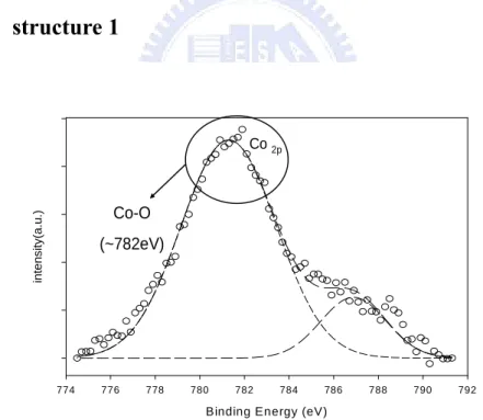
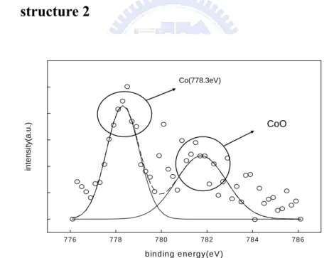
Fig. 3-8 demonstrates the XPS spectra of Co 2P3/2 for the deposited film after RTA
treatment. It can be found that the spectrum shows one peak at ~778.3eV which is corresponding to Co binding energy[3.2]. It can been confirmed that Co nanodots form after RTA annealing.
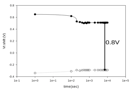
Finally, Fig. 3-9 and Fig. 3-10 showed the electrical reliability characteristics of structure 2. The endurance characteristics of pre-capped 20nm SiO2 700℃ 60 seconds
RTA in O2 showed in Fig. 3-9 which indicates the memory window can be distinguished
after 105 program/erase cycles at room temperature. As shown in Fig. 3-10, the charge retention characteristics pre-capped 20nm SiO2 700℃ 60 seconds RTA in O2 estimated
by C-t measurements at room temperature . It also indicated that the carrier charges could be kept until 104 seconds, leading to a good memory characteristic.
3.3 Gibbs free energy
In thermodynamics, the Gibbs free energy is a thermodynamic potential which measures the "useful" or process-initiating work obtainable from an isothermal, isobaric thermodynamic system. When a system changes from a well-defined initial state to a well-defined final state, the Gibbs free energy (ΔG) equals the work exchanged by the system with its surroundings, less the work of the pressure forces, during a reversible transformation of the system from the same initial state to the same final state. The change (ΔG) in Gibbs free energy is a parameter to measure a spontaneous tendency of the reaction. The ΔG is usefully defined by
ΔG = ΔH — TΔS
Where H is the enthalpy, T is temperature, and S is the entropy. If ΔG is negative, the