國立交通大學
電子物理研究所
博士論文
氮化銦鎵奈米結構之結構與光學特性
Structural and Optical Properties of InGaN Nanostructures
研究生: 蔡伩哲 撰
指導教授: 張文豪 博士
中華民國一百零一年七月
氮化銦鎵奈米結構之結構與光學特性
Structural and Optical Properties of InGaN
Nanostructures
研 究 生:蔡伩哲
Student: Wen-Che Tsai
指導教授:張文豪 博士 Advisor: Dr. Wen-Hao Chang
國 立 交 通 大 學
電子物理研究所
博 士 論 文
A Thesis Submitted to
Institute of Electrophysics College of Science National Chiao Tung University in partial Fulfillment of the Requirements
for the Degree of Doctor of Philosophy
in
Electrophysics July 2012 Hsinchu, Taiwan, Republic of China
I
氮化銦鎵奈米結構之結構與光學特性
研究生: 蔡伩哲 指導教授: 張文豪 博士
國立交通大學電子物理研究所
中文摘要
本論文旨在探討氮化銦鎵奈米結構之結構與光學特性,其主要研究內容涵蓋兩個主 題。首先,在論文的第一部份,我們針對氮化銦鎵奈米結構,進行應變釋放及成核過程 的研究。其中,我們利用拉曼光譜,針對不同大小且未覆蓋的氮化銦島狀物進行應變釋 放的研究。實驗結果指出不管透過何種方式所成長的氮化銦島狀物,其拉曼譜線的峰值 將隨著高寬比的增加而紅移。另外,我們也探討存在於氮化銦與氮化鎵介面中的初始壓 應變量,發現此應變量在島狀物剛形成時便透過塑性鬆弛的方式進行釋放,且其釋放程 度高達 96 % 以上。而殘餘約3.5 10 3的應變量將隨著島狀物的成長再以彈性鬆弛的 方式進行釋放。最後根據簡化之 2-D 模型分析及 3D 模擬結果,建立氮化銦島狀物應 變釋放的過程與大小及形貌之間的關係。此外,我們也利用有機金屬氣相磊晶系統,透 過成長溫度的改變 (550-750 °C) 成長高銦組成的氮化銦鎵奈米點,並探討其表面形 貌、合晶的組成及螢光光譜特性。我們觀察到氮化銦鎵奈米點的成核過程主要是由銦原 子所主導。其中,鎵原子溶入氮化銦的過程主要是由原子的遷移能力所決定。因此當氮 化銦鎵成長於較高的溫度時,傾向於分別形成高銦組成的島狀結構與高鎵組成的薄膜。 其中高銦組成的島狀結構其螢光訊號位於近紅外區域,而高鎵組成的薄膜則被認為是可II 見光訊號的主要來源。在討論完氮化銦島狀物在成長初期時應變釋放的過程後,我們也 研究氮化銦鎵薄膜,在不同銦組成下 (0.13<x<0.38) 其應變釋放的情況。並透過高解析 度x光繞射儀及倒置空間圖,進而探討薄膜中,應變釋放所導致銦含量分佈不均勻的特 性。根據結構上的分析,我們發現在螢光光譜上所觀察到的雙螢光譜峰與氮化銦鎵的應 變釋放情況有關。此外,我們更利用變溫及時間解析螢光光譜進一步分析此雙螢光譜 峰,並透過螢光強度隨溫度的變化及載子動態的討論,進而了解其光學特性。最後,我 們歸納出氮化銦鎵薄膜中,發光效率與侷限態效應相關的特性。 在論文的第二部分,我們利用顯微螢光光譜技術,量測奈米線寬度介於 9-27 奈米 的單根氮化銦鎵/氮化鎵奈米線。在低溫環境下,我們可觀察到氮化銦鎵中來自於侷域化 激子複合所產生的單一譜線。透過能量隨激發功率的變化,譜線隨時間飄移的情況,及 時間解析螢光光譜,我們發現極化場在氮化銦鎵/氮化鎵異質結構中並不顯著。最後經由 組成的分析及有限元素法的模擬,我們猜測銦-鎵原子在介面的擴散情況將對氮化銦鎵/ 氮化鎵異質結構的應力釋放有所影響。此外,我們也透過壓電材料,討論氮化銦鎵/氮化 鎵奈米線中,能隙隨外加應力調變的情況。實驗結果指出,螢光譜峰的能量將隨外加壓 應力而藍移。根據數值模擬的結果,發現到所外加的雙軸應力將產生一沿著奈米線之非 等向性的應變。由於在我們研究的奈米線中,並無內建壓電場及量子侷限效應,因此實 驗所觀察的螢光譜峰位移可歸納於應變所導致的能隙變化量。
III
Structural and Optical Properties of InGaN
Nanostructures
Student: Wen-Che Tsai Advisor: Wen-Hao Chang
Institute of Electrophysics National Chiao Tung University
Abstract
The dissertation is devoted to the structural and optical properties of InGaN
nanostructures. The main focus of this dissertation can be divided into two parts. First, strain
relaxation and nucleation process of InxGa1-xN nanostructures grown by MOCVD are
comprehensively studied. The Raman spectroscopy has been utilized to study the strain
relaxation in uncapped InN/GaN islands of different sizes. A redshift in the Raman peak with
the island’s aspect ratio was observed, regardless of how the InN islands were grown. Most of
the initial compressive strain at the InN-GaN interface was found to be released plastically,
with a relaxation degree up to > 96 %, during the initial stage of island formations. After that,
the residual strain of only 3.5 10 3, was further relaxed elastically via the surface islanding.
Based on a simplified 2D model analysis and full 3D simulations, we established the
relationship of the strain relaxation in InN/GaN islands with their size and shape. Besides, the
IV
by MOCVD at Tg 550-750°C have also been investigated. The nucleation of InGaN dots was found to be dominated by the surface migration of In adatoms. In particular, we found
that the incorporation of Ga into InN during the growth of InGaN dots is governed by adatom
migration capability, which tends to decompose into In-rich islands and a thin Ga-rich layer at
higher growth temperatures. In-rich islands exhibit PL emission in the NIR range, while the
formation of a thin Ga-rich layer is likely to be responsible for the observed visible emission
band. After discussing the strain relaxation of InN islands during the initial stage, the strain
relaxation in thick InxGa1-xN films with x ranging from 0.13 to 0.38 are also discussed. The In
composition inhomogeneity accompanied by strain relaxations in the InGaN films are studied
by high-resolution x-ray diffractions (XRD) and reciprocal space mapping (RSM) along an
asymmetric axis. According to the structural analysis, the observed double PL peaks are
associated with the strain relaxation in the InGaN films. Besides, further studies on double
peaks are also performed by temperature dependent and time-resolved PL. The optical
characterizations such as integrated PL intensities versus temperatures and carrier dynamics
are demonstrated clearly. Finally, the correlation between emission efficiency and localization
effect in InGaN film is also concluded.
In the second part of the dissertation, we present microphotoluminescence (μPL)
measurements on single InGaN/GaN NWs with diameters in the range of 9-27 nm. Sharp
V
can be resolved at low temperatures. Excitation dependent energy shifts, spectral diffusions,
time-resolved PL measurements of these emission lines indicate that the polarization field is
insignificant in the InGaN/GaN heterostructures. Composition analyses together with FEM
simulations suggest that In-Ga intermixing also play a role in the strain relaxations in
InGaN/GaN NW heterostructures. Besides, we also demonstrate the band-gap tuning of
InGaN/GaN NW heterostructures in the part by applying an external stress using a
piezoelectric actuator. The luminescence peak energy of InGaN/GaN NWs shows blueshift
with the applied compressive stress. According to numerical simulations, applying a biaxial
stress will induce an anisotropic strain along the NW. Due to the lack of internal electric field
and quantum confinement effect in NW heterostructures, the shift in the PL peak energy can
VI
誌謝
八年的交大生涯在隨著誌謝的撰寫下總算告一段落。回首這些年來,除了專業領域 上的成長外,在面對問題時心態上的轉變及成熟更是這些年來最重要的收穫。雖然這過 程苦樂參半,然而我卻感謝這一切的發生,感謝這歷程中陪我走過的每一個人,因為這 些都將成為我永難忘懷的回憶。 衷心感謝我的指導教授 張文豪博士,不論是在研究或是在為人處事上,老師總是 在我面前樹立了良好的楷模供我學習與成長。在研究上,老師嚴謹與執著的態度,讓我 了解到治學與做事應有的認真與嚴肅的態度。此外老師在面對問題時從容不迫的態度, 針對問題的根本尋求對策,並進而有效率的解決問題,更是讓我多所省思,獲益良多。 而我深信這些年下來的學習與成長,將對於我日後的發展有著深遠的意義與影響。另 外,我要感謝我的另一個指導教授 李明知博士。初期的博士班求學過程中,我總是不 夠成熟的處理著實驗室的事情,但老師總是給予我一次又一次的機會去學習與證明自 己,即便後來老師退休了,但我還是能體會到老師對我的關懷與照顧。師恩浩瀚無以言 謝,希望帶著從老師身上學習到的種種,在日後走出屬於自己的一片天空,不辜負老師 們的期許與教導。 感謝周武清教授這些年來的指導與鼓勵,尤其是在我遇到生活上的問題時,老師毫 不遲疑地伸出援手,給予我最需要的協助與幫忙,點點滴滴學生銘感於心。特別感謝陳 衛國教授、台大凝態中心的林麗瓊教授及其所領導的磊晶研究群,若沒有他們所提供的 半導體樣品,這篇論文是無法順利完成的。還要感謝口試委員們的指導,包括中央徐子 民教授、清大果尚志教授,謝謝委員們對我論文內的指導、建議與鼓勵,使我獲益匪淺, 在此亦表達個人內心最深的感謝。 這一段多采多姿的生活,幸賴許多學長與學弟妹們的陪伴與協助,讓我得以度過挫 折與困難。感謝古慶順博士在我剛接觸半導體光學時的引導與協助,奠定了日後許多光 學量測的概念與基礎;感謝張富欽博士、柯文政博士、李寧博士及陳京玉博士,在這一 路上給我的提攜與幫助。感謝博士班學弟妹林萱、少甫、昱安、家賢、瑋廷、衍均在這VII 幾年給予我在研究上、精神上及生活上的幫助,使得我在研究這條路上並不孤單;感謝 這八年來一起打拼的學弟妹們碧軒、啟仁、士傑、峰毅、聖允、威宇、家和、詠盛,因 為你們的貢獻與參與,我才能順利完成這篇論文。另外我還要感謝這些年來陪伴我同甘 共苦的學弟妹們,包括士凱、書鴻、士興、阿龐、志豪、小周、國榮、峰菖、健家、韋 辰、若榕,因為你們的存在,使得博士班的生活不再那麼枯燥,謝謝你們。謝謝我的學 妹詩涵,最後這一年因為你的支持與鼓勵,使得我有力量完成並拿到這得來不易的學 位。總之,該感謝的人真的很多。未被提及的師長及同伴們,請見諒,並容我在此一起 誌謝。 最需要感謝的還有我的父母及弟妹,謝謝你們全力的支持與包容,讓我能在求學路 上心無旁鶩地持續邁進。另外我還要感謝心怡,很感謝你這些年來的鼓勵與支持,不管 未來如何,真的很謝謝你在這些年對我的付出與關心。同時我也要感謝神讓我在徬徨無 助時仍能找到力量完成這條屬神的道路。 最後僅以這篇論文獻給我的家人,謝謝你們。 蔡伩哲 於工程六館 中華民國一百零一年七月三十號
VIII
CONTENTS
Chinese Abstract
... IEnglish Abstract
... IIIAcknowledgements
... VIContents
... VIIIList of Tables
... XList of Figures
... XIChapter 1 General Introduction
... 11.1 Foreword
... 11.2 Outline
... 5Chapter 2 Theoretical Background
... 72.1 Brief overview of In
xGa
1-xN growth
... 72.2 Strain effects on InN studied by Raman scattering
... 112.3 Influence of strain effect on III-nitrides
... 172.3.1 Bandgap
... 172.3.2 Piezoelectric fields
... 20Chapter 3 In
xGa
1-xN Nanostructures Grown by Metalorganic Chemical
Vapor Deposition
... 253.1 Introduction
... 253.2 In-rich In
xGa
1-xN islands
... 273.2.1 Experimental details
... 303.2.2 Size distribution of InN islands
... 313.2.3 Size dependent strain relaxation
... 363.2.4 Structural characterization of In
xGa
1-xN islands
... 423.2.5 Optical properties of In
xGa
1-xN islands
... 483.3 Ga-rich In
xGa
1-xN film
... 523.3.1 Experimental details
... 543.3.2 Discontinuous strain relaxation in InGaN film
... 553.3.3 Emission properties of strained and relaxed phase
... 60IX
Chapter 4 In
xGa
1-xN/GaN Nanowires Grown by Meleular Beam Epitaxy
... 674.1 Introduction
... 674.2 Suppressed piezoelectric electric field in single InGaN/GaN
heterostructures nanowires
... 694.2.1 Experimental details
... 714.2.2 Structural characterizations
... 724.2.3 Luminescence properties
... 744.2.4 Simulation of strain distribution
... 824.3 Bandgap tuning of InGaN/GaN nanowires
... 864.3.1 Experimental setup for applying stress
... 884.3.2 Photoluminescence spectra under stress
... 894.3.3 Simulation of strain distribution
... 92Chapter 5 Conclusions
... 97Appendixes
... 100Reference
... 104X
LIST OF TABLES
Tab. 2.1: InGaN alloys grown by MBE and MOCVD.... 9
Tab. 2.2: Raman E2 mode frequency reported for hexagonal InN. ... 13
Tab. 2.3: Elastic stiffness constants and deformation potentials for the E2 mode of InN. ... 15
Tab. 2.4: Piezoelectric constants for GaN from the literatures. ... 22
Tab. 2.5: Piezoelectric constants for InN from the literatures. ... 23
Tab. 3.1: The thickness d, the lattice constants a and c, and the In composition x of the InGaN films grown at different growth temperatures Tg. ... 58
Tab. 4.1: Simulation parameters of Young’s modulus and Poisson’s ratio. ... 93
Tab. A.1: Some important material parameters for InGaN alloy ... 100
XI
LIST OF FIGURES
Fig. 2.1: Emission wavelength versus In composition of InxGa1-xN alloys. ... 10
Fig. 2.2 : Optical phonon modes in the wurtzite structure. There are two types of the E2- and
B1-type modes that are distinguished by superscripts L and H. [Reproduced from H.
Harima, J. Phys. C 14, R967 (2002)]. ... 12
Fig. 2.3: Schematic diagram of wurtzite bandstructure. ... 18
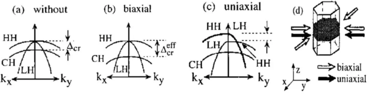
Fig. 2.4: Schematic band structure near the top of the valence bands of the WZ GaN in the kx-ky
plane ; (a) without strain, (b) with a biaxial strain, and (c) with a uniaxial strain in the c plane. The direction of each strain is shown in (d). [Reproduced from M. Suzuki et al., J. Appl. Phys. 80, 6868 (1996)]. ... 19
Fig. 2.5: The directions of the PSP and PPE in Ga-polar strained and relaxed InGaN/GaN
heterostructures. ... 21
Fig. 3.1: AFM micrographs of InN dots grown by FME and Pulsed mode with different r0: (a) 0
SCCM, (b) 500 SCCM, (c) 1000 SCCM, (d) 5000 SCCM, and ... 33
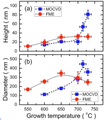
Fig. 3.2: (a) The average island height and (b) diameter of the InN islands grown by the FME and the conventional MOCVD methods as a functions of Tg . ... 34
Fig. 3.3: AFM images (10 x10 μm2) and dots size distribution of InN islands grown by (a) .. 36
Fig. 3.4: (a) Laser markers fabricated by pulsed laser. (b) AFM image of sample surface and (c) CCD image of sample surface. (b) and (c) are the same areas of sample surface. ... 37
Fig. 3.5: Four representative Raman spectra for InN islands of different sizes grown by the FME [(a) and (b)] and the PM [(c) and (d)] methods. The average island height (base diameter) for (a), (b), (c), and (d) are 47 (202), 38 (180), 22 (310) and 11 (320) nm, respectively. A spectrum taken from a 300-nm InN film is also included. ... 38
Fig. 3.6: (a) The measured Raman frequency as a function of aspect ratio. The solid ... 39
XII
Fig. 3.8: X-ray diffraction of InGaN dots grown at different temperatures. ... 45
Fig. 3.9: AES of InGaN dots grown on AlGaN buffer layer. Surface composition on dot (a), on flat region among dots (b) and on flat region after 3 min. Ar+ sputtering (c). ... 47
Fig. 3.10: Photoluminescence spectra of InGaN dots grown at different temperatures from 550 to 750°C in (a) the NIR and (b) the visible spectral ranges. ... 49
Fig. 3.11: (a) NSOM image of the 725°C grown sample mapping ... 50
Fig. 3.12: (a) X-ray diffraction and (b) PL spectra of InGaN films grown at temperatures from 675-750 oC. ... 56
Fig. 3.13: Reciprocal space mapping of InGaN films grown at (a) 675 oC (b) 700 oC (c) 725 oC (d) 750 oC. ... 57
Fig. 3.14: (a) RSM of 20 nm InGaN films grown at 675 oC. ... 60
Fig. 3.15: (a) Temperature dependent PL of InGaN film grown at 725 oC. (b)... 61
Fig. 3.16: (a) TRPL spectra of strained and relaxed phase at 12 K and ... 63
Fig. 3.17: Energy dependent TRPL of InGaN films grown at ... 64
Fig. 3.18: The measured decay time τ as a function of temperature T for (a) strained phase and (b) relaxed phase of InGaN film grown at 725 oC. The deduced radiaive τr (T) and τnr (T) lifetimes are also shown. ... 65
Fig. 4.1: Schematic illustration of InGaN/GaN NWs. The GaN NWs were grown on top of Si(111) and AlN buffer layer. The structure could be divided into nanowires (9-27 nm in diameter) and underlying columns (over 80 nm in diameter), which are grown simultaneously. At the end of the growth, 2 nm InGaN nanodisk was grown and 5 nm GaN was capped on top of it. ... 73
Fig. 4.2 : (a) A typical μPL spectrum taken from a representative single NW. (b) Power-dependent spectra for the emission lines near 2.93 eV (c) Integrated intensities and (d) peak energies of X and X* as a function of excitation power. ... 76
XIII
Fig. 4.3 : Peak energy as a function of excitation power for three different InGaN/GaN NWs
... 77
Fig. 4.4 : (a) A contour plot of the time evolution of X and X* lines constructed by consecutive spectra with an integration of 1 s for each. (b) The correlation between the integrated intensity and the peak energy of X line. (c) The correlation between the peak energies of X and X* lines. ... 79
Fig. 4.5: (a) Time-resolved PL traces for localized excitons in three different InGaN/GaN NWs. The decay traces for (b) the NW ensemble and (c) a planar sample containing a single InGaN/GaN QW. ... 81
Fig. 4.6 : (a) Calculated strain distribution of Ԑxx on the x-z plane and (b) the corresponding band profile along z at x=0 for an InGaN/GaN NW with a diameter of 18 nm. (c) Composition analysis using STEM-EDX shows that the local In composition are 2.9 %, 10 % and 3.1 % when focusing the electron beam on positions 1, 2 and 3, respectively. (d) and (e) are the same as (a,b), except that the In-Ga intermixing is taken into account. ... 83
Fig. 4.7 : Schematic illustration of the piezoelectric actuator device used to apply the biaxial stress to the InGaN/GaN NWs. ... 89
Fig. 4.8: μPL spectrum of single InGaN/GaN NW. ... 90
Fig. 4.9: (a) and (b) Color-coded PL intensity map for a NW as a function of the emission wavelength and bias voltage applied to the PMN-PT. (c) A statistics of the energy shift rate between V = -300 and 500 V from different NWs. ... 91
Fig. 4.10: Simulation of strain distribution in a NW under external ... 93
Fig. 4.11: (a) Color-coded maps of bandgap shift rate in x-y plane at ... 96
1
Chapter 1 General Introduction
1.1 Foreword
In 1994, Nakamura et al. reported the first blue light-emitting diode (LED), which was
made from a InGaN/GaN heterostructure exceeding 1cd in brightness [1]. Then blue/green
InGaN single quantum well (SQW) structures LEDs are also developed in 1995 [2]. Besides
the development in LEDs, the room temperature (RT) violet laser light emission in
InGaN/GaN/AlGaN-based heterostructures under pulsed and continuous-wave (cw)
operations were also achieved [3-5]. In 2002, the InGaN-based materials are even proposed to
fabricate high efficiency white light emitters which are predicted to play an important role in
future lighting system [6] by combining UV-emitting GaN LEDs with phosphors.
As we know, the InGaN active layers in LEDs and LDs include a large number of
threading dislocations (109-1010 cm-2), that originate from the interface between GaN and the
sapphire substrate due to the large lattice mismatch (a a16%). However, in spite of the large number of dislocations, the efficiency of the InGaN-based LEDs and LDs is much
greater than that of the conventional compound semiconductor (AlGaAs and AlGaInP)-based
LEDs and LDs. To interpret the defect-insensitive emission probability in InGaN, more
research efforts have been made and numerous models have been proposed by many research
2
LEDs to the recombination of excitons localized at potential minima originating from
InN-rich lower bandgap regions [7]. This kind of random localization of excitons was
proposed to prohibit nanradiative recombination of the excitons at threading dislocations. In
1997, the presence of In-rich InGaN [8,9] or pure InN quantum dot [10] within InGaN QW
was found to be the localization centers through transmission electron micrograph (TEM)
observations [8,9]. However, the detailed TEM studies have indicated that such dotlike
structures may be artifacts due to radiation damage during TEM observation in 2004 [11].
Furthermore, compositional or strain inhomogeneity [12] was also proposed as the origin of
exciton localization and it has often been correlated with defect-originated microstructures
[13].
In addition to defect, a c-plane LED composed of strained InGaN QWs has another
disadvantage, namely the quantum confined stark effect (QCSE) caused by the polarization
induced electrostatic fields [14]. Generally, the resulting piezoelectric field will cause the
redshifted emission energies and the lower in overlap of electrons and holes wavefunction
[15-16]. However, InGaN based LEDs still exhibit the high emission efficiency despite the
presence of above disadvantages.
Few years ago, many reports state the value of 0.65-0.9 eV for the energy gap of InN
instead of the previously accepted values 1.9 eV [17-21]. This finding has stimulated
3
extended into the near infrared (NIR) range. For instance, it provides an almost perfect match
with the complete solar spectrum, which makes InGaN a potential material for high efficiency
multijunction solar cells [22].
Besides the researches on thin film growth, the InxGa1-xN nanostructures such as
quantum dots and nanowires have also been under extensive investigations due to their
fascinating properties. For instance, the InGaN LD could improve their performance
enormously by introducing self-assembled InGaN quantum dots (QDs) into device active
layers. Higher brightness, lower threshold currents [23], and better temperature stability [24]
could result. In addition, the one dimensional (1D) nanostructures are unique because they
exhibit discrete density of states and at the same time maintain continuous transport path. A
various 1D nanostructures of GaN and InN, such as, nanorods, nanowires, nanobelts and
nanotubes, have also been synthesized successfully [25,26].
However, if we attempts to use the InxGa1-xN nanostructure as an element of the next
generation devices, more understanding of the structural and optical properties of InxGa1-xN
nanostructures are needed. Recently, with the progress of studying the InxGa1-xN
nanostructures at National Chiao Tung University, we investigate and understand the many
properties existed in InxGa1-xN nanostructures. We have employed several spectroscopy
characterization techniques to study the nanostructures, including X-ray diffraction (XRD),
4
thesis, we will present the physical characteristics of the InGaN nanostructures in many
respects, based on our recent investigations regarding their structural and optical properties.
Many phenomena involved in the thesis have been discussed and understood, but some of
them still need further studies. However, we believed that the applications of InGaN
nanostructures can be developed progressing in the next few years, if the more structural and
5
1.2 Outline
The contents of the thesis surround the structural and optical properties of InxGa1-xN
nanostructures. Before discussing the structural and optical properties, a theoretical
background is presented firstly in Chapter 2 to understand the fundamental physics happened
in the InxGa1-xN alloys. A brief review of recent advances in the growth of InxGa1-xN alloys by
MBE and MOCVD is presented in Sec. 2.1. The relationship between In composition and
emission wavelength is also demonstrated. The strain effects on InN studied by Raman
scattering are discussed in Sec. 2.2. The reported strain-free Raman frequencies of E2 mode
are reviewed briefly in the section. Besides, the estimation of residual strain through
frequency shift of E2 mode and phonon deformation potential is also demonstrated. At the end
of Chapter 2, we discuss the strain effect on III-nitrides. The bandgap and piezoelectric
polarization after strain modification is presented. Since the strain play an important role on
the electronic and optical properties, the discussions in this section can provide the further
understanding of inherent properties in III-nitrides.
The main focus of Chapter 3 is the structural and optical properties of InGaN
nanostructures grown by MOCVD. In Sec. 3.2, we present the strain state of InN islands by
Raman scattering measurements. Size dependent strain relaxation in InN islands is
comprehensively discussed. Besides, the general features of In-rich InGaN islands such as
6
Sec. 3.3, we employed the reciprocal space mapping (RSM) to study the strain and
composition distribution in Ga-rich InGaN films. Optical properties of strained and relaxed
phase existed in InGaN films are clarified in this study.
In Chapter 4, we present the unique characterizations of 1-D InGaN/GaN nanowires
grown by MBE. In Sec. 4.2, optical properties of single InGaN/GaN nanowires with thin
diameter are investigated. The suppression of piezoelectric field in a single nanowire is also
evident from the optical spectroscopy investigations. After discussing the general features of
InGaN/GaN nanowires, we demonstrated the bandgap tuning of nanowires by applying an
external stress using a piezoelectric actuator. The luminescence peak energy as a function of
the applied stress is investigated and also compared with the theoretical prediction from
COMSOL simulation package.
7
Chapter 2 Theoretical Background
2.1 Brief overview of In
xGa
1-xN growth
In the past decade, considerable efforts have been devoted to the growth of InxGa1-xN
alloys in the entire composition range using both MOCVD and MBE. However, the growth of
high quality In-rich InGaN layer remains challenging due to the low solubility of InN in GaN
which has been theoretically predicted and experimentally observed in the late 1990s [27-29].
In 1998, Karpov et al. proposed that phase separation can be suppressed during the epitaxial
growth of strained InGaN film [30]. The calculation indicated that a lower critical temperature
(750 oC) and increased solubility (35 %) can be achieved for strained InGaN alloy. The result
has been further evident by Tabata et al. in 2002 [31], where the phase separation induced by
spinodal decomposition in InGaN layers can be suppressed by biaxial strain according to
Raman measurements.
Besides, controlling the growth temperature has also been proposed to suppress the
phase separation effect. In 1999, single phase InxGa1-xN films (0.5<x<1) has been grown
successfully by MOCVD using a lower growth temperature down to 550 oC [32]. More
recently, InGaN alloys including nanowires without phase separation have been grown by
MBE or low pressure halide phase epitaxy with the entire composition range [33,34]. In this
8
MOCVD is presented. The relationship between In compositions and emission wavelengths
will also be discussed and demonstrated.
In 2002, a first set of InxGa1-xN alloys (0.36<x<1) was successfully grown by MBE [35].
From X-ray, PL, and Raman measurements, the InxGa1-xN alloys were found to exhibit only a
hexagonal structure without phase separation. Also in 2002, high quality In-rich InxGa1-xN
films (0.5<x<1) have been grown on sapphire substrate by MBE [36]. They demonstrated that
InN has narrow bandgap energy of 0.77 eV at room temperature and that the bandgap
increases with increasing Ga content. A similar finding has also been reported by Nanishi et al.
in 2003 [37], where the fundamental bandgap of InN is found to be 0.8 eV at room
temperature. Besides, InGaN films with an entire alloy composition were grown at low
temperature (550 oC) without noticeable phase separation. Based on the above results, we can
find that the single phase and entire alloy composition of InGaN alloys can be successfully
grown by MBE. This breakthrough can be attributed to the efficient atomic nitrogen species
for incorporation into the growing front, which is independent of the substrate temperature in
MBE system [38]. This advantage facilitates the growth of In-rich InGaN alloys at lower
growth temperatures without phase separation.
On the contrary, the progress in MOCVD growth of In-rich InGaN alloys is relatively
slower. Chang et al. reported that single crystalline InxGa1-xN films (0.7<x<1) can be grown
9
presence of phase separation in the InGaN alloy. In 2008, single phase InxGa1-xN alloys
(0.25<x<0.63) have been grown successfully by MOCVD [40]. They suggested that the
presence of strain and low growth temperature (610-730 oC) have promoted the suppression
of phase separation. However, further improvements in the material quality are still necessary
for the development of InGaN-based devices.
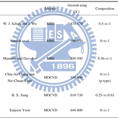
Method
Growth temp
(oC) Composition W. J. Schaff and J. Wu MBE 470-570 0.5<x<1
Nanishi et al. MBE 500-550 0<x<1
Mamutin and Davydov MBE 350-500 0.36<x<1
Chin-An Chang and Nie-Chuan Chen
MOCVD 550-900 0<x<1 (p-type) H. X. Jiang MOCVD 610-730 0.25<x<0.63 Euijoon Yoon MOCVD 640-800 0<x<1
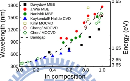
The relationship between In compositions and emission wavelengths is shown in Fig. 2.1.
It clearly indicated that InGaN alloys with emission wavelength covering from
near-ultraviolet to the near infrared range have been realized by MBE. On the contrary, only
10
the Ga-rich (x<0.3) and In-rich (x>0.8) InGaN alloys with emission wavelengths below 600
nm and beyond 1200 nm have been achieved by MOCVD growth.
0.0 0.2 0.4 0.6 0.8 1.0 300 600 900 1200 1500 1800 0.65 1.65 2.65 3.65
Ener
gy (
eV)
Davydov/ MBE J.Wu/ MBE Nanishi/ MBE Kuykendall/ Halide CVD Kim/ MOCVD Chang/ MOCVD Chen/ MOCVD BandgapW
ave
leng
th
(n
m)
In composition
11
2.2 Strain effects on InN studied by Raman Scattering
Since the strain can influence growth behaviors and optical properties of III-nitrides, it is
important to discuss and understand the strain status in the heterostructures. Raman scattering
is a nondestructive, contactless and efficient method to measure the strain exhibited in
heterostructures. In the section, we will introduce how to determine the strain state in InN
films by Raman measurements. Some experimental results of strain-free Raman frequencies
and deformation potentials will be illustrated, of which the commonly accepted values will be
pointed out.
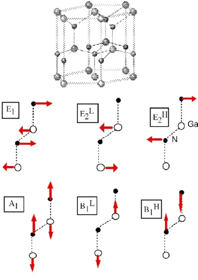
Wurtzite InN belongs to the space group 4 6v
C . Group theory predicts that there are eight sets of phonon modes at the points in the Brillouin Zone (2A1 + 2E1 + 2B1 + 2E2). The
atomic displacement scheme of these optical modes is shown in Fig. 2.2. Among them, the
2
H
E phonon mode is sensitive to the residual biaxial strain [41-43] due to the lattice displacement being parallel to the a-b-plane. In the following, the discussions will be limited
to the strain-free Raman frequencies and the deformation potentials for the 2H
12
Fig. 2.2 : Optical phonon modes in the wurtzite structure. There are two types of the E2- and B1-type modes that are distinguished by superscripts L and H.
13
Table 2.2 shows the strain-free Raman frequency for the 2H
E modes of InN reported over the past few years (1996-2002). It can be seen that the frequency is quite scattered and the reported values are in the ranges of 483-495 cm-1 for the 2H
E mode. 2 H E (cm-1) Ref. Experimental 495 44 491 45 488 46 490 47 489 18 Theoretical 483 46 492 47
Tab. 2.2: Raman E2 mode frequency reported for
14
In 2006, InN films with a thickness of about 2.3 μm were grown at different
temperatures by plasma-assisted molecular beam epitaxy (MBE) [48]. By combining the
measured Raman frequencies and the residual strains obtained from reciprocal space mapping,
the Raman frequency of 2H
E mode for strain-free InN was to be 489.8 cm-1. The deduced value is also consistent with the values reported by Pinquier et al. (2004) and Chen et al.
(2005) [49,50]. Therefore, in the thesis, we will adopt this experimental value to estimate the
residual strain in InN islands from Raman frequency shifts.
The frequency shift of E2 mode can be related to the strain by
2aabc, (2.1) where a and b are deformation potentials, while a and c are the in-plane and out-of-plane strains in InN. Using c/ a 2 / (1 ), and the reported Poisson ratio of
0.21
for InN epilayer [51], we can obtain
(2a 0.53 )b a
. (2.2)
According to the simplified equation, the residual strain can then be calculated while the
deformation potential is determined. Since the deformation potentials can be affected by the
elastic stiffness constant values, we deduce the deformation potentials aE2 and bE2 as listed
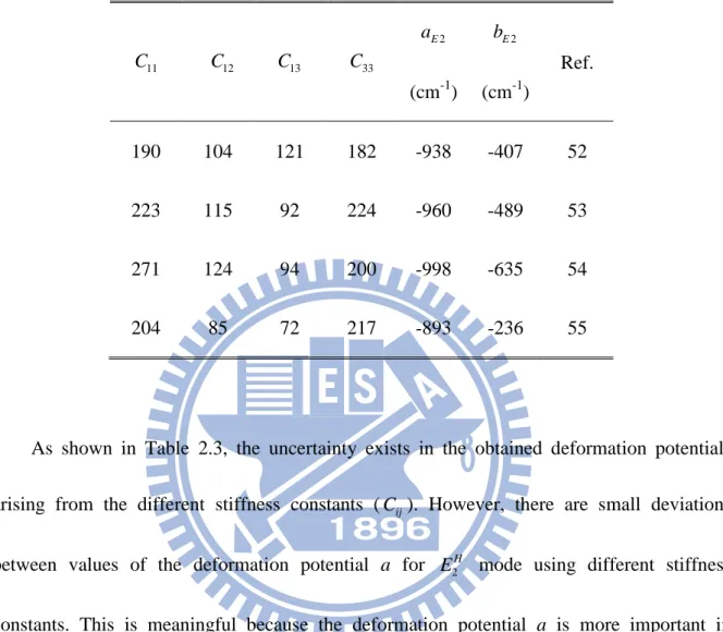
15 11 C C12 C13 C33 2 E a (cm-1) 2 E b (cm-1) Ref. 190 104 121 182 -938 -407 52 223 115 92 224 -960 -489 53 271 124 94 200 -998 -635 54 204 85 72 217 -893 -236 55
As shown in Table 2.3, the uncertainty exists in the obtained deformation potentials
arising from the different stiffness constants (Cij). However, there are small deviations between values of the deformation potential a for E2H mode using different stiffness constants. This is meaningful because the deformation potential a is more important in
determining the biaxial stresses in InN films from Raman measurements. Here, we adopt the
value reported in Ref. 30 to calculate the deformation potential in the thesis. Because the
values are smaller than AlN and close to the GaN, which is reasonable due to the weaker
bonding in InN.
Tab. 2.3: Elastic stiffness constants and deformation potentials for the E2
16
In summary, the residual strain can be estimated directly in III-nitride layers by Raman
scattering according to the shift of phonon modes, while we obtain the strain-free Raman
17
2.3 Influence of strain effect on III-nitrides
2.3.1 Bandgap
Due to the large differences in lattice constants and thermal expansion coefficients
between the substrate and the nitride layers with different alloy compositions, strain is always
present in group-III-nitride epilayers. However, this residual strain will modify the
bandstructure and electronic properties obviously. Therefore, in this section, we will brief
introduce the bandstructure of wurtzite structure firstly. Then, the influence of strain on GaN
and AlN bandgap energy will also be demonstrated.
In the wurtzite structures of GaN and AlN, the conduction band (C. B.) minimum and the
valence band (V. B.) maximum are located at the point in the Brillouin Zone (BZ), as shown schematically in Fig. 2.3. They are related to 1c, 6v and 1v states without
considering the spin-orbit interaction. Because the 6v and 1v states are separated by a
crystal field splitting, two energy gaps can be defined by
1 6 / c v A B E E E and 1c 1v c
E E E , according to the transitions 6v 1c( , )A B and 1v 1c( )C . Among them, EA B/ is the fundamental gap of GaN, whereas Ec is the transition gap of AlN due to the negative crystal field splitting.
18
Once the strain is present in the nitride layer, both the energy gap and crystal field
splitting are modified, as illustrated in Fig. 2.4.
19
To determine the bandstructure with strain, the components of strain tensor and
deformation potentials are required. Without considering the spin-orbit interaction, the three
energy bands can be described as follows:
1c( ) 1c(0) cz zz ct( xx yy) E E a a , (2.3) 6v( ) 6v(0) 1 zz 2( xx yy) 3 zz 4( xx yy) E E D D D D , (2.4) 1v( ) 1v(0) 1 zz 2( xx yy) E E D D , (2.5)
where acz, act, D1 and D2 are electronic deformation potentials, which account for the
effect of both hydrostatic and uniaxial strain contributions on the A/B energy gap. The D3
and D4 are deformation potentials that account for the strain-induced changes of the crystal-field splitting. According to the above equations, the strain induced changes in gap
energies can be simplified as follows:
Fig. 2.4: Schematic band structure near the top of the valence bands of the WZ GaN in the
kx-ky plane ; (a) without strain, (b) with a biaxial strain, and (c) with a uniaxial strain in the
c plane. The direction of each strain is shown in (d). [Reproduced from M. Suzuki et al.,
20 / ( ) / (0) ( 1 3) ( 2 4)( ) A B A B cz zz ct xx yy E E a D D a D D , (2.6) / 1 2 ( ) (0) (0) ( ) ( )( ) C A B cr cz zz ct xx yy E E a D a D . (2.7)
2.3.2 Piezoelectric fields
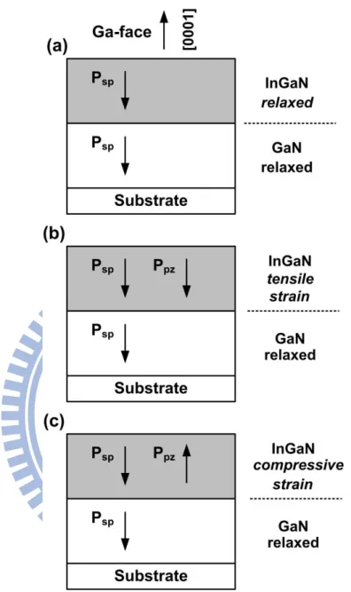
In wurtzite-structured group III-nitrides grown on c-plane sapphire substrate, strain
induced piezoelectric polarization can be expressed as
31( ) 33
pz
xx yy zz
P e e
, (2.8)
where e31 and e33 are piezoelectric constants, xx and yy are the in-plane strain, and
zz
is the out-of-plane strain. For biaxial strain, the relation between the in-plane and out-of-plane strain can be expressed as
13 33 2 zz xx C C , (2.9)
where C and 13 C are elastic constants. Accordingly, the amount of the piezoelectric 13
polarization can be determined as
13 31 33 33 2 ( ) pz xx C P e e C . (2.10) Because 13 31 33 33 (e e C ) 0 C
for InxGa1-xN over the whole range of compositions, Ppz is
always negative for layers under biaxial tensile strain and positive under compressive strain.
Consequently, the alignment of the spontaneous and piezoelectric polarization will be parallel
21
For calculating piezoelectric field in InxGa1-xN, the piezoelectric constants (e31and e33)
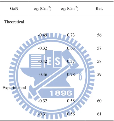
must be known and the values were usually linearly interpolated between InN and GaN. Table
2.4 and 2.5 show some reported values of e31 and e33 for GaN and InN. For GaN, the
constants are more scattered and the values from theoretical prediction is 30 % larger than
Fig. 2.5: The directions of the PSP and PPE in Ga-polar strained and relaxed
22
experimental results. On the contrary, the InN values are less scattered due to the limited data
available. GaN e33 (Cm-2) e33 (Cm-2) Ref. Theoretical -0.49 0.73 56 -0.32 0.63 57 -0.42 0.57 58 -0.46 0.78 59 Experimental -0.32 0.58 60 -0.31 0.56 61
23 InN e31 (Cm-2) e33 (Cm-2) Ref. Theoretical -0.57 0.97 56 -0.59 0.95 58 -0.48 1.06 59 Experimental -0.55 0.95 61
During 1997-2002, many piezoelectric constants have been calculated by first-principle
method [57-59]. Among them, the values for GaN reported by Bernardini et al. seem to be
much more reliable because they are in agreement with the previous calculation and some
experimental results such as laser interferometric technique [60]. However, a significant
discrepancy of about 40 % for values of GaN is also observed between the calculated and
measured results by the same method [62]. In 2003, Hangleiter et al. reported an experimental
determination of internal piezoelectric field in InGaN/GaN quantum wells with different In
compositions [61]. From the dependence of the electric filed on In composition, they derived
the piezoelectric constants e31 of GaN and InN. While the values for GaN is about 20 % below the theoretical value. The value for InN is in good agreement with theoretical data. In
24
2005, Ursula M. E. Christmas et al. used an effective-mass model to further investigate the
effect of uncertainty in the piezoelectric constants on the internal field and ground state
transition in an InGaN/GaN quantum well. They found that the piezoelectric constants
provided by Shimada et al. [57] can give the best fit to the results in the literature for
piezoelectric field and transition energy. Therefore, in the thesis, we will adopt these values to
25
Chapter 3 In
xGa
1-xN Nanostructures Grown by
Metalorganic Chemical Vapor Deposition
3.1 Introduction
In the passed several years, low-dimensional nanostructures such as nanowires and
nanodots (islands) have been widely studied due to their inherent superior properties. Among
them, InxGa1-xN nanostructures have attracted a lot of interest because of their potential use in
conventional and quantum photonics applications. Therefore, it has become an important
subject to further understand the fundamental properties of InGaN nanostructures. However, it
remains challenging to synthesize high quality InGaN nanostructures, especially for the
In-rich alloys using MOCVD growth.
In the chapter, we shall discuss our recent studies on the structural and optical properties
of InxGa1-xN nanostructures grown by MOCVD. In sec. 3.2, structural and optical
characterization of In-rich InxGa1-xN islands are discussed. Two main subjects are included in
this section. First, size dependent strain relaxation in InN islands is presented. Raman
measurements on InN/GaN islands of various sizes and shapes grown by different conditions
are discussed. The second part of this section is a study of In-rich InxGa1-xN islands. We
investigated the In-rich InxGa1-xN islands (with x0.87) grown at various temperatures by
26
measurements and near-field scanning optical microscopy (NSOM) were employed to study
the correlation among surface morphologies, alloy compositions and PL emission bands of
these In-rich InxGa1-xN islands.
In sec. 3.3, we employed the reciprocal space mapping (RSM) to study the strain and
composition distribution in Ga-rich InxGa1-xN films. Optical properties of strained and relaxed
phases are discussed. Besides, the correlation between emission efficiency and localization
effect in two phases are also presented.
27
3.2 In-rich In
xGa
1-xN island
The growth of InGaN alloys has been predicted to be challenging especially for high In
content. The difficulty arises not only from the large lattice match between InN and GaN (~11
%) but also from the high vapor pressure of N2 over InN. Consequently, phase separated or
low crystalline quality InxGa1−xN films with x > 0.2 have been grown by MBE [63] and
MOCVD [29,64-65] methods before 2000. After the recent remarkable advances in material
growth, single phase InxGa1−xN alloys (0.06 < x < 0.97) have been successfully grown by
MBE [66,67].
In addition to the progress in thin film growth, the fabrication of In-rich InxGa1-xN
islands also developed during the last few years [68-73]. Such nanostructures have attracted
much attention due to the possibilities in forming a low-dimensional system with large
confinement energy. However, the growth of high-quality In-rich InxGa1-xN island is still not
well established.
The major difficulty in In-rich InxGa1-xN island growth is large lattice mismatch between
the epilayer and the substrate material. To our knowledge, strain in the heteroepitaxial growth
can be released elastically or plastically, depending on the lattice mismatch and the surface
energy. Ng. et al. (2002) reported that the InN islands can be fromed on GaN via the
Stranski-Krastanov (S-K) mode [74]. It was proposed that InN surface islanding starts as the
28
al. further observed the strain state on InN quantum dots (QDs) on GaN/sapphire substrate by
transmission electron microscopy (TEM) [75]. They clearly indicated that the InN QD is
almost completely relaxed (97 6 %) by the formation of misfit dislocations (MDs) in the interface area, and a very low percentage of strain is relieved by surface islanding. However,
most of the published contributions are focused on the measurement of the residual strain.
Only a few reports studied the strain evolution process of In-rich InxGa1-xN islands [76].
Consequently, it is less clear whether and how the strain release via surface islanding.
In addition to the strain effect, solid phase miscibility gap in In-rich InxGa1-xN alloys is
also a controversial issue. Ho and Stringfellow [77] (1996) firstly pointed out that the
solubility of In in GaN is less than 6 % at 800 oC growth temperature. This prediction is
immediately proved by experimental observation from X-ray diffraction (XRD) in InGaN
films by Singh et al. [28] (1996). In the early 2000s, the phase separation is also evident
continuously through systematic investigations such as TEM or Raman measurements
[65,78-79]. Although this deleterious effect is hardly being avoided, it has been widely used
for forming nanoscale In-rich regions in the last decade. Because such nanostructures were
believed to act as “quantum dots” for localizing carriers and were considered to play a key
role in the high radiative efficiency of InGaN-based LEDs [10,80]. In this context,
self-assembled island growth of InGaN/GaN dots appears to be a more controllable way for
29
are still in the Ga-rich side (x0.5), with typical emission wavelength in the blue-green range. On the In-rich side (0.5 x 1), the InxGa1-xN islands with NIR emissions are still less
studied.
In this section, the initial stage of In-rich InxGa1-xN/GaN heteroepitaxial growth by using
MOCVD has been studied. The strain state, structural properties, optical properties and even
nucleation process of In-rich InxGa1-xN islands have been investigated. Firstly, Raman
measurements on InN/GaN islands of various sizes and shapes grown by MOCVD using
different growth conditions is presented. The Raman frequency is found to shift with the
island size, indicating a size dependent strain relaxation during the island formation. We show
that the residual strain after plastic relaxation at the InN–GaN interface is further relieved
elastically via surface islanding. The second part of this section is a study of In-rich InGaN
islands. We investigated the In-rich InxGa1-xN islands (with x0.87) grown at various
temperatures by MOCVD. Atomic force microscopy (AFM), x-ray diffraction (XRD),
photoluminescence (PL) measurements and near-field scanning optical microscopy (NSOM)
are employed to study the correlation among surface morphologies, alloy compositions and
30
3.2.1 Experimental details
InN islands were grown on (0001) sapphire by MOCVD using trimethylgallium (TMGa),
trimethylindium (TMIn) and ammonia (NH3) as precursors. After the growth of a 2-μm GaN
buffer layer at 1120/°C, the temperature was lowered to 625-700°C for growing InN islands.
Different gas-flow sequences and growth temperatures were used to control the InN island
size. Two series of samples were prepared. The first series was grown by the so-called
flow-rate modulation epitaxy (FME) using alternately injected TMIn [150 SCCM (SCCM
denotes centimeter per minute at standard temperature and pressure, STP)] and NH3 (18000
SCCM) gas flows. A small NH3 background flow (500 SCCM) was supplied during the TMIn
periods [85]. Three FME samples have been grown at 625, 650 and 700 ºC. Another series
was grown by the same gas-flow sequence except that a high NH3 background flow (10000
SCCM) was used. Such a growth method is similar to the so-called pulsed mode (PM), where
the NH3 flow rate was kept high, but the TMIn was pulsed injected. Three PM samples have
been grown at 700 oC using different TMIn injection time tIn 10, 15 and 20 s to control the island size.
The growth method of the uncapped InxGa1-xN islands samples is also similar with the
InN islands. The InxGa1-xN islands were grown at temperatures between 550-750 oC. The
precursor flow rates were 1, 150 and 18000 SCCM for the TMGa, TMIn and NH3,
respectively. The only difference is that a 1 SCCM TMGa flow was supplied concurrently
31
NH3 background flow rate was controlled at 10000 SCCM.
Surface morphology was investigated by atomic force microscopy (AFM). Raman
measurements were carried out at room temperature in backscattering geometry (c-axis) using
the 488-nm line of an Ar+ laser focused through a microscope objective into a spot of ~2 μm.
The scattering light was analyzed by a 1-m double monochromator with a spectral resolution
0.9 cm-1 and a peak uncertainty of about ± 0.2 cm-1. PL measurements were carried out at
T 10 K using the 325-nm line of a He-Cd laser as an excitation source. The PL signals were
analyzed by a 0.5 m monochromator and detected by either a photomultiplier tube or a cooled
extended InGaAs detector (with a cutoff wavelength at 2.05 μm) for the visible and NIR
spectral ranges, respectively. For NSOM measurements, a fiber tip was mounted on a tuning
fork of an AFM system for simultaneous measurement of the surface morphology and
emission signal using the illumination-collection mode. The tip-sample distance was kept at
~30 nm controlled by the shear-force feedback mechanism.
3.2.2 Size distribution of InN islands
It is well known that the islands size can have a great influence on optical properties such
as quantum confinement effect or strain relaxation process. Therefore, how to well control the
32
several methods have been proposed to control InN island size grown by MOCVD such as
ammonia background flows or growth temperatures.
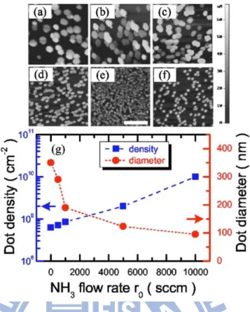
Figure 3.1 shows AFM micrographs of InN islands grown at 600 oC by FME and Pulsed
mode method with different NH3 background flow rates (r0) ranging from 0 to 10000 SCCM
[Figs. 3.1(a) – 3.1(e)] and by the conventional growth mode [Fig. 3.1(f)]. The island density
and average diameter as function of r0 are plotted in Fig. 3.1(g). As r0 was increased from 0 to
10000 SCCM, the island density increased from 8
10 2 . 6 to 10 10 0 . 1 cm−2, whereas the average base diameter decreased from 350 to 95 nm. Comparing the dot density and size to
those obtained by conventional growth mode [indicated by arrows in Fig. 3.1(g)], FME
growth under low NH3 background flows (r0 < 1000 SCCM) generally yields much larger and
less dense dots. This can be attributed to the enhanced surface migration of In adatoms in low
NH3 ambience during the deposition of In species [86,87]. As more NH3 are injected during
TMIn periods, surface migration of In adatoms is considerably hindered due to the exposure
33
In addition to ammonia background flow, growth temperature is also an important
parameter to determine the island size. Fig. 3.2 shows the statistics of island size distribution
at different growth temperatures grown by FME (r0 = 1000 SCCM) and conventional
MOCVD methods.
Fig. 3.1: AFM micrographs of InN dots grown by FME and Pulsed mode with different r0: (a) 0 SCCM, (b) 500 SCCM, (c) 1000 SCCM, (d) 5000 SCCM, and
(e) 10000 SCCM, and (f) by the conventional growth mode. (g) The density and diameter of the InN dots as function of r0.
34
The average height of FME islands increases from 11 to 30 nm as Tg was increased from
550 to 650 °C [see Fig. 3.2 (a)]. At still higher Tg, the average height remains constant at ~30
nm. In contrast, the average height of MOCVD islands increases continuously even for Tg >
700 °C, reaching 80 nm at 730 °C. Apart from the island height, their base length also
changes with the growth temperature, as evidenced in Fig. 3.2 (b). It is worth to note that the
aspect ratio (height-to-diameter ratio) of the InN islands generally increase with the increasing
Tg. For MOCVD islands, the aspect ratio is typically around ~1/10 for Tg < 700 °C and
increases to ~1/4 at Tg = 730 °C. On the other hand, the FME islands are flatter than MOCVD
islands, with an aspect ratio of ~1/16 at Tg = 550 °C and increases to ~1/8 for Tg > 650 °C.
Fig. 3.2: (a) The average island height and (b) diameter of the InN islands grown by the FME and the conventional MOCVD methods as a functions of Tg .
35
According these works, we have obtained that InN islands with controlled size and
density can be formed on GaN by using different precursor injection schemes and growth
temperatures in MOCVD. These results will help us to further study the size dependent
optical properties of InN islands.
Figures 3.3 (a) and (b) show the typical surface morphology of InN islands grown at 700
o
C by using the PM and the FME methods, respectively. The island’s shape is hexagonal with
a truncated flat top and steep faceted sidewalls. As shown in Fig. 3.3 (a), the PM-grown
islands have rather good size uniformity with flat shape and a typical aspect ratio (height/base)
less than 0.05, depending on the depositing time. However, for the FME-grown islands, the
size distribution is widespread. For the sample shown in Fig. 3.3 (b), the island height
(diameter) is from 6 to 60 nm (50 to 500 nm), with an aspect ratio ranging from 0.02-0.26.
Such a widespread size distribution allowed us to study InN islands of different sizes and
shapes on the same wafer, so that the influence of growth conditions, particularly the growth
temperature, on the strain state can be examined.
36
3.2.3 Size dependent strain relaxation
Before performing the Raman measurements to study the size dependent strain relaxation,
we have to realize the size distribution within the laser spot. Typically, the laser illuminating
spot covers a total of ~10-20 individual islands. Therefore, we have fabricated an array of
markers on the sample surface. This will help us to precisely control the position of laser spot
with an accuracy better than 0.5 μm, so that the information about the island size can be
obtained from AFM analysis. This laser marking technique is shown schematically in the Fig.
3.4. By inspecting different areas on the wafer, it is possible to locate some particular region,
where the island sizes are similar. Accordingly, Raman spectra for InN islands of different
Fig. 3.3: AFM images (10 x10 μm2) and dots size distribution of InN islands grown by (a)
37
sizes were obtained.
In Fig. 3.5, four representative Raman spectra for different island sizes grown either by
the PM or the FME are displayed, together with a spectrum obtained from a 300-nm InN thin
film. Beside the three peaks from sapphire, the InN E2-high mode near 490 cm-1 can be
observed. The Raman frequencies of InN islands are higher than that of the InN film,
indicating that islands are more compressively strained than the thin film. In particular, we
found that the Raman frequency of the InN islands redshifts with the increasing island size,
indicative of a size-dependent strain relaxation in the InN islands.
Fig. 3.4: (a) Laser markers fabricated by pulsed laser. (b) AFM image of sample surface and (c) CCD image of sample surface. (b) and (c) are the same areas of sample surface.
38
Figure 3.6 (a) shows the measured E2-high-mode frequency of InN islands as a function
of their aspect ratio ( ). A redshift in the Raman frequency with the increasing can be
seen, regardless of how the InN islands were grown. In fact, we have also analyzed the Raman
frequency as a function of island’s height or diameter [75], but the data are more scattered.
This leads us to conclude that the decreasing E2-high-mode frequency with the island aspect
ratio appears to be a general trend.
Fig. 3.5: Four representative Raman spectra for InN islands of different sizes grown by the FME [(a) and (b)] and the PM [(c) and (d)] methods. The average island height (base diameter) for (a), (b), (c), and (d) are 47 (202), 38 (180), 22 (310) and 11 (320) nm, respectively. A spectrum taken from a 300-nm InN film is also included.
39
`
The measured Raman shifts can be used to determine the in-plane strain in the InN islands of different sizes. Here we adopt the values reported in Ref. 63, where the strain-free
Raman frequency and the slope coefficient / of the InN E2-high mode was
determined to be 1
490.1 cm and 1
1660 140 cm
, respectively. As shown by the right scale of Fig. 3.6 (a), the in-plane strain of these InN islands is compressive (negative),
decreasing from 3
3.1 10
to 3
0.6 10
with the increasing from 0.026 to 0.26. It can
Fig. 3.6: (a) The measured Raman frequency as a function of aspect ratio. The solid (hollow and half-filled) symbols are data obtained from FME (PM) samples grown at different temperatures. The hollow circles with error bars are from PM grown islands with tIn = 10, 15, and 20 s. The two half-filled circles are from different
regions of the sample with tIn = 10 s.The dotted line is the exponential fitting curve.
The solid line is the average in-plane strain in disk-shaped islands calculated from 3D finite-element simulations. (b) Simulated distribution of Ԑxx in the y-z plane of an
40
be inferred that the in-plane strain would approach zero for 1, i.e., the limiting case of a column-like structure. On the other hand, as 0 (i.e., an infinite platelet structure), the measured in-plane strain would represent the initial strain 0 at the InN-GaN interface. If we
use the exponential function ( )0exp() with as a fitting parameter to
approximate the decreasing in-plane strain, the initial strain can be determined to be
0 3.5 10 3
, with the parameter 6.9. Since the theoretical lattice misfit for this
heterosystem is f (aGaN aInN) /aInN 0.0971, the deduced 0 indicated that at least
96% of the interface strain has been released at the initial stage of island formations. This
result is in good agreement with that deduced from the analysis of moiré fringes in
high-resolution transmission electron microscopy images by Lozano et al. [76,88], where the
degree of plastic relaxation was estimated to be 98 % due to the formation of MD network at
the InN-GaN interface.
The decreasing in-plane strain with the island’s aspect ratio indicates that the residual
strain (after the initial plastic relaxation) was further released elastically via surface islanding.
In order to know how the residual strain released via the island’s free borders, we consider the
ribbon model proposed by Kern and Muller [89]. Although this two-dimensional (2D) model
is limited to elongated ribbons, it simplifies the problem considerably due to the availability
of analytical expression, so that a good approximation for the relaxation of the topmost layers