Design and Implementation of JPEG Encoder IP Core
Chung-Jr Lian, Liang-Gee Chen, Hao-Chieh Chang, and Yung-Chi Chang
DSP/IC Design Lab., Department of Electrical Engineering National
Taiwan
University, Taipei 106, Taiwan, R.O.C.Te1:+886-2-2363-525 1 ext.344, Fax:+886-2-2363-8247
E-mail: { cjlian, lgchen} @video.ee.ntu.edu.tw
Abstract
-
A complete, low cost baseline JPEG encoder soft IP and its chip implementation are presented in this paper. It features user-defined, run-time re-configurable quantization tables, highly modularized and fully pipelined architecture. A prototype, synthesized with COMPASS cell library, has been implemented in TSMC 0.6-pm single-poly, triple-metal process. It can run up to 40 MHz at 3.3V. This IP can be easily integrated into various application systems, such as scanner, PC camera and color FAX, etc.I. INTRODUCTION
IP design and reuse become an hot issue in the System-on-a-Chip (SOC) era. This paper describes an IP design and implementation of an image encoding hardware architecture based on the baseline JPEG standard[ 11. JPEG is a popular international standard for continuous-tone still image coding. Such an image encoding hardware is required for more and more data-intensive image transmission applications, such as high-resolution color image scanners, digital cameras with million-pixel resolution and so on. In order to overcome the long transmission latency and huge amount storage, image compression is required for these high-resolution image-processing devices.
For applications such as PC camera, digital still camera, and scanners with compression capability embedded, a dedicated architecture with hardware-optimized configuration is a cost- effective solution. It consumes less chip area and power. This motivates the proposed IP design of JPEG Encoder. In section 11, the proposed architecture is described. The chip implementation results are shown in section 111. Finally, a conclusion is given.
11.
ARCHITECTURE
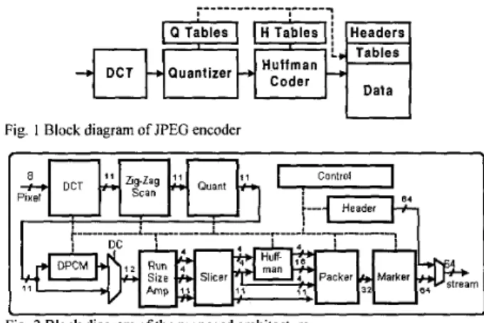
Baseline JPEG system consists of three major parts, the 2-D Discrete Cosine Transform (DCT), the Quantizer and the Huffman Coder, as shown in Fig. 1. The detailed block diagram of our proposed architecture is in Fig. 2. A cost-effective 2-D DCT module
is implemented based on the row-column decomposition architecture[2]. Zig-Zag scan module is designed through a special arrangement of memory read and write, only one 64x11 dual port memory is needed, while other design[lO] requires a 128x11 dual port memory. Also, the latency in this module is reduced by half.
Quantization is realized by utilizing table look-up method. The quantization steps stored in QT-memory address the l/Q map table to obtain the reciprocal of the quantization steps. ZZ-scan module is put in front of the Quantization module such that the quantization steps specified by user are stored in Zig-Zag scan order in the QT- memory. Quantization steps, therefore, can be sent to header module to be inserted into bitstream directly. Variable Length Code (VLC) encoder comprises differential pulse code modulation (DPCM) module, run-length coding (RLC) module, Huffman table, symbol- slicing module and bit-packing module. We have proposed an efficient and cost-effective parallel VLC encoder architecture in [3].
29
Fig. 1 Block diagram of JPEG encoder
Fig. 2 Block diagram of the proposed architecture
The proposed architecture can process the codeword and amplitude in one clock cycle. Header and X’FF’ marker insertion module is designed to produce completely JFIF-compliant[4] bitstream. No extra processor is needed to handle the bitstream syntax. The whole architecture is fully pipelined. High input data rate, one sample per cycle, and high throughput rate can be achieved so as to meet the speed requirement for various applications. Due to the smooth data flow, control circuits are designed compactly as a counter-based logic with pause function to freeze all operations. Pipeline stage insertion is very simple by changing the control parameters in compile time.
111.
IMPLEMENTATION
Various images, color and gray, with different sizes are used for functional verification. The compressed bitstreams can be decoded correctly by various image processing software. That shows the conformance of the generated bitstream. For silicon verification, this IP is synthesized with COMPASS cell library, and fabricated using TSMC 0.6vm 1P3M process. Multiplexers for testing are added to some important module I/& to view the internal nodes, which increases the observability. To exhaustively test the Huffman table, an extra counter is embedded to be the inputs of the table look-up module in the testing mode, which increases the controllability. Fig. 3. shows the chip micrograph. The design is flattened-routed with only soft constraints about cell positions to group some modules. The chip is tested using IMS ATS200 test system. It can run up to 40MHz at 3.3V. The detailed gate counts and specification of this prototype is summarized in Table 111. The measured experimental result under different voltages and frequencies is shown in Fig. 4. There is few detail and suitable comparison data available, especially commercial product. Also, due to different technology mapping and different timing constraint during synthesis, some data can not be compared directly. We try to list the reference data of [IO]
in Table I1 for comparison. It is shown that our design is a very
competent design.
JPEG encoder has become a very important IP in the market. With active pixel sensor, ADC, and JPEG encoder on one chip, compression camera SOC is a feasible solution. Scanner with compression function inside can shorten the transmission time. We have proposed a memory efficient preprocessing circuit[5] for such a scanner. As for color FAX, compound document compression[6] is a future trend. In these applications, a power, area, and speed efficient embedded 1P is the best solution for cost and fast time-to-market consideration. Pre-processing circuits such as color space transformation, and raster-to-block line buffer, etc. can be easily interfaced with this 1P through signal handshaking.
Control Others Total
IV.
CONCLUSIONS
A Soft IP design of a low cost, quantization re-configurable JPEG encoder architecture is described in this paper. Compared with other JPEG encoders[7-10], our design is more compact in chip size/cost. Moreover, fully pipelined architecture with a central controller simplifies the control of data flow. Thus, for various applications, an image compression system can be rapidly built based on the proposed JPEG core architecture.
0.5 k gates 3.9 k gates 33.5 kgutes
REFERENCES
ISO/IEC, International Standard DIS 1091 8, Digital Compression and Coding of Continuous-Tone Still Images. Avanindra Madisetti and Alan N. Willson, Jr., “A 100 MHz 2-D 8x8 DCTIIDCT Processor for HDTV Applications,” IEEE Transactions on Circuits and Systems for fide0 Technology, Vol.
5 , No.2, April 1995.
Hao-Chieh Chang, Liang-Gee Chen, Yung-Chi Chang and Sheng-Chieh Huang, “A VLSI Architecture Design of VLC Encoder for High Data Rate Video/Image Coding,” ISCASY9, June 1999.
Eric Hamilton, C-Cube Microsystems, JPEG File Interchange Format, Version 1.02, September 1, 1992
Chung-Jr Lian, Liang-Gee Chen, Hao-Chieh Chang, and Yung- Chi Chang, “Embedded JPEG Encoder IP Core and Memory Efficient Preprocessing Architecture for Scanner,” accepted by
APCCAS2000.
ITU-T Recommendation T.44 (l999), Mixed raster content (MRC).
Peter A. Ruetz, Po Tong, Daniel Luthi and Peng Hang, “ A Video-Rate JPEG Chip Set,” Journal of VLSI Signal Processing,
Martin Bolton, Richard Boulton, John Martin, Samuel Ng and Steve Turner, “A Complete Single-Chip Implementation of the JPEG Image Compression Standard,” IEEE 1991 Custom Integrated Circuits Conference.
Mario Kovac and N. Ranganathan, “JAGUAR: A Full Pipelined VLSI Architecture for JPEG Image Compression Standard,” Proceedings of the IEEE, Vol. 83, No. 2, Feb. 1995
Integrated Silicon Systems Ltd, Databook: JPEG IP Core Solutions v2.2, April 1999. URL: http://www.iss-dsp.com NO. 5, pp. 141-150, 1993.
TABLE 1
SUMMARY OF GATE COUNTS OF OUR DESIGN
Block DCT Parser CodCtrl HulEnc Packer RLEnc Quant Total
1
1.4 k g ates Marker Huffman ] 1.3 k gates Size 25 k gates 2.3 k gates 6.5 k gates 6.0 k gates 2.5 k gates 7.0 k gates 4.1 k gates 53.4 k gates Transpose Memory QT Memory ZZ Memory HT Memory 64x16, dual port 256x8, single port 128x1 I , dual port 2x512~11, single port Cell Library Technology Core Area Gate Count Transistor Count Clock Frequency Power Dissipation Package COMPASS 0.6pm TSMC 0.6pm 1 P3M CMOS 5.38 mm x 5.35 mm 33,120 (RAM excluded) 170,190 40 MHz 3 lOmW @ 40 MHz, 3.3V 144 -Pin CQFP 3.6 3 5 3.4h :::
2
3.11,
2 2 f 3.0 2.9-
2 8 3 2.6 L 2 5 2.4 2 2.3 2.2 2.1 2 .o 2 0 2 1 2 2 23 2 4 25 26 2 7 2s 2 9 30 3 1 3 2 3 3 3 4 35 36 37 38 39 4 0-
0 P a r ia
I - 0 Fdll C h c k (nS)-
7nS S t e p sFig. 4 Shmoo Plot of Measured Experiment Results