A 1600-MIPS Parallel Processor IC
for Job-Shop Scheduling
Kuan-Hung Chen, Student Member, IEEE, Tzi-Dar Chiueh, Senior Member, IEEE, Shi-Chung Chang, Member, IEEE,
and Peter B. Luh, Fellow, IEEE
Abstract—A job shop is a typical environment for manufacturing low-volume and high-variety discrete parts, where parts are of var-ious due dates, priorities, and sequences of production operations. Good scheduling of when to do what using which resource is crit-ical and challenging for the competitiveness of job shops. The La-grangian relaxation neural network (LRNN) presented by Luh et al. provides an effective solution to this problem. To further speed up the scheduling of large problems, the parallelism of the LRNN approach is exploited in this paper for hardware implementation. A parallel processor based on the single-instruction multiple-data-stream architecture and its associated instruction set are designed. The architecture is implemented in a single-poly quadruple-metal 0.35- m CMOS technology. Test results shows that the fabricated chip achieves 10 and 30 times speed-up when compared with sev-eral commercial digital signal processor chips and a 600-MHz PC, respectively.
Index Terms—Job-shop scheduling, Lagrangian relaxation neural network (LRNN), single-instruction multiple-data-stream (SIMD).
I. INTRODUCTION
S
CHEDULING is one of the critical issues for achieving op-erational efficiency in almost all manufacturing industries. Good scheduling leads to increased efficiency, utilization, and, ultimately, profitability. There have been many efforts made to-ward developing good scheduling systems for semiconductor manufacturing [1]–[4] and other industries [5]–[8], and the ef-fective resolution of scheduling problems has resulted in signif-icant savings. For example, a scheduling system reported in [5] is estimated to save over a million dollars a year for a major steel company. With the introduction of flexible machines and shop floor automation in recent years, schedules of an entire facility are now expected to be updated with a short notice to accommo-date dynamic changes such as incoming order, machine failure, Manuscript received January 15, 2002; revised May 23, 2004. Abstract pub-lished on the Internet November 10, 2004. This work was supported in part by the National Science Council, Taiwan, R.O.C., under Grant NSC-89-2212-E-002-040, and in part by the National Science Foundation, USA, under Grant DMI-9813176. An earlier version of this paper was presented at the IEEE In-ternational Symposium on Circuits and Systems, Sydney, Australia, May 6–9, 2001.K.-H. Chen is with the Department of Electrical Engineering, National Taiwan University, Taipei 10617, Taiwan, R.O.C.
T.-D. Chiueh and S.-C. Chang are with the Department of Electrical En-gineering and Graduate Institute of Electronics EnEn-gineering, National Taiwan University, Taipei 10617, Taiwan, R.O.C. (e-mail: [email protected]).
P. B. Luh is with the Department of Electrical and Computer Engi-neering, University of Connecticut, Storrs, CT 06269-2157 USA (e-mail: [email protected]).
Digital Object Identifier 10.1109/TIE.2004.841074
or other uncertainties so as to maximize an overall profit or min-imize an overall cost.
A job shop is a typical environment for manufacturing low-volume and high-variety parts [9]. In a job shop, parts with var-ious due dates and priorities are to be processed by varvar-ious types of machines. Given a set of parts to be processed and a set of machines, job-shop scheduling is to select, for each operation, a machine and the corresponding beginning time to achieve cer-tain operational objectives. Good scheduling is beneficial for machine utilization and on-time delivery of parts. How to obtain a good solution is critical to the competitiveness of any manu-facturer.
It has long been recognized, however, that the generation of optimal schedules usually requires excessive computation time regardless of the methodology used. In practical applications, solution optimality is traded off with speed, and suboptimal or heuristic-based approaches are very often used for timely de-cision making. There have been many job-shop scheduling al-gorithms [10]–[13] developed from the viewpoint of software implementation. However, there is almost no hardware-oriented approach, which can speed up the scheduling process by ex-ploiting application-specific hardware.
Recently, with the goal for hardware implementation, Luh, et
al. [14] developed the Lagrangian Relaxation Neural Network
(LRNN) algorithm for a class of job-shop scheduling problems. The LRNN algorithm combines neural network optimization capability with Lagrangian relaxation (LR) for constraint handling. Neural networks are parallel architectures that have been used to solve many optimization problems [15], [16]. The LR technique introduces a set of Lagrange multipliers to relax the system-wide coupling constraints and decompose the original optimization problem into subproblems that can be solved by neural networks mentioned above. In LRNN, a neuron-based dynamic programming (NBDP) [14] structure is developed based on the dynamic programming principles [17] to efficiently solve these subproblems. After each subproblem is solved, Lagrange multipliers are updated according to the current scheduling solution. Finally, convergence is reached and heuristic adjustment of the scheduling solution leads to a feasible near-optimal solution.
Due to the inherent parallelism in LRNN, the algorithm is suitable for parallel processing implementation. One approach is to use a cluster of computers and the other approach is to use general-purpose multiprocessing digital signal processors (DSPs). Both approaches can be regarded as coarse-grain par-allel machines [18]. Although the LRNN can run on coarse-0278-0046/$20.00 © 2005 IEEE
grain parallel machines, such configuration will degrade its ef-ficiency since the LRNN was originally motivated by massively parallel neural networks and, thus, is more amenable to fine-grain parallel implementation. We therefore present another ap-proach that adopts the concept of fine-grain parallel machines to speed up the LRNN algorithm. Instead of solving subproblems in parallel as in coarse-grain implementation, a programmable parallel processor IC is designed to exploit the parallelism in the structure for LRNN subproblem solving.
In this paper, we analyze the LRNN algorithm and develop a simplified NBDP technique for solving the subproblems in job-shop scheduling. In light of the inherent sequential nature of the dynamic programming algorithm, we design a scalable par-allel processor IC to implement the LRNN. This IC is a single-instruction multiple-data-stream (SIMD) architecture parallel processor. The processing elements (PEs) as well as the instruc-tion of this parallel processor are tailored for the LRNN algo-rithm. Test results of the fabricated chip show that the proposed chip achieves a speed-up of approximately one-tenth of the time required for the software solution for a test problem. With more processing elements, up to two orders of magnitude in speed-up can be achieved for scheduling larger problems.
The remainder of this paper is organized as follows. In Sec-tion II, details of the job-shop scheduling problem and the La-grangian relaxation methodology are formulated. In Section III, an LRNN algorithm more amenable to parallel hardware imple-mentation is introduced. Section IV describes the architecture and instruction set of the parallel processor. Circuit design of the parallel processor IC is then presented in Section V. In Sec-tion VI, physical design and measurement results of the IC are given and discussed. Finally, Section VII concludes this paper.
II. JOB-SHOPSCHEDULINGUSINGLR
Consider a job shop where there are machine types and each machine type may consist of several identical machines. There are parts to be scheduled over an overall time interval of
units (also called the time horizon). Part has its due date and weighting factor (or priority) , and has to go through operations. The processing of each operation requires a machine of a specific type for some prespecified units of time, and must satisfy the following processing time requirements:
(1) where , and represent, respectively, the beginning time, processing time, and completion time of operation of part . Also, each operation may be started only after the completion of its preceding operation, i.e.,
(2) Assume that one machine can only process at most one part at a time. It is obvious that the number of operations assigned to machine type at time should not be more than the number of machines available at that time, , i.e.,
(3)
where is a 0–1 variable and equals 1 if operation of part is being processed by a type- machine at time ; it equals 0 otherwise. Values of variables are determined once the beginning times of all operations are decided.
The scheduling goal of on-time delivery for individual parts is modeled as penalties on part delivery tardiness , where is the completion time of part . The scheduling problem then boils down to
(4) subject to constraints (1)–(3). Note that this formulation falls into the class of separable optimization problem. By exploiting the separability, the Lagrangian relaxation (LR) method uses the
Lagrange multipliers [14]
to relax machine capacity constraints (3). The relaxed problem is given by
with
(5)
subject to constraints (1) and (2). After regrouping the terms in (5) according to parts, we obtain the following independent part subproblems for a given set of Lagrange multipliers :
with (6)
subject to constraints (1) and (2) of part .
Let denote the machine type used by the th operation of part . Then by the definition of , we can rewrite (6) as
with (7)
subject to constraints (1) and (2) of part .
For a given set of Lagrange multipliers , part subprob-lems can be solved independently among the parts. After solving a part subproblem and obtaining the beginning times of its op-erations, the multipliers are updated according to
(8)
where is the step size. One iteration of the method consists of solving all part subproblems and updating the corresponding multipliers. With proper step sizes, iterative adjustment of mul-tipliers will lead to the convergence of solution. Since the solu-tions of part subproblems, when put together, may result in an infeasible schedule, i.e., machine capacity constraints might be violated in some instances, a heuristic [14] is then used to adjust the schedule to feasibility. In the heuristic, a list of immediately performable operations is created in the ascending order of their beginning times from part subproblem solutions. Operations are then scheduled on the required machine types according to this
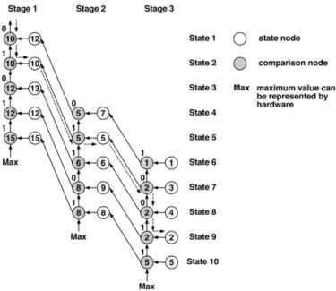
Fig. 1. Structure of the NBDP scheme.
list as machines become available. If the capacity constraint for a particular machine type is violated at time, a greedy heuristic determines which operation should begin at that time and which ones are to be delayed by one time unit. The subsequent oper-ations of those delayed ones are then delayed by one time unit if precedence constraints are violated. The process repeats until the last operation in the list.
III. LRNN ALGORITHM
Based on the above LR solution framework, Luh et al. de-veloped an LRNN algorithm for job-shop scheduling problems [14]. The novelty of their approach lies in an NBDP for solving individual part subproblems and an efficient method used to up-date Lagrange multipliers.
The main procedures in the LRNN algorithm are as follows: 1) neuron-based dynamic programming (NBDP) to compute
costs of all possible scheduling for a subproblem; 2) forward sweep to find the legitimate schedule with the
optimal cost for the above subproblem;
3) per-subproblem updating of Lagrange multipliers; 4) cyclic iteration among subproblems until convergence of
the relaxed scheduling problem;
5) heuristic adjustment of subproblem solutions to obtain a feasible schedule.
Procedures 1)–4) require intensive computation. In this section, we will analyze and modify them for parallel hardware imple-mentation.
A. NBDP
Fig. 1 shows the NBDP structure for a part having three op-erations with processing times 3, 2, and 1, respectively, and in the figure, stages correspond to operations and states corre-spond to operation beginning times. The part index is omitted for notational simplicity. The backward dynamic programming (DP) method [17] is utilized to solve the part subproblem in a stage-by-stage iterative procedure that starts from the last stage.
For state at stage , there is a state node (SN) and a comparison node (CN). First, each state is associated with a stage-wise cost given that the processing of the th operation begins at that state (time). According to (7), the stage-wise cost is the summation of all multipliers of the machine type under consideration during the processing of the operation,
i.e., , where and are the
processing time and machine type of the stage (operation). The stage-wise cost is high when it is costly to schedule the opera-tion to begin at that state. The optimal cost-to-go (OCTG) for an SN represents the minimum cost to schedule the remaining operations after completing stage (the th operation). For a state in the last (right-most) stage, the OCTG equals to the tardiness penalty of that state. The SN computes its cumulative
cost by adding its stage-wise cost and the OCTG given that the
processing of the th operation begins at that state.
The computation of OCTGs for states in the th stage is performed state-by-state by CNs in stage starting from the bottom-most state. In the procedure, output of the CN of state in stage is fed to the CN of state in the same stage. The CN of state then performs a pair-wise comparison between the cumulative cost of state obtained from the SN of state (cost associated with beginning the operation at state ) and the output from the CN of state (cost asso-ciated with beginning the operation after state ), and finds the minimum as its output (see Fig. 1). After these comparisons are sequentially performed from the bottom-most state to the top-most state, the output of the state- CN represents the
min-imum cumulative cost among states .
This value then serves as the OCTG input to state of stage as its OCTG, where is the processing time of operation .
In summary, as the DP algorithm moves backward from the last (right-most) stage to the first (left-most) stage, cumulative costs for stage are first computed based on the stage-wise costs and the OCTG of stage and then the CNs find the OCTGs for stage . Computations by both SNs and CNs are functionally repetitive from one stage to the next. The optimal subproblem cost is then the minimum of the cumulative costs in the first (left-most) stage.
B. Forward Sweep and Lagrange Multiplier Updating
In addition to obtaining the optimal subproblem cost , we need to find the beginning times of all operations. This is achieved by using a decision flag at each CN to record which of two operands is smaller in the pair-wise comparison procedure to find the OCTG. A flag of value “1” indicates that the cost is smaller if the operation begins at the particular state, while a “0” indicates that the cost is smaller if the operation does not begin at the particular state. Beginning times of all the opera-tions are thus identified from these flags by the forward sweep procedure that searches through all the necessary flags stage by stage starting from the first (left-most) stage. Within stage , the search is done state-by-state starting from the state corre-sponding to the earliest possible beginning time, which is equal to the beginning time of stage plus the processing time of the th operation. The beginning time of stage is set to
the first state with its CN flag equal to “1” in this search. An ex-ample of the forward sweep procedure is also shown in Fig. 1. Numbers in white circles represent cumulative costs, and num-bers in gray circles represent OCTGs from the preceding stage. The dashed lines show the optimal path taken during the for-ward sweep. The optimal beginning times are state 2 for stage 1, state 5 for stage 2, and state 9 for stage 3. Note that the earliest possible beginning time of the third operation (stage) is state 7, however, the third operation does not start until state 9 because of higher costs in states 7 and 8. After one subproblem is solved and its minimum cost and beginning times found, the Lagrange multipliers are adjusted by (8). Given the new beginning time and the old beginning time of each operation of this subproblem, all affected Lagrange multipliers can be updated.
C. Algorithm Analysis and Modification
The NBDP is the most computation-intensive step in the LRNN algorithm. Some of its processing steps such as the cumulative cost computation and the multiplier updating can be computed in parallel. However, the comparisons for finding the OCTG and the forward sweep procedure are inherently sequential with strong data dependency and thus cannot be parallelized. Further analysis shows that the forward sweep involves only bit comparison while the comparison in a CN re-quires subtraction of two integers. Therefore the sequential CN comparisons in NBDP, especially when the number of states is large, is a bottleneck for parallel hardware implementation of the LRNN algorithm.
To improve the speed of the LRNN method, we developed a modified search method [19], [20] that limits the search ranges that the CNs need execute comparison and thus reduces the data dependency. Numerical simulation shows that the scheme ob-tains solutions with approximately the same quality as the orig-inal NBDP scheme. In addition, finite-word-length simulations of several typical job-shop scheduling problems are also con-ducted to find the minimum word length that achieves accept-able solution quality.
IV. SIMD PROCESSORDESIGN
In the LRNN, most processing in a state is identical to that of other states except on different data. Such a feature naturally leads to an SIMD architecture for the parallel LRNN hardware realization.
A. Overall System Architecture Design
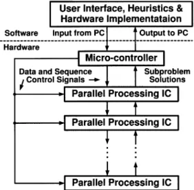
An SIMD-type parallel processor IC is developed for NBDP and multiplier updating. In this chip, the processing in a state is handled by one PE, and speed-up is achieved because of the parallelism provided by the PEs. Only a limited number of PEs can be integrated into one parallel processor IC, therefore, only problems with limited numbers of states (time horizon) can be tackled. For typical applications, several SIMD-type ICs may be cascaded to accommodate problems with long time horizons. In addition, current beginning times of all stages in all subprob-lems need be stored for computation of new beginning times. To support the cascading, beginning time storage, and problem
Fig. 2. Overall system architecture for solving the job-shop scheduling problem using the IC.
Fig. 3. Block diagram of the parallel processor IC.
setup, a microcontroller is used to control all cascaded parallel processor ICs and provide temporary data storage.
The overall architecture for solving job-shop scheduling problems using the IC is shown in Fig. 2. It consists of a personal computer, a microcontroller, and one or multiple parallel processor ICs. According to the specifications of a job-shop scheduling problem to be solved, software in the host PC applies Lagrangian relaxation to the problem and generates the adequate data and control sequences. The data and control sequences are sent to the microcontroller. The microcontroller then feeds the data from PC to the parallel processor ICs, controls their processing sequence (program), and finally re-turns the solution to the host PC. The IC is used to perform NBDP, forward sweeping, and multiplier updating. Finally, the software in the host PC performs heuristic adjustment of the LRNN solution to obtain a feasible solution. For the remainder of the paper, we will focus on the design and implementation of the parallel processor IC.
B. Parallel Processor IC Design
The block diagram of the parallel processor IC is presented in Fig. 3. Each PE is used to perform arithmetic operations such as addition, subtraction, comparison, etc., associated with the processing in a state. Within a PE, the cumulative cost of a state
is computed; pair-wise comparison of cumulative costs is made; and Lagrange multipliers associated with a state are updated.
For easy access of the Lagrange multipliers, the multipliers associated with state are stored in the corresponding PE. With this local multiplier storage scheme, the SN and CN functions and multiplier updating associated with a particular state can all be performed without incurring com-plex inter-PE data exchange. In addition, a forward sweep cir-cuit is designed specifically to perform the forward sweep, and a global memory is used to store global data such as due-date or step-size required for LRNN implementation. Finally, an in-struction decoder is used to decode inin-structions from the micro-controller into signals that control the proper functioning of all PEs and other circuitries. With this linear PE arrangement and local multiplier storage, our design provides the cascading capa-bility because data communication between two ICs is limited to that between the top-most PE in one IC and the bottom-most PE in the other IC.
How the IC may be applied to a job-shop scheduling problem is summarized as follows. Assume for simplicity of description that only one IC is required, i.e., no cascading. Instructions from the microcontroller are sequentially fed into the chip and de-coded into control signals by the instruction decoder. Control signals are sent to functional blocks on the chip through a con-trol bus and executed in the following way:
1) The OCTGs for all states of the last stage of a subproblem are calculated by all PEs and comparison results are stored in the corresponding PEs ( states).
2) The OCTGs are calculated stage by stage, from the last stage to the first, by all PEs ( stages).
3) After calculations for the first stage is completed, the forward sweep circuit finds, stage by stage, the new beginning times of all stages according to the locally stored comaprison results (decision flags). A subproblem is solved after the beginning times of all stages are found ( stages).
4) All PEs then perform multiplier updating according to the difference between the new and the old beginning times ( stages).
5) Another subproblem is then solved using the same proce-dure. Once all the subproblems are solved, an iteration is completed ( subproblems).
6) The PC determines the number of iterations to be executed based on a preset stopping criterion ( iterations). 7) Finally, a heuristic adjusment is made to resolve machine
capacity violations.
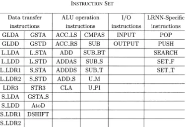
C. Instruction Set Design
To implement the LRNN algorithm over the PEs, an instruc-tion set is designed as listed in Table I. The instrucinstruc-tions are cat-egorized into four types.
1) Data transfer instructions are needed for the transferring of data between local/global memory and registers. For example, the instruction GLDA loads data from the global memory into a register.
TABLE I INSTRUCTIONSET
2) Arithmetic logic unit (ALU) operation instructions are used to perform arithmetic operations such as cost calcu-lations, cost comparisons, etc.
3) I/O instructions are for data communications between the microcontroller and the parallel processor ICs.
4) LRNN-specific instructions, e.g., the instruction PUSH pushes the result of the CN comparison into a stack so that we can pop it out later during the forward sweep. To further speed up LRNN processing, several special instructions were designed in such a way that two to three arithmetic and data transferring operations are combined into one single-cycle instruction. For example, a CN comparison for finding the OCTG at state involves a pair-wise com-parison, storing the minimum in a register, and shifting that minimum to the PE associated with state . We design an instruction (CMPAS) to execute the above three operations in one clock cycle. Instructions ADDAS and ADDDS are also multiple-operation instructions. A software program of the modified LRNN algorithm is coded using these instructions. Its execution results are compared with those of a C-language implementation. Consistency in those two sets of results verifies the completeness and correctness of the instruction set.
V. CIRCUITDESIGN
In the parallel processor IC, there are four major blocks: global memory, instruction decoder, forward sweep circuit, and PE. Among the four, global memory can be easily implemented by on-chip SRAM. Instruction decoder is a combinational logic block that can be easily designed by modern synthesis software. In this section, we will only describe the detailed design of the PE and the forward sweep circuit.
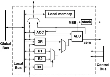
A. PE Design
Processing elements constitute the most important functional block in the IC. The circuit architecture of a PE is shown in Fig. 4. An ALU is required to perform arithmetic operations such as additions, subtractions, and others (see Table I). Regis-ters R1, R2, and R3, ACC, and DR are introduced to latch the ALU inputs, while the ALU output is either stored in ACC or routed to DR of the PE above. Within the SIMD architecture, all PEs execute the same sequence of instructions. However, it
Fig. 4. Block diagram of the processing element.
is sometimes necessary to execute different operations in some PEs. Registers R1, R2, and R3 are thus introduced to store pre-vious results for conditional execution of arithmetic operations. The local memory is required to store the Lagrange multi-pliers and the multiplier adjustment in (8) for each ma-chine type ( machine types). A local bus is used for data com-munication between the local memory and the registers such as ACC and DR. Global data communication is through the global bus and possibly the local bus of a PE. Finally, a stack is in-cluded in the PE to record the decision flags of all stages, which are used later in the forward sweep.
As an example, we describe briefly how to calculate the stage-wise cost for each state using the PE. The stage-wise cost is defined as the sum of all multipliers associated with the machine type needed during the processing time of the stage (operation). In other words, for state of stage in the th subproblem, the processing time of the stage is and the required machine type is , and the stage-wise cost is following (7). In principle, additions are needed. To do these additions in parallel without incurring too many data accesses, a parallelized procedure is devised. First, all ACC are cleared. Then since are stored in the local memory, the corre-sponding multipliers are loaded into DR in all PEs. The ALU performs ACC DR and the sum is stored into ACC. Data in all DR are shifted upward in parallel and is then propagated to state from state , which are executed using a single-cycle instruction, ADDDS. Then all ALUs perform ACC DR and the data in DR is shifted upward again. Repeating this procedure times, the ACC of the th PE will then have the stage-wise cost for the th state, i.e., , and so do the ACCs of other PEs.
The previous paragraph has shown the advantage of the local multiplier storage scheme. Now, we briefly describe how to compute OCTGs by the PEs. As mentioned in Section III-D, a modified search method was developed [19], [20] that limits the search ranges that of the CNs need execute comparison to improve the speed. Suppose that state corresponds to the be-ginning time of previous iteration and is the search range,
Fig. 5. Search process of beginning time in the forward sweep circuit. then states between and are selected for the CN comparison procedure. At first, the cumulative cost of state is stored in the ACC of the th PE and the DR of the th PE, for , and flag CMPAS EN is set to “1” for the PE corresponds to state . Note that only those PEs with a “1” value in CMPAS EN will actually execute the CMPAS instruction. Then the instruction CMPAS is fed to all PEs but only the PE corresponds to state compares two num-bers in ACC and DR, stores the minimum in ACC, stores the decision flag into a stack, shifts the minimum into DR of the th PE, and transfers the token to the th PE. All of these are executed within one clock cycle. Now the OCTG of state is stored in ACC of the corresponding PE. Repeating the CMPAS instruction times, OCTG values of states within the range are stored in the ACCs of the corre-sponding PEs.
B. Forward Sweep Circuit
Previously, we explained how the forward sweep is supposed to work. For stage of part , the search for the new begins from state downward, so that the operation precedence constraints are not violated. The first state with a decision flag of value “1” is located and recorded as the new beginning time, , of the current stage.
In the hardware implementation, the forward sweep circuit is designed to implement the forward sweep procedure stage by stage from the first stage to the last stage. A logic unit is de-signed and each state has one such logic unit, and these units are cascaded to form the basic structure of the forward sweep circuit as shown in Fig. 5. The per-stage forward sweep is imple-mented sequentially from the top-most state to the bottom-most state in the search range. The logic unit has three binary inputs:
begin flag, decision flag, and search in. The begin flag is “1”
if and only if the state corresponds to the beginning time plus the processing time of the previous stage. It indicates the earliest allowable beginning time of the current stage where the search process begins downward to locate the first state with a decision flag of “1”. The decision flag is the result of the CN comparison of the current state at the current stage. Signal search in aids the downward search and will be set during the search process as follows. It is “0” for those states above the state with a “1”
Fig. 6. “Search bypass” conditions in the forward sweep circuit.
the newly-found beginning time, and it is set to “1” in other states. In other words, search in will be “0” in those states that cannot be the new beginning time, thus eliminating them in the search for the new beginning time.
The forward sweep logic unit has two binary outputs:
search outand time flag. The search out of the logic unit in state serves as the search in of the logic unit in state . The time flag is set to “1” if and only if the state (time) is selected as the new operation beginning time, i.e., the first state that has a “1” in decision flag and is no less than the state with a “1” in begin flag.
The search procedure in the forward sweep can now be illus-trated by Fig. 5. The earliest allowable beginning time is decoded by the begin flags, with one begin flag per state. The begin flag of state 2 in the figure has value “1’ and all others have value ‘0’. The search in is initially “0” and becomes “1” after encountering the “1”-valued begin flag at state 2. After the search in becoming “1”, we search the first decision flag with “1” value. When the first “1” value decision flag at state 4 is found, we set the time flag of state 4 to be “1” and reset its search out.
The aforementioned search process is inherently sequential due to data dependency. It will therefore be very time-con-suming for large problems. To reduce the time required for the search process, we adopted the “carry bypass” concept in Manchester carry chain [21] and designed a “search bypass” scheme that will greatly reduce the search time. The forward sweep block in the chip is divided into several sections. Under some conditions the search in can bypass a whole section, greatly speeding up the search process.
Two “bypass” conditions are illustrated in Fig. 6. As shown in Fig. 6(a), if the decision flags of all states in one section are “0”, then a “1” search in can be bypassed on to the next section. If the search in input to the section is “0” and all begin flags in the section are “0”, then search in can also be bypassed as shown in Fig. 6(b). The time required for the search process can be reduced approximately to the time for searching two sections state by state plus the time to bypass the search in section by section from top to bottom of the chip.
VI. IMPLEMENTATION ANDMEASUREMENTS
Detail circuit design of the parallel processor IC was de-scribed in the gate level using a hardware description language.
Fig. 7. Die microphotograph.
Fig. 8. Maximum clock rate of the IC under different supply voltages.
TABLE II
SUMMARY OF THEPARALLELPROCESSORIC
Functional verification of the circuit design was conducted by using a five-part test problem. Layout of the parallel processor IC was generated through the standard-cell-based design flow. Functional and timing simulations of the layout were carried out. The finished layout is approximately 4.56 4.24 mm in a single-poly quadruple-metal 0.35- m CMOS technology and contains approximately 356 000 transistors. The die photo-graph of the fabricated parallel processor IC is shown in Fig. 7. There are 16 processing elements arranged in two columns. The global memory, the instruction decoder, and the forward sweep circuit are integrated into a block below the processing elements. The global bus and the control bus cross the PEs from top to bottom in the middle.
TABLE III PERFORMANCECOMPARISON
Functional correctness of the fabricated IC was verified under various clock rates and various supply voltages. The maximum clock rates under various supply voltages are shown in Fig. 8, and we can see that the parallel processor IC is functionally correct at 100-MHz operating frequency under a supply voltage of 3.3 V. With a 3.3-V supply voltage, the power dissipation of the IC is 742 mW at a speed of 100 MHz. Table II summarizes the key features of the parallel processor IC.
Two test problems are used to examine the performance of the IC. Problem A is a five-part problem with a time horizon of 16, and problem B is a 20-part problem with a time horizon of 128. Assembly codes implementing the LRNN algorithm are written by using instructions provided by our parallel processor and several commercial DSP chips, respectively. The numbers of instructions needed for the parallel processor IC and for sev-eral commercial DSP chips to solve these two test problems to similar levels of solution quality are then derived. Computation time is then calculated according to the following formula:
(9) In the above, the instruction count is the number of instructions that needs to be executed to solve a problem. Cycle per tion (CPI) is the average number of clock cycles that an instruc-tion needs. The CPI of our instrucinstruc-tion set is 1 and the cycle time is 10 ns.
Recall that the key parameters of job-shop scheduling prob-lems are as follows:
part number
average operation number per part average processing time per operation time horizon
search range
After careful examination of the program, the required instruc-tion count for solving one iterainstruc-tion of a job-shop scheduling problem is given by
(10) For example, in problem B,
, and . Substituting the above parameters into (10), we obtain the number of instructions to complete 100 iterations is approximately , which amounts to 6.54 ms at a clock rate of 100 MHz. The computation times for the DSP chips are also estimated in the same manner.
Table III presents the performance comparison among the parallel processor IC, several commercial DSP chips, and the software solution compiled by Visual C++ 5.0. When compared to a software solution using a PC with 600-MHz CPU, the par-allel processor can achieve up to 10- and 30-fold speed-up for the two test problems, respectively. Of course to accommodate a longer time horizon of 128, eight chips have to be cascaded. Furthermore, when compared to the commercial DSP chips, the parallel processor chip can be at least ten times faster when solving a large test problem. Though the commercial DSP chips can also be used to improve speed performance, we can see that the speed performance improvement by using parallel processor IC is more significant when solving the larger test problem. Ac-tually, much further improvement can be achieved when solving problems much larger than problem B if more parallel processor ICs are used. The speed improvement is achieved by exploiting the parallel processing capabilities of the parallel processor ICs. It is hard to improve speed performance by using multiple DSP chips since inter-chip communications will become the bottle-neck and degrade the speed performance.
VII. CONCLUSION
In this paper, a parallel processor and its VLSI implemen-tation for solving the job-shop scheduling problems based on the LRNN algorithm have been presented. Modifications of the original algorithm were made so that the method is more amenable to hardware implementation. Several techniques, such as parallel cost computation, integrating more operations in a single instruction, “search bypass” in the forward sweep, and others were devised to enhance the performance of the parallel processor. The parallel processor IC was fabricated using a 0.35- m CMOS process, and the fabricated chip op-erates correctly at 100 MHz from a 3.3-V supply voltage and consumes only 0.74 W. Test results show that up to 10- and 30-fold speed-up is achieved by the proposed parallel porcessor IC when compared to solutions using commemrcial DSP chips and a 600-MHz PC, repectively.
For a job-shop scheduling problem in a semiconductor man-ufacturing system, the part number is around 300–500 or even larger while each part may contain 200–300 operations. More-over, usually a much longer time horizon is considered in a semi-conductor manufacturing system. Therefore, the dimensions we faced are much larger than problem B and much longer time is required by using commercial DSP chips or software solution. In those cases, the proposed IC or its extension using a more advanced 0.13- m CMOS technology will provide even greater speed improvement.
REFERENCES
[1] D. Y. Liao, S. C. Chang, K. W. Pei, and C. M. Chang, “Daily scheduling for R&D semiconductor fabrication,” IEEE Trans. Semicond. Manuf., vol. 9, no. 4, pp. 550–561, Nov. 1996.
[2] J. Shiu, T.-K. Huang, Y.-W. Huang, C.-M. Tsai, W.-M. Su, Y. Cheng, S.-C. Chang, and C.-C. Chien, “FASE: A scheduling environment for semiconductor fabrication,” in Proc. Electronics Manufacturing
Tech-nology Symp., Oct. 1996, pp. 34–41.
[3] D. W. Collins and F. C. Hoppensteadt, “Investigation of minimum in-ventory variability scheduling policies in a large semiconductor manu-facturing facility,” in Proc. Amer. Control Conf., vol. 3, Jun. 1997, pp. 1924–1928.
[4] S. Cavalieri, F. Crisafulli, and O. Mirabella, “A genetic algorithm for job-shop scheduling in a semiconductor manufacturing system,” in Proc.
IEEE IECON’99, vol. 2, Nov. 1999, pp. 957–961.
[5] M. Numao and S. Morishita, “A scheduling environment for steel-making processes,” in Proc. Fifth Conf. Artificial Intelligence for
Applications, Mar. 1989, pp. 279–286.
[6] I. Assaf, M. Chen, and J. Katzberg, “Steel scheduling optimization for IPSCO’s rolling mill and reheat furnace,” in Proc. WESCANEX
’95. Communications, Power, and Computing, vol. 2, May 1995, pp.
294–299.
[7] H. Che, Z. Chen, and Z. Yuan, “The design of a real-time scheduling system of a large chlorine-soda factory,” in Proc. IEEE Int. Conf.
Indus-trial Technology, Dec. 1994, pp. 312–316.
[8] T. Liu, A. J. C. Trappey, and F. Chan, “A scheduling system for IC pack-aging industry using STEP enabling technology,” IEEE Trans. Compon.,
Packag., Manuf. Technol. C, vol. 20, no. 4, pp. 256–267, Oct. 1997.
[9] M. Pinedo, Scheduling: Theory, Algorithms, and Systems. Englewood Cliffs, NJ: Prentice-Hall, 1995.
[10] M. L. Fisher, “Optimal solution of scheduling problems using Lagrange multiplier,” Oper. Res., pt. I, vol. 21, pp. 1114–1127, 1973.
[11] M. I. Norbis and J. M. Smith, “Two level heuristic for the resource con-strained scheduling problem,” Int. J. Prod. Res., vol. 24, pp. 1203–1219, 1986.
[12] E. Falkenauer and S. Bouffouix, “A genetic algorithm for job shop,” in
Proc. Int. Conf. Robotics and Automation, Apr. 1991, pp. 824–829.
[13] F. Viviers, “A decision support system for job shop scheduling,” Eur. J.
Oper. Res., vol. 14, no. 1, pp. 95–103, Sep. 1983.
[14] P. B. Luh, X. Zhao, and Y. Wang, “Lagrangian relaxation neural net-works for job-shop scheduling,” IEEE Trans. Robot. Autom., vol. 16, no. 1, pp. 78–88, Feb. 2000.
[15] D. P. Bertsekas and J. N. Tsitsiklis, Neuro-Dynamic
Program-ming. Belmont, MA: Athena Scientific, 1996.
[16] X.-S. Zhang, Neural Networks in Optimization. Norwell, MA: Kluwer, 2000.
[17] D. P. Bertrekas, Dynamic Programming: Deterministic and Stochastic
Models. Englewood Cliffs, NJ: Prentice-Hall, 1987.
[18] A. L. DeCegama, The Technology of Parallel Processing: Parallel
Processing Architectures and VLSI Hardware. Englewood Cliffs, NJ: Prentice-Hall, 1989.
[19] X. Zhao, K. H. Chen, P. B. Luh, T. D. Chiueh, S. C. Chang, and L. S. Thakur, “Integrated online job shop scheduling system,” in Proc. SPIE
Int. Symp. Intelligent Systems and Advanced Manufacturing, Boston,
MA, 1999, pp. 180–187.
[20] K. H. Chen, S. C. Chang, T. D. Chiueh, P. B. Luh, and X. Zhao, “SIMD architecture for job shop scheduling problem solving,” in Proc. Int.
Symp. Circuits and Systems, May 2001, pp. 530–533.
[21] N. H. E. Weste and K. Eshraghian, Principles of CMOS VLSI Design: A
Systems Perspective. Reading, MA: Addison-Wesley, 1992.
Kuan-Hung Chen (S’03) was born in Taipei,
Taiwan, R.O.C., in 1976. He received the B.S.E.E. and M.S.E.E. degrees in 1998 and 2000, respectively, from National Taiwan University, Taipei, Taiwan, R.O.C., where he is currently working toward the Ph.D. degree.
His research interests include low-power circuit techniques, design and development of low-com-plexity adaptive systems for communication applications, and related digital VLSI design.
Tzi-Dar Chiueh (S’87–M’90–SM’03) was born in
Taipei, Taiwan, R.O.C., in 1960. He received the B.S.E.E. degree from National Taiwan University, Taipei, Taiwan, R.O.C., in 1983, and the M.S. and Ph.D. degrees in electrical engineering from the California Institute of Technology, Pasadena, in 1986 and 1989, respectively.
Since 1989, he has been with the Department of Electrical Engineering, National Taiwan University, where he is presently a Professor. His research inter-ests include IC design for digital communication sys-tems and analog neuromorphic syssys-tems.
Shi-Chung Chang (S’83–M’87) received the B.S.E.E. degree from National Taiwan University, Taipei, Taiwan, R.O.C., in 1979, and the M.S. and Ph.D. degrees in electrical and systems engineering from the University of Connecticut, Storrs, in 1983 and 1986, respectively.
From 1979 to 1981, he served as an Ensign in the Navy of Taiwan. He was a Technical Intern at Pacific Gas and Electric Company, San Francisco, CA, in the summer of 1985. During 1987, he was a Member of the Technical Staff, in the Decision Systems Section, ALPHATECH, Inc., Burlington, MA. Since 1994, he has been with the Elec-trical Engineering Department, National Taiwan University, where, in 1994, he became a Professor. During 2001–2002, he served as the Dean of Student Af-fairs and as a Professor of Electrical Engineering, National Chi Nan University, Pu-Li, Taiwan, R.O.C. He is also jointly appointed by the Graduate Institute of Industrial Engineering and the Graduate Institute of Communication Engi-neering, National Taiwan University. His research interests include optimiza-tion theory and algorithms, producoptimiza-tion scheduling and control, network man-agement, Internet economics, and distributed decision making. He has been a Principal Investigator and Consultant to many industry- and government-funded projects in the foregoing areas, and has authored more than 120 published tech-nical papers.
Dr. Chang is a Member of Eta Kappa Nu and Phi Kappa Phi. In 1996, he received the Award of Outstanding Achievements in University-Industry Col-laboration from the Ministry of Education for his pioneering and successful re-search collaborations with the Taiwan semiconductor industry on production scheduling and control.
Peter B. Luh (S’77–M’80–SM’91–F’95) received
the B.S. degree in electrical engineering from Na-tional Taiwan University, Taipei, Taiwan, R.O.C., in 1973, the M.S. degree in aeronautics and astronautics engineering from Massachusetts Institute of Tech-nology, Cambridge, in 1977, and the Ph.D. degree in applied mathematics from Harvard University, Cambridge, MA, in 1980.
Since 1980, he has been with the University of Connecticut, Storrs, where he is currently the SNET Professor of Communications and Information Technologies in the Department of Electrical and Computer Engineering. He is also the Director of the Taylor L. Booth Engineering Center for Advanced Technology at the University of Connecticut and a Visiting Professor in the Department of Automation, Tsinghua University, Beijing, China. He is interested in planning, scheduling, and coordination of design, manufacturing, and supply chain activities; and schedule, bid, and portfolio optimization and load/price forecasting for power systems.
Prof. Luh is the founding Editor-in-Chief of the newly created IEEE TRANSACTIONS ONAUTOMATIONSCIENCE ANDENGINEERING(2003–2008), an Associate Editor of the IIE Transactions on Design and Manufacturing, an As-sociate Editor of Discrete Event Dynamic Systems, and was the Editor-in-Chief of the IEEE TRANSACTIONS ONROBOTICS ANDAUTOMATION(1999–2003).