PLEASE SCROLL DOWN FOR ARTICLE
This article was downloaded by: [National Taiwan University]On: 20 March 2009
Access details: Access Details: [subscription number 905688744] Publisher Taylor & Francis
Informa Ltd Registered in England and Wales Registered Number: 1072954 Registered office: Mortimer House, 37-41 Mortimer Street, London W1T 3JH, UK
International Journal of Electronics
Publication details, including instructions for authors and subscription information:
http://www.informaworld.com/smpp/title~content=t713599654
Cell-based interconnection network design and the all-pairs examination problem
Ja-Ling Wu a
a Department of Computer Science and Information Engineering, National Taiwan University, Taipei, Taiwan, Republic of China.
Online Publication Date: 01 October 1989
To cite this Article Wu, Ja-Ling(1989)'Cell-based interconnection network design and the all-pairs examination problem',International Journal of Electronics,67:4,503 — 512
To link to this Article: DOI: 10.1080/00207218908921104 URL: http://dx.doi.org/10.1080/00207218908921104
Full terms and conditions of use: http://www.informaworld.com/terms-and-conditions-of-access.pdf
This article may be used for research, teaching and private study purposes. Any substantial or systematic reproduction, re-distribution, re-selling, loan or sub-licensing, systematic supply or distribution in any form to anyone is expressly forbidden.
The publisher does not give any warranty express or implied or make any representation that the contents will be complete or accurate or up to date. The accuracy of any instructions, formulae and drug doses should be independently verified with primary sources. The publisher shall not be liable for any loss, actions, claims, proceedings, demand or costs or damages whatsoever or howsoever caused arising directly or indirectly in connection with or arising out of the use of this material.
Cell-based interconnection network design and the all-pairs examination
problem
JA-LING W U t
A systematic procedure for the design of VLSI cell-based interconnection networks is proposed through the concept of the all-pairs examination problem. Since there are no line intersections between the intermodular interconnections of the pro- posed network, it is very suitable for planar VLSI implementation.
1. Introduction
With the advent of very large scale integration (VLSI), it became possible to place not only a whole computer on a single chip of silicon but also a whole array of processors onto a silicon chip or wafer (Seitz 1984). Interconnections between these processors in such a tightliintegrated array is very complicated. Furthermore, the significance of VLSI technology lies not only in the capability of integrating a large number of devices on a chi; but also in the capability of providing-massive interconnections. (Goodman et al. 1984).
The modularizing system design simplifies the external links in each subsystem and this will reduce the propagation delay, whereas the VLSI implementation reduces the switching delay. In addition, since gate (switching) delays decrease with scaling, while interconnection (propagation) delays remain constant with scaling, the speed at which a circuit can operate is dominated by the interconnection delay rather than by the switching delay (Mead and Conway 1980). Therefore, an inter- connection network constructed with switching devices is highly desirable.
Switching-type interconnection networks can be found in many papers (Feng 1981, Hwang and Briggs 1984), but these result in many line intersections if they are implemented using planar VLSI technologies. These line intersections will result in a lengthening of the routing length; in other words, extra chip area is required. This is one of the major problems of the VLSI implementation of interconnections.
The cross-bar network is a well known and widely used interconnection network. From the analysis given by Franklin (1981), one can be see that the cross- bar network, especially in VLSI, is more suitable for asynchronous timing control systems than is its synchronous counterpart. But in most practical real-time digital processing systems, synchronous (clocked) timing control is required (cf. radar and sonar signal processing, digital image processing, digital speech processing, etc. (Kung et al. 1985). Furthermore, the primary condition for the existence of fast computation algorithms for each processing system is the 'symmetry and/or anti- symmetry of the operand', which is always due to the 'dynamic permutations' of the data flows. So, in this paper, synchronized interconnection network design only is considered.
Received 5 May 1988; accepted 8 August 1988.
t
Department of Computer Science and Information Engineering, National Taiwan Uni- versity, Taipei, Taiwan, Republic of China.002&7217/89 $3.00 0 1989 Taylor & Francis Ltd
5 0 4 Ja-Ling W u
Recently, Wu and Lin (1985) have proposed an intersection-free cell-based inter- connection network which is constructed by using so-called '4-4 completely inter- connected modules'. However in that paper, the exchanging function (which is called the 'completely interconnected set') is chosen by directly analysing all the possible permutation patterns. This approach will seriously restrict the problem size that can be considered, as indicated by Wu and Lin (1985).
The all-pairs examination problem was defined and discussed by Shih et al. (1987). The pairwise examination operation may be applied to solve many problems, such as the line segment interconnection problem (Bentley and Ottman 1979), the connected component problem (Hambrush 1983), the geometric intersection problem (Shamos 1976), the sorting problem (Lee et al. 1981), etc. In this paper, a systematic method for the design of the VLSI cell-based interconnection network is developed through the concept of all-pairs examination.
The interconnection network constructed on the basis of the newly proposed approach will possess the following properties:
( 1 ) Local routing capability. There are no intersections in all the intermodular
interconnections, thus the modules can be tightly connected.
(2) High pipelining and parallelism. This property enables the new network to meet the requirements for concurrent processing and multiprocessing.
(3) Programmability. The relationship between input and output depends on the control pattern at each stage and as a result the network is easily pro- . grammed by the user.
(4) Modularity and expandability. The construction of this network is based on
cellular design. The basic element is an M x M module, by which an N x N network can be constructed simply by cascading the basic modules suc- cessively (N is divisible by M).
(5) Full interconnection capability. All the possible N! permutation patterns can be realized in an N x N interconnection netowrk.
(6) Easy timing control. This property provides the proposed network with syn- chronous timing and self-timed control capabilities.
( 7 ) Systemstic design. A cell-based VLSI interconnection network of arbitrary
size can easily be built if one just follows the proposed design procedures. It is essential for one to find the standard M x M basic modules and to gener-
ate all the control patterns of the N x N interconnection network. These two problems are difficult to solve in general, because the complexity of both problems is of the order of the factorial of the problem size. This is one of the reasons why we are interested in this subject.
The plan of this paper is as follows. The pairwise examination problem is defined in $2. At the same time, the model of the proposed interconnection network is presented. Section 3 presents the systematic deisgn procedures for a cell-based inter- connection network based on the model presented in $2. An effective merging process which can reduce the complexity of the network by a factor of 1.5 is intro- duced in 54. Finally, the conclusions and discussion are presented in $5.
2. Modelling of the cell-based interconnection network
The interconnection network concerned in this paper can be defined as follows.
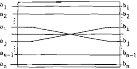
Cell-based interconnection network design 505 An interconnection network is defined as a switching box with N inputs and N outputs. There is a one-to-one correspondence between each input and each output at a fixed instance of time.
It is clear from the above definition that there are in total N! different output permutation patterns of such a box. If the box is constructed using a single switch- ing module only, then it is obvious that the switching module must be able to provide all the N! different permutations. In general, such a module is too compli- cated to construct. Now, if the box is constructed by cascading several (be they the same or different) switching modules successively, then the permutation capability for each module can surely be reduced to a large extent. From the above dis- cussions, the problem that we are concerned with can now be stated as follows:
Find some (say m) distinct exchanging functions with which the whole N! pos- sible permutation patterns can be generated by cascading several stages (say n) of the m patterns in different orders.
It is clear that the solution (m and n) to the above problem is not unique.
In order to meet the requirement for modular deisgn. the permutation capability is chosen to be the same for each module in the proposed network. In other words, m is always fixed. So now, the interconnection problem becomes:
To generate all the N! permutations by using the m given exchanging functions. (Of course, the number of stages, n, must as small as possible to minimize the hardware cost for the real implementation.)
Figure 1 shows the basic 'switching box' mentioned above. The behaviour of this box is described by the corresponding permutation (or switching) matrix P. The entries of P, P i j , are defined as certain functions of the data transfers from position
a, (input) to position bj (output) and from aj to b, at the same time, i.e.
1 if ai -t b j and aj + bi
P . =
{
'' 0 otherwise where -t denotes 'transfer to'.
Since the data transfers between the inputs and outputs are restricted to be 'one-to-one', in P there is only one non-zero element in each row and in each column. Further as a,
-.
bj and a j -+ b, occur simultaneously, P is a symmetric matrix. Under this definition, for an Nth order (with N inputs and N outputs) switching box, there are C: exchanging patterns p i j , where 1<
i, j<
N and i # j.an-1
1
b n - 1!
b"Figure 1. Basic switching box.
506 Ja-Ling Wu
Note that
Bij
is also a permutation matrix and its entries are defined as1 for i # j
for all k # 1 and k # j
otherwise where E(x) denotes 'the entry of x'.
In this case, m = C r , and the least upper bound of n can be derived on the basis of the following lemma.
Lemma 1
If all the C: exchanging patterns are chosen to be candidates for the exchanging functions of the basic cell, then the maximal number of stages n selected for the permutation module is N
-
1.Proof
In this case, for any path from a, to b, there always exists an exchanging pattern,
P,s, which can implement such a data transfer, So, intuitively, at most N stages are required for an Nth order box. But actually, after passing the (N - 2)th stage, (N
-
2) inputs have been connected to the correct output positions. And the last two input can be changed mutually in one stage. So in totalN
- 1 stages, at most, is enough to generate all the N! possible permutations.Example 1
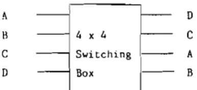
In order to better understand Lemma 1, let us consider a 4th order switching box. From the above lemma, there are C i = 6 basic patterns that can be selected: P12, P13, P14, P23, P24 and P34. By using these 6 patterns we can produce all the
4! (=24) possible permutations. For instance, if the set of data (A, B, C, D) is to be rearranged to (D, C, A, B) through the box, shown in Fig. 2, then some of the possible generation procedures can be given, as in Fig. 3. Note that the sequence of the exchanging patterns is not important in this case.
An (N - 1)-stage cell-based interconnection module/network can now easily be constructed simply by integrating all the C r exchanging patterns into one cell and then duplicating the basic cell N - 1 times. In this approach, the modularity of the network is optimum because only a single basic cell need be designed. However the hardware cost (chip area) of such a network is very high (large) since the control complexity (the number of control signals) for each cell is O(log, C;) = [2 log, N - I], where [x] denotes the least integer that is greater than or equal to x. So an interesting question now arises:
Figure 2. The corresponding switching box of (A, B, C, D) -r (D, C, A, B).
Cell-based interconnection network design
Figure 3. Possible implementations for (A, B, C, D) + (D, C, A, B) in three stages.
Can we construct a cell-based interconnection network with the basic cell whose control complexity is less than [2 log, N -
11
such that the maximal number of stages, is still kept constant ( N - l ) ?In order to answer this question, the definition of the all-pairs examination problem is now introduced:
Given a set of N elements, examine every pair of them; that is, suppose we are
given elements labelled 1 , 2 ,
..
.,
N . Our job is to examine (1, 2), ( 1 , 3),.
.
.,
( 1 , N ) , ( 2 , 3), ( 2 , 4 ) >.
.
.,
(2, N ) (3,4),. .
..
( N - 1 , N ) .Now let us consider the relationship between the all-pairs examination problem and the design of a cell-based interconnection network. Since the inputs of any intercon- nection network can be labelled in a natural order and the outputs are in a permu- tated order, basically, the interconnection or permutation problem can be thought of as a 'backward sorting' problem. In other words, we take the output patterns as the inputs of a sorter, which is constructed using a point-to-point switching box. And as indicated in Lee et al. (1981) the pairwise examination operation has been
successfully applied to solve the sorting problem. Thus suppose one can build up a cell-based network/module to solve the pairwise examination problem and the inter- connection or permutation problem as well.
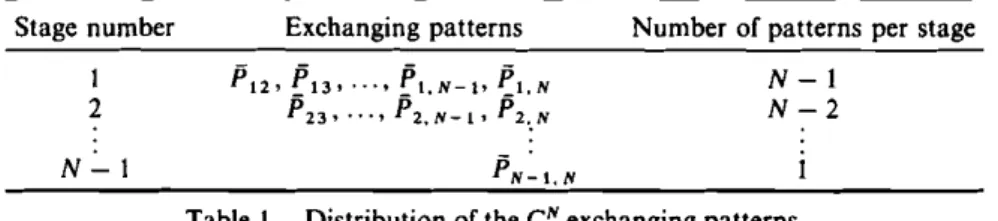
Since there are in total Cf pairwise elements or, equivalently, Cf distinct exchanging patterns need to be examined, and N - 1 stages for our network, why not distribute Cf exchanging patterns into each stage in such a way that the total number of exchanging functions for each cell is less than or equal to N ? In other
words, the control complexity for each stage is made less than or equal to log, N-a reasonable hardware cost.
For the ith stage, the chosen switching functions are simply those exchanging patterns P i j , where j = i
+
1 , i+
2,. .
.,
N . In other words, the switching functionsfor each stage are shown in Table 1 .
The full interconnecting capacity of such a pattern assignment of each stage is obvious (Lee et al. 1981). Since the complexity of each cell is restricted to N , one can
508 Ja-Ling Wu
Stage number Exchanging patterns Number of patterns per stage
Table I . Distribution of the C! exchanging patterns.
easily reduce the number of different cells (or increase the modularity of the network) by merging the switching functions of the ith stage and the ( N - i
+
I)th stage, where i>
1, into one cell and adding the all-pass function Pa, (that isPi,
= 0 for i # j and P i j = 1 for a<
i<
N) to each cell and then symmetrically duplicating along the [N/2]th stage. Now, there are [N/2] different basic cells with N distinct exchanging patterns. The following example explains our approach more clearly.Example 2
Let us design a n 8 x 8 cell-based interconnection module, which is very difficult by the direct analysis approach as indicated in Wu and Lin (1985).
For N = 8 there are in total
C;
= 28 district exchanging patterns and a t most 7stages are allowed. The pattern assignment, in our approach, of each stage is given in Table 2. And after the merge process [8/2] = 4 distinct basic cells are obtained
Stage number Exchanging patterns Number of patterns ~ e r stage
Table 2. Pattern assignment of an 8 x 8 interconnection module
Celllstaee number Exchanging oatterns Number of patterns per staae
Table 3. Basic cells of an 8 x 8 interconnection module.
"* " denotes a cell.
Figure 4. Modified shuming structure.
Cell-based interconnection network design
32 inputs
: basic inlerconnection module
r-., 8 I
I I : bulfer
8 ,
L . . ,
Figure 5. Block diagram of a 32 x 32 interconnection network.
(see Table 3). Each basic cell can be implemented easily by using transmission gate logic (Mead and Conway 1980).
It follows that the control complexity of each cell/stage is 3 (=log, 8) and the total number of stages is 7 ( = 8 - 1). Consequently, the resulting network is a rea-
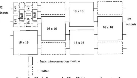
sonable solution to the original design problem. Furthermore, by parallel cascading the above interconnection module in a modified shuming structure, as shown in Fig. 4, then any interconnection network of large size N, where N is divisible by 8, can be obtained systematically. Figure 5 shows a 32 x 32 interconnection network which is constructed by using the proposed 8 x 8 interconnection modules. Note that the buffers are used for the purpose of synchronization and can also be imple- mented using the basic interconnection modules.
The network extension can easily be realized by the same procedure indicated in the above example. From Fig. 5, one can see that there is no line intersections in the intermodular interconnections. In other words, an intersection-free VLSI cell-based interconnection network can be systematically constructed. This property is espe- cially desirable for planar VLSI implementation.
-
-
3. Systematic design procedures for a VLSI cell-based interconnection network Based on the 'pairwise examination' model described in $2, a universal (i.e. highly parallel/pipeline, highly fault tolerant, intersection-free,
. . .
, automatic/self:---1 I 4 L I L - - - . - - - Stage forward 1 2
...
N - 1 N (backward) number (N) (N - 1) (2) (1) - - - '1 PN-tN i 2 . N -'l.N Switching PI, PZZ(:PN-I) Pz. N- I P I . N - Ifunctions P,I 3 Pt3 . . .
. . .
(control patterns) - '23 '13 per stage p ~ A - 1 P2, N - I ' N - I ~ N - I ( = ' * ~ p12- P I , N p2, N PN-I.N PNd=P,,) r - - - I I I 1t-
L-_-.._--..
A 1 6 x 1 6 16 x 16 32 - outputs - - 1 6 x 16 16 x 16,
_ __ _ _ _ _
- - - I I 4 I r I L -... .--- JJa-Ling W u
Figure 6. Symmetric modified shuming structure.
timing and bidirectional) interconnection module/network, with reasonable hard- ware complexity/cost, can easily be constructed by the following two procedures.
Procedure I
Build up an N-stage interconnection module/network with the symmetric switching function (control pattern) assignment given in Table 4.
Procedure I1
The network extension follows the symmetric modified shuffling structure shown in Fig. 6. Each intersection in Fig. 6 denotes an universal interconnection module, defined in Procedure I.
Now, the question is: Is it possible to build a cell-based interconnection network/module with less complexity? In order to answer this question, an effective merging process, which is based on some existing phenomena, is discussed in detail in the next section.
4. Performance improvement by the merging process
As described in $2, network extension follows the modified shuffling structuie as shown in Fig. 4. One can easily show that the following is true.
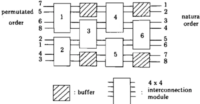
The inputs to each interconnection sub-module, except at the first stage, can be classified into two equal and partially ordered sets. Then, the total possible permu- tation patterns are reduced from N! to N !/N!/2 N!/2; thus the control signals per stage may be reduced as a result of this complexity reduction. For the convenience of our explanation and also as an example, let us considere an 8 x 8 interconnection network which is constructed by cascading 4 x 4 interconnection modules in a modified shuming structure as shown in Fig. 7.
Since the interconnection/permutation problem can be viewed as a 'sorting' problem, the network shown in Fig. 7 can also be viewed as an 8 x 8 sorter. Addi-
1 2 natural order 5 6 7 8 4 x 4 module
Figure 7. 8 x 8 interconnection network (8 x 8 sorter network).
Cell-based interconnection network design Control pattern (switching functions) Permutation
pattern Stage 1 Stage 2 Stage 3
Table 5. Switching functions for the 4 x 4 interconnection modules with partially ordered inputs. (P, denotes the merged switching function of PI, and P,,.)
tionally, if the outputs of the network are defined in natural order and the inputs are in permuted order, then the control signals for each cell can be automatically found by means of software (if they are stored in the RAMS) or they can be directly gener- ated by hardware (after some simple comparisons) following an ascending order. Figure 7 explains this idea very clearly. Note also that, in Fig. 7, cell 1 and cell 2 execute all 4! permutation patterns but cells 3 , 4 , 5 and 6 only execute those permu- tation patterns given in Table 5.
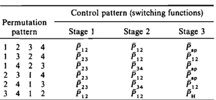
Now if we merge the switching functions PI, and P,, into a new exchanging pattern P,, then the 6 (=4!/2!2!) permutation patterns given in Table 5 can be realized by a two-stage 4 x 4 interconnection module with switching functions as given in Table 6.
Therefore, the interconnection module can be reduced from three stages to only two stages. Thus the network complexity is reduced by a factor of 1.5. In general, this merging process, for large N, needs some computer simulations beforehand. An
0(N2) simulation algorithm for this merging process has been proposed by Lin et al. (1985).
5. Discussion and conclusions
Some applications of the proposed network have been pointed out in Wu and Lin (1985). Above all, the proposed network is a good candidate for the interfacing of processer-processer or processer-memory communications in tightly coupled multiprocesser system.
Control pattern (switching functions) Permutation
vattern Stage 1 Stage 2
Table 6. Switching functions for the two-stage 4 x 4 interconnection module.
512 Cell-based interconnection network design
The cellular design of the proposed network allows very simple intermodule interconnections. This fact results in the most important characteristic of the pro- posed network: there are no line cross-overs between the intermodular intercon- nections. This property is especially desirable for planar VLSI implementation.
REFERENCES
BENTLEY, J. L., and O ~ A N N , T., 1979, Algorithms for reporting and counting geometric intersections. I.E.E.E. Transactions on Computers, 28,64334447.
FENG, TSE-YUN, 1981, A survey of interconnection networks. I.E.E.E. Transactions on Com- puters, 30, 12-27.
FRANKLIN, M. A,, 1981, VLSI performance comparison of banyan and cross-bar communica- tion networks. I.E.E.E. Transactions on Computers, 30,283-291.
GOODMAN, J. W., LEONBERGER, F. J., KUNG, S. Y., and ATHALE, R. A,, 1984, Optical intercon- nections for VLSI systems. Proceedings of the Institute of Electrical and Electronics Engineers, July, 85C865.
HAMBRUSH, A. E., 1983, VLSI algorithms for the connected component problem. S.I.A.M. Journal on Computing, 12,353-365.
HWANG, KAI and BRIGGS, F. A., 1984, Computer Architecture and Parallel Processing (New York: McGraw-Hill).
KUNG, S. Y., WHITEHOUS, H. J., and KAILATH, T., (editors), 1985, V L S I and Modern Signal Processing (Englewood Cliffs, NJ: Prentice Hall).
LEE, D. T., CHANG, H., and WANG, C. K., 1981, An on-chip compare steer bubble sorter. I.E.E.E. Transactions on Computers, 30, 396405.
LIN, TENG-PIN, WU, JA-LING, and CHANG, YANG-TA, 1985, A new moduling of cell-based interconnection network. I.A.S.T.E.D. Conference on Modelling and Simulation, pp.
123- 126.
MEAD, C.. and CONWAY, L., 1980. Introduction to V L S I Systems (Reading, Mass.: Addison- Weslevl. , ,
S E I T Z ; ~ . L., 1984, Concurrent VLSI architectures. I.E.E.E. Transactions on Computers, 33,
1247-1 265.
SHAMOS, M. I., 1976, Geometric intersection problems. Proceedings of the 17th I.E.E.E. Annual Symposium on the Foundations of Computer Science, pp. 208-215.
SHIH. 2. C., CHEN, G. H., and LEE, R. C. T., 1987, Systolic algorithms to examine all pairs of elements. Communications of the A.C.M., 30, 161-167.
Wu, JA-LING, and LIN, TENG-PIN. 1985, A new cell-based interconnection network. Interna- tional Journal of Electronics. 59, 375-382.