低溫多晶矽薄膜電晶體數位電路變動性之模擬研究
55
0
0
全文
(2) photo-detector amplifier [9], scanner, neutral networks [10] and three dimension LSIs [11]. In the future, the application fields of LTPS TFTs will not be limited to displays but will be expanded to other electronic devices, such as LSIs [11], printers and sensors. Among these, the application of poly-Si TFTs in AMLCDs is most noticeable and brings about rapid process in poly-Si TFT technology. Therefore, it is possible to integrate poly-Si TFTs and surrounding driving circuit on the same substrate. This will reduce the assembly complication and the cost dramatically. In addition, since the mobility of poly-Si is higher, the dimension of poly-Si TFTs can be made smaller than that of amorphous silicon ones. This is beneficial to fabricate high density and high resolution AMLCDs.. 1-2. LTPS TFTs Low temperature poly-Si (LTPS) TFT technology appears to be one of the most promising technologies for the ultimate goal of building fully-integrated AMLCD system on glass. The LTPS TFT LCDs achieve high resolution, high luminance displays as well as “System on glass” displays, which allow us to integrate various functional circuits on to the display panels. The so-called system on glass (SOG) TFT-LCD with LTPS technology enables to spare the silicon driver ICs and to enhance the productivity by reducing the module process steps. System-on-panel (SOP) has the merits of high brightness, low power consumption, thin thickness, light weight, fast response, high integration, high reliability, and good image quality. Comparing with the conventional a-Si TFT LCD with silicon ICs on it, the SOG-LCD requires high-performance TFTs such as high carrier mobility (μ), low threshold voltage (VT), and small sub-threshold swing to meet the high speed driving circuits. 2.
(3) that result in good display quality and a small form factor. The LTPS TFT has also the possibility for realizing far more value-added circuit monolithically with the pixels on the array glass. Therefore, the research efforts also have been focused on realization of system integration for LTPS TFT LCDs and have been developed various types of circuit-integrated LCDs so far.. 1-3. Integrated Circuits of System on Panel Fig.1 shows the system block diagram of this panel. As shown in Fig.1, this panel consists of the following seven circuits: the interface circuit to change input logic level to higher level needed for TFT circuitry, the timing generator to generate control pulses for drivers, the reference driver to generate 64-step voltage, the VCOM driver to generate common voltage, the source driver to supply analog voltage to source lines according to input digital signals, the gate driver to select gate lines, and the DC-DC converter to supply negative voltage of gate drivers. The signal processing in the module works with following flows. Data signals are supplied to a driver IC from an external circuit by way of one of the following interfaces (I/Fs) including parallel CPU I/F or serial CPU I/F or RGB I/F. Then the signals are stored to frame memories. Data signals in the frame memories are read out at a constant frequency, and then transferred to D/A converters, which output data to an LCD panel. Output signals include serially composed RGB signals. The most fundamental display driver circuit (for both active- and passive-matrix displays) is the shift register. Assuming the simplest driving scheme, the rows and the columns of the display matrix are activated one by one, which is accomplished by the active shift register output (which can be high or low level signal) being shifted to the next bit, and eventually cycled to the register’s input (Hsync or Vsync) again. When the characteristics of the LTPS TFT are improved by the evolution of the 3.
(4) design rule and processing, the high-speed operation of the circuit becomes possible. It means that shift registers can be operated easily more than MHz.. 1-4. Motivation The method of predicting the yield and power dissipation of digital circuits in VLSI has been extensively studied. In the traditional IC design, Worst Case analysis is the most commonly used technique for considering manufacturing process tolerances on the design of digital integrated circuits. In other words, as soon as we realize the worst component characteristic of transistors, the voltage and operation frequency correspondence of the shift register can be quickly calculated. The frequency decides the resolution of products in the application of system on panel. If one can reduce the voltage, the power can be reduced by a wide margin. However, conventional predictions do not consider the problem of device variation caused by the device characteristics of LTPS TFTs. By the same token, the range of regular voltage corresponding in the maximum frequency, or regular frequency corresponding in minimum voltage may widely distribute over whole circuit design. Generally speaking, the Monte Carlo method used to simulate device variations is quite straightforward. It is also reliable and accurate for all methods used in practice, but for high accuracy, it costs a large computational time. Based on the above, how to develop a front-end simulation skill which quickly and accurately estimates the yield during design phase is became a key point of product competitiveness. To overcome the above problems, we firstly describe the relation between delay time and operation frequency. Moreover, we drive the formula for delay time based on polysilicon TFT RPI model. In chapter 3, we analyze the effects of device 4.
(5) variations in LTPS TFTs digital circuit. The simulation results demonstrate that Vth variation is the most impact factor comparing to the other parameters in LTPS TFTs. A quick simulation skill to save Monte Carlo time will be describe in chapter 4. It is founded that the operation frequency of an n-stage shift register can be obtained through simplifying propagation delay from an n-stage one to an 1-stage one. The power dissipation of an n-stage shift register is also estimated in the same way. The trends of operation frequency correspond to resolution will also be discussed in this chapter. Finally, chapter 5 will give a conclusion on the results obtained.. 1-5. Thesis Organization Chapter 1. 1-1.. Introduction Development of Displays. 1-2. LTPS TFTs 1-3.. Integrated Circuits of System on Panel. 1-4.. Motivation. 1-5.. Thesis Organization. Chapter 2.. Simulation and Analysis Methods. 2-1.. Simulation Methods. 2-2.. RPI Model. 2-3.. Shift Register. 2-4.. Determination of the Delay Time and Operating Frequency. Chapter 3.. The Impact Analysis of Device Parameters. 3-1.. Model Analysis. 3-2.. Monte Carlo Simulation V.S. Formula. Chapter 4.. Simulation Skill. 4-1. Estimation of Operation Frequency 5.
(6) 4-2. Estimation of Power dissipation Chapter 5. 5-1.. Conclusions and Future Works Conclusions and Future Work. References. 6.
(7) Chapter 2 Simulation and Analysis Methods. 2-1. Simulation Methods There are two major methods of simulation to analyze circuit performance, which are the worst-case and Monte Carlo analysis as described below. 2-1-1. Worst-Case Method [1] Worst-Case analysis is the most commonly used technique in industry for considering manufacturing process tolerances in the design of integrated circuits. These approaches are relatively inexpensive compared to the yield maximization approaches in terms of computational cost and designer effort, and they also provide high parametric yields. At any design point, uncontrollable fluctuations in the circuit parameters cause circuit performance to device from their nominal design values. The goal of worst case analysis is to determine the worst values that the performance may have under these statistical fluctuation. In addition to finding the worst-case values of the circuit performance, this analysis also finds the corresponding worst-case values of noise parameters. A noise parameter is treated as a random variable. Any random variable is characterized by probability density function (and by a mean and a standard deviation which depends on the density function), as shown in Fig. 2-1-1. The worst-case noise parameter vector is used in circuit simulation to verify whether circuit performances are acceptable under these conditions. Similar to worst-case analysis, one can also perform best-case analysis. In fact, industrial designs are often simulated under best, worst, and nominal noise parameter conditions, which provide designers with quick estimates of range of variation of circuit performances. 7.
(8) 2-1-2. Monte Carlo Method Yield, expressed as a multi-dimensional integral, can be evaluated numerically using either the quadrature-based, or Monte Carlo based methods. The quadrature-based methods have computational costs that explode exponentially with the dimensionality of the statistical space. Monte Carlo methods, on the other hand, are less sensitive to the dimensionality. The Monte Carlo method is a computer simulation of real distributions of random noise parameters, and it is the simplest, most reliable and accurate of all methods used in practice, but for high accuracy it requires a large number of sample points. Typically, hundreds of trials are required to obtain reasonable accurate yield estimation. For nonlinear and/or time domain circuit analysis, this is computational expensive. Hence, a fundamental problem to solve is to increase the efficiency of the Monte Carlo method and its accuracy, measured by the variance of the yield estimation.. 2-2. RPI Model The poly-Si TFT models could be divided into three categories: the models that try to incorporate the physics related to individual grain boundaries[2], the models that use close form analytical expressions for current-voltage characteristics[3,4], and the models based on effective medium. In recent years, several models for poly-Si TFTs have been proposed. Lin et al. obtained an expression for grain barrier height as a function of gate bias and the lateral electric field from a quasi-two-dimensional formulation of Poisson’s equation. This solution was incorporated in an expression for the drain current in poly-Si TFTs. Further insight relating the characteristics to the poly-Si material parameters was provided by Fortunato and Magliorato [5]. Other solutions use Poisson’s equation with the inclusion of space charge due to traps. Still 8.
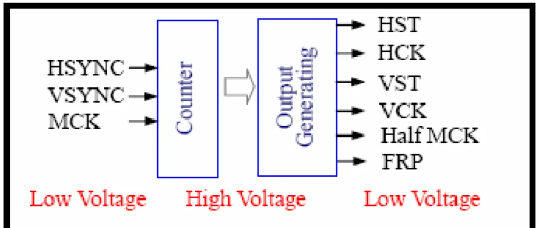
(9) others seek formulations with a minimum of empirical approximations. Although useful for the insight they provide, these expressions tend to be too complication for implementation in circuit simulators. The effective medium approach permits the development of comparatively simple models with only a few easily extractable parameters. Although these parameters cannot always be directly related to material properties, such models are attractive for use in SPICE type circuit simulators. The above models are mainly developed for long-channel poly-Si TFTs although later versions by Jacunski et al. [6,7] have included physics based formulations of important mechanisms such as the kink effect, the field effect mobility in moderate inversion, and the subthreshold current. Finally, the most recent models based on these semi-empirical effective medium approach also include short-channel effects, drain induced barrier lowering (DIBL), velocity saturation, temperature effects, and mobility degradation at high gate bias [6,8-10].. 2-3. Shift Register The most fundamental display driver circuit (for both active- and passive-matrix displays) is a shift register. In this section, we will describe the operation principle of a clocked CMOS (C2MOS) type edge-triggered shift register. 2-3-1. Introduction The periphery circuit blocks of LCD panel are composed of four parts-display panel, timing controller, scan driver and data driver. In Fig. 2-3-1 is the system diagram of the LCD panel driver circuits [11]. Timing controller is responsible for transiting RGB (red, green and blue) signals to data driver and controlling the behavior of scan driver. Generally speaking, TCON (timing controller) is a key element in LCD panel. It 9.
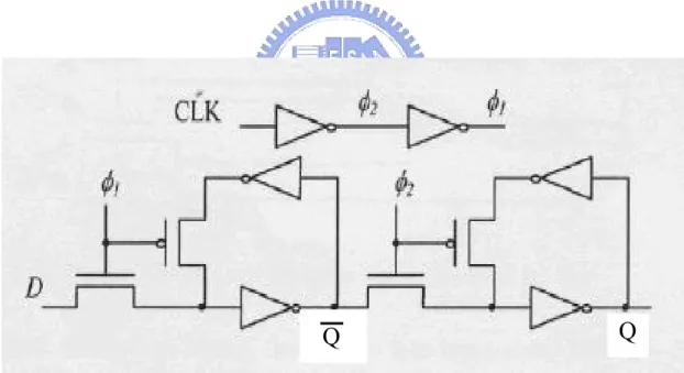
(10) is essentially the brain, the control center, and the heart of a LCD panel. The circuit blocks of timing controller are composed of a counter and an output generating circuit (clocked flip-flops and shift registers), which decodes the output from the counter to generate control signals at corresponding time. Please refer to Fig. 2-3-2 for input and output signals employed. Data driver, shown in Fig. 2-3-3, mainly contains shift register, data latch, level shifter, digital to analog converter and output buffer. Furthermore, the first three parts classify as digital architectures. The other two parts belong to analog architectures. Shift register and data latch manage to transit and store the RGB signals. They must work under higher frequency while operating in higher resolution display. For a 320× 240 QVGA product as an example, if its sweep frequency of scan driver is 60 Hz, the operating frequency of data driver and timing controller will up to 13MHz. 2-3-2. Selection of Shift Register A conventional master-slave D flip-flop [12](type of D-latch shift register) is shown in Fig. 2-3-3. It is composed of two level-sensitive latches. Each latch consists of two CMOS transmission gates and two inverters. The block chain generates the clock signal (φ1) and its inverse (φ2). The total number of transistors used, including the clock chain is 20. To reduce the transistor count, the NMOS or PMOS transmission gate can be used to replace the CMOS transmission gate. Thus, a low power D flip-flop can be constructed as show in Fig. 2-3-4. However, it suffers from the subthreshold currents if there is a voltage difference across the feedback PMOS pass transistor [13,14]. In addition, our experience with NMOS digital circuit such as shift registers and AMLCD line drivers on a polysilicon process has confirmed the disadvantages well know to those involved with crystalline silicon. The power dissipation at low and 10.
(11) medium frequencies is higher because NMOS inverters draw a DC standing current. Furthermore the pull-up enhancement load of a NMOS inverter severely limits circuit performance. At best one can trade off performance with voltage and power dissipation since the load device requires higher gate voltage to maintain speed and voltage swing. Based on the above, it has been said that fewer transistors lead to less power dissipation, but that is not strictly true [15]. Broadly speaking, a D flip-flop consists of the CMOS transistor is the reasonable design for LTPS TFTs. Fig. 2-3-5 shows a different version of the CMOS D flip-flop. Although the circuit appears to be quite different from that show in Fig. 2-3-3 , the basic operation principle of the circuit is the same as that shown in Fig. 2-3-5. The operation of a clocked CMOS (C2MOS) flip-flop will be described below. 2-3-3. Operation of Clocked CMOS (C2MOS) Shift Register The first tristate inverter acts as the input switch, accepting the input signal when the clock is high. At this time, the second tristate inverter is at its high-impedance state, and the output Q is following the input signal. When the clock goes low, the input buffer becomes inactive, and the second tristate inverter completes the two-inverter loop, which preserves its state until the next clock pulse. Considering the two-stage master-slave flip-flop circuit which is constructed by simply cascading two D-latch circuits. The first stage (master) is driven by the clock signal, while the second stage (slave) is driven by the inversed clock signal. Thus, the master stage is positive level-sensitive, while the slave stage is negative level-sensitive. The timing diagram which is shown in Fig. 2-3-6 displays the start pulse and the n-stage output signal.. 11.
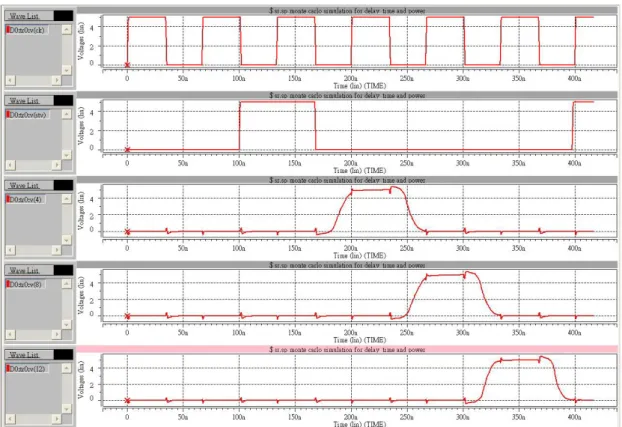
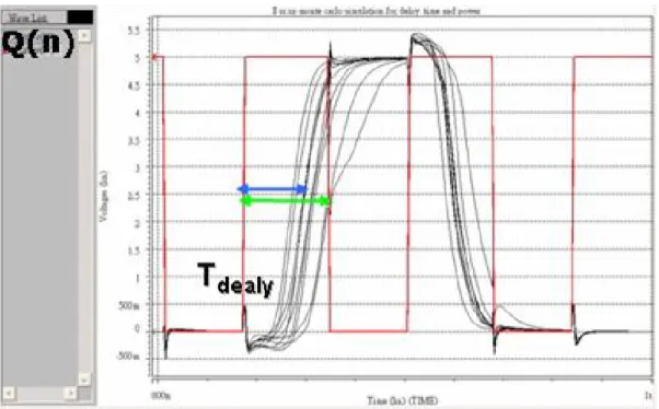
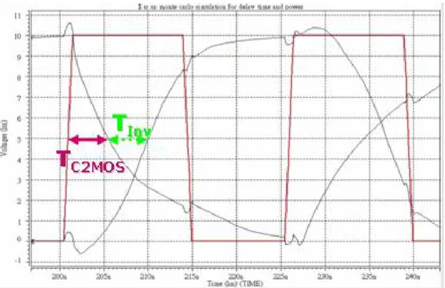
(12) 2-4. Determination of the Delay Time and Operation Frequency Propagation delay has a deep connection with operation frequency. The operating frequency means that of the dot clock (CLK and inversed CLK) when the pulse was not forwarded to the next shift resistor. The maximum clock frequency of a shift register (defined as the maximum frequency for bit error-free operation) depends on the register’s propagation delay and, as such, is a function of device characteristics (e.g., effective mobility and threshold voltage), device geometry (e.g., primarily channel length) and operation conditions (e.g., supply voltage and clock signal levels). Fig. 2-4-1 and Fig. 2-4-2 show the typical simulation results from 1st stage (Q [1]) to 3rd stage (Q [3]) while operating at 15MHz and 19MHz of 5V, respectively. From Fig. 2-4-2, as we have mentioned before, the increase of operation frequency causes the pulse was not forwarded to the next shift resistor. For investigating the transition mechanism of delay effect, a shift register simulation used Monte Carlo method at 15MHz are shown in Fig. 2-4-3 and Fig. 2-4-4. By definition, Tdelay is the time delay between the V50%-transition of the rising/falling clock voltage and V50%-transition of the rising output voltage. The simulation waveforms from nth stage (Q [n]) to (n+1)th stage (Q [n+1]) in Fig. and Fig. display two results. When Tdelay is smaller than 1/2 clock cycles, the signal propagation from forward stage (Q[n]) to next stage (Q[n+1]) can be operated normally. On the contrary, there is showing the failed results for bit error operation, i.e., transition characteristic distortion if Tdelay is larger than 1/2 clock cycles. In fact, Tdelay consists of TC2MOS and TInv ( Tdelay = TC 2 MOS + TInv ). We will refer to Fig. 2-4-5 for the determinations of TC2MOS and TInv. TC2MOS is defined here as the time delay between the V50%-transition of the rising/falling clock voltage and V50%-transition of the falling output voltage of clocked inverter. Similarly, TInv is 12.
(13) defined here as the time delay between the V50%-transition of the falling output voltage of clocked inverter and V50%-transition of the rising output voltage of inverter. We shall have more to say about derivation of Tdelay in next section later on.. 13.
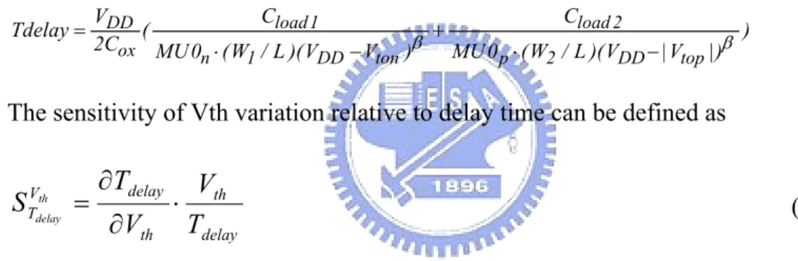
(14) Chapter 3 Impact Analysis of Device Parameters. 3-1. Model Analysis In this section, we firstly start from the equation derivation of Tdelay based on the RPI model of HSPICE. From the equations, we observe that the Vth and mobility are the dominate factors affect the circuit performance. Before simulating, therefore, we have to discuss the distribution device parameters in practice. 3-1-1. Derivation of Delay Time A unified model can be obtained for the drain current (Id) by combining the above-threshold and the subthreshold currents as follows:. 1 1 1 = + I d I sub I a. (3-1). In the operation of digital circuit, the VG always works larger than subthreshold region, that is to say Eq. (3-1) can be written as. 1 1 ≈ . Id Ia. The poly-Si TFT models developed by Jacunski et al.[1] are essentially unified models for long-channel devices. Above threshold (VGT>0), the conducting channel (Ia) in the non-saturated regime and saturation region is given by an expression similar to that used for long-channel crystalline MOSFETs. The transfer I-V characteristics of polysilicon TFT based on HSPICE RPI model [2] can be expressed as. Ia =. µ FET ⋅ Cox ⋅ Weff Leff. 2. (VGT ⋅ VDS. V − DS ) For VDS ≤ α sat ⋅ VGTE 2 ⋅ α sa t 14. (3-2).
(15) Ia =. µ FET ⋅ C ox ⋅ Weff ⋅ VGT 2 ⋅ α sat 2 ⋅ Leff. For V DS ≥ α sat ⋅ VGTE. (3-3). Here, µFET is the gate voltage dependent field-effect mobility that includes the effects of the trap states; Cox=εi/di is the oxide capacitance per unit area, where εi is the dielectric permittivity and di is the thickness of the gate oxide; W and L are the effective gate width and length, respectively; αsat is the body constant; VGT ≡ VGS-VT is the effective extrinsic gate voltage swing, where VGS and VT are extrinsic gate-source voltage and threshold voltage given by the following interpolation function that tends to VDS in the linear regime and to the saturation voltage Vsat in saturation. In poly-Si TFTs, not all charge carriers induced in the channel by the gate voltage will be free to contribute to the drain current. Instead, a significant of the carriers will be captured by traps associated with the grain boundaries, especially near and below threshold. This effect can be taken into account by proposing so-call field effect mobility as follows:. µ FET =. 1 1 + MU 0 µ1 ⋅ ( 2 ⋅ VGTE ) MMU Vsth. (3-4). Where MMU, MU0 and µ1 are extractable mobility parameter. The second term of Eq. (3-4) is the low filed effect of polysilicon TFTs. Assuming the supply voltage is larger than 5V in digital circuit, the low filed effect can be usually neglected, which reduce theαsat value to be 1. Therefore, the drain current I D of polysilicon TFT can be simplified to. [. ]. ID =. 1 W 2 MU 0 ⋅ Cox ⋅ 2(VG − Vto ) − VD For linear region 2 L. (3-5). ID =. 1 W MU 0 ⋅ Cox ⋅ (VG − Vto ) 2 For saturation region 2 L. (3-6). 15.
(16) Obviously, this I-V characteristic is very similar to that in MOSFETs, expect that the mobility and threshold voltage are modified. Once we determine the equations of drain current I D of polysilicon TFT, we will calculate Tdelay by solving the state equation of the output node in the time domain. For deriving the equation of Tdelay, see the definition of propagation delay times. τ PHL. TC 2 MOS =. TInv =. and. τ PLH. [3], then TC2MOS and TInv can be expressed as. 4(VDD − VT ,n ) ⎡ 2VT ,n ⎤ Cload 1 + ln( − 1 )⎥ ⎢ k n (VDD − VT ,n ) ⎣ VDD − VT ,n VDD ⎦. ⎡ 2V ⎤ 4(VDD − VT ,p ) T ,p ⎢ + ln( − 1 )⎥ ⎥ VDD k p (VDD − VT ,p ) ⎢⎢ VDD − VT ,p ⎣ ⎦⎥ Cload 2. (3-7). (3-8). where the first term of delay component in the above equations is obtained during the NMOS/PMOS transistor operates in the saturation region. The second term of delay component is obtained during the NMOS/PMOS transistor operates in the linear region. It is obvious that Eq. (3-6) and Eq. (3-7) are too complex to analyze because of including ln factor in the delay equations. In order to analyze the equations briefly, the first order Taylor’s approximation is used for simplification process, Eq. (3-6) and Eq. (3-7) then can be approximated as Cload1 V TC 2 MOS = DD ⋅ β 2Cox MU 0 ⋅ (W / L )(V n 1 DD − Vton ). (3-8). Cload 2 V TInv = DD ⋅ 2Cox MU 0 ⋅ (W / L )(V − |V |)β p 2 DD top. (3-9). Finally, the complete equation of Tdelay consist of TC2MOS and TInv can be written as. 16.
(17) Cload1 Cload 2 V Tdelay = DD ( ) + β 2Cox MU 0 ⋅ (W / L )(V MU 0 p ⋅ (W2 / L )(VDD − |Vtop |)β n 1 DD − Vton ). (3-10). Thus, we will adopt Eq. (3-10) to discuss the impact sensitivity of the Vth and mobility while operating at a regular frequency. 3-1-2. Distribution of Device parameters. Before simulating, we have to know the distribution of device parameters. In order to examine the distribution of measured data and deviation from the normal distribution, we adopt the histogram, the Q-Q plot (quantile-quantile plots) and the detrend Q-Q plot. The histogram is the most common graph of a frequency distribution. To test the normality of the distribution, the graphical methods include the use of probability plots are develop. These can be either P-P plots (probability-probability plots), in which the empirical probabilities are plotted against the theoretical probabilities for the distribution, or Q-Q plots (quantile-quantile plots), in which the sample points are plotted against the theoretical quantiles. The Q-Q plots are more common because they are invariant to differences in scale and location. If the assumed population is correct, then the observed value and the excepted value for each case would be very close to each other. If the observations come from a specific distribution, then the plotted point should roughly lie on a straight line. On the other hand, if the assumed population is not correct, then the observed and excepted value would not be approximately the same and the points in this plot would not follow the 45o straight line. Thus, if the points in this plot are close to the line of identity, this plot supports the reasonableness of the assumed population distribution. For the same reason, if the plotted points deviate markedly from the line of identity, then the plots also provide evidence that the assumed distribution is not the appropriate model to describe the observed values. Especially for the normal distribution, the Q-Q plots are 17.
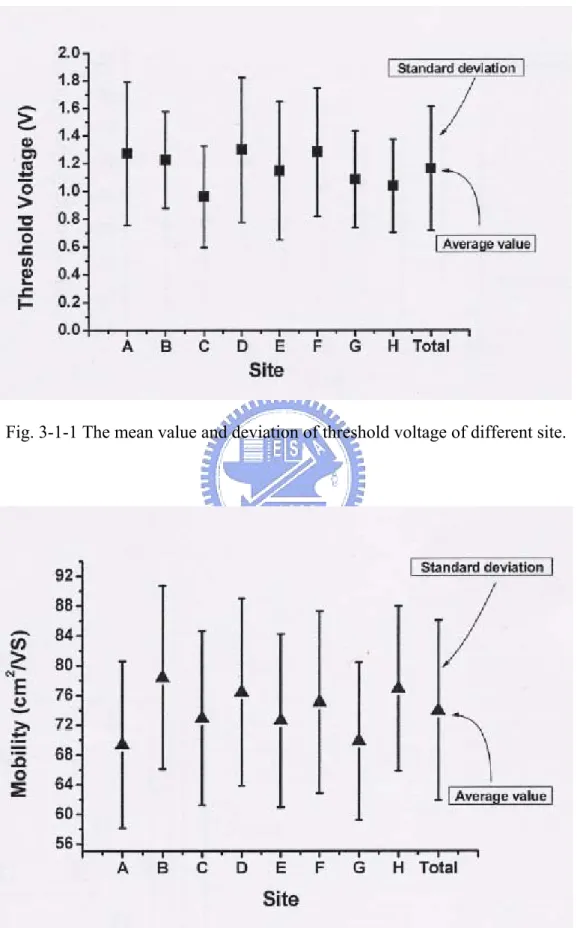
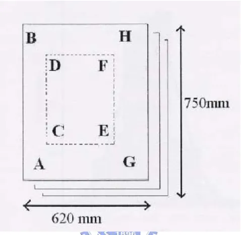
(18) known as the normal probability plots, which are adopted in this thesis. A residual is the difference between an observed value and the corresponding anticipated value. A graphic presentation of residuals, call a residual plot, is useful for highlighting major departures between the observed and the anticipated patterns or relationships in a data set. The detrend Q-Q plot is one of the residual analysis. The residual analysis refers to ser of diagnostic methods for investigating the appropriateness of a regression model utilizing the residuals. If a regression model us appropriate, the residuals should reflect the properties ascribed to the mode error terms ε i . For example, since regression model assumes that the ε i are normal random variables with constant variance, the residuals should show a pattern consistent with these properties. If the model is appropriate, the residuals should reflect the properties ascribed to the model error terms. Using the normal probability plots of the residuals, where the ranked residuals are plotted against their expected values under normality, we may further investigate the difference between the distribution of the measured data and the normal distribution. We first start from the device on different glass. Fig. 3-1-1 and 3-1-2 are the average and deviation values of the threshold voltage and electron mobility of specific device position on different glasses. The relative position of site A to H is defined in Fig. 3-1-3. From Fig. 3-1-1, it can be seen that the average value range of the Vth of these sites is from 0.96V to 1.29V, while the standard deviation range is from 0.33V to 0.52V. The standard deviation of total devices is about 0.446V. Fig. 3-1-4. to Fig. 3-1-9 are the histogram plot, the corresponding Q-Q plot, and the detrend Q-Q plot of, the Vth and mobility. It can be seen that Vth is similar to normal distribution. Refer to the Q-Q plot and the detrend Q-Q plot, the observed values the fitting normal distribution values are both very close. The distribution of 18.
(19) Vth meets our expectation since from the view point of statistical process control, the device parameters should exhibit normal distribution under well-controlled process condition. However, the distribution of mobility shows abnormal distribution based on the Q-Q plot and the detrend Q-Q plot.. 3-2. Monte Carlo Simulation V.S. Sensitivity Analysis To observe the sensitivity of delay, we have two ways to analyze it. The simplest analysis method of sensitivity obtained from derivation of delay equations. Instead, the other method uses Monte Carlo runs. In this section, we will discuss the differences of deviation of delay equations compared with Monte Carlo simulation. 3-2-1. Classical Sensitivity Function. Specifically, for analyzing propagation delay we are usually interested in finding how sensitive their deviations are relative to device variations. These sensitivities can be quantified using the classical sensitivity function S xy , defined. S xy ≡ Lim ∆x →0. ∆y / y ∆x / x. (3-11). Thus. S xy =. ∂y x ⋅ ∂x y. (3-12). Here, x denotes the values of component (e.g., Vth, mobility or swing) and y denotes a circuit a circuit parameter of interest (e.g., propagation delay). We will refer above definition to observe the relationship between device variations and propagation delays. 3-2-1. Simulation Condition. To simulate the sensitivity of propagation delay at a regular frequency the 19.
(20) parameters given in TableⅠvaried one at a time with the rest at nominal value. The threshold voltage parameters VTO and mobility parameters MU0 of N-type and P-type TFTs are +1.5 and -1.5V with the 3σ variation range of ±1.5V, as well as 77.1 and 85 cm2/Vs with the 3σ variation range of ±21cm2/Vs, respectively. One stage shift register is simulated by Monte Carlo method for 100 times with 5V at 1MHz. The width design of inverter is twice of colocked inverter due to the loading of inverter is twice than clocked inverter. Here, the designs of Wn/Wp and L are 4/5 and 6um, respectively. 3-2-2. Vth effect. Here, we rewrite Eq. (3-10) again for convenient derivation of sensitivity. Cload1 Cload 2 V Tdelay = DD ( ) + β β 2Cox MU 0 ⋅ (W / L )(V V ) MU 0 (W / L )(V |V |) − ⋅ − n 1 DD ton p 2 DD top. The sensitivity of Vth variation relative to delay time can be defined as th = S TVdelay. ∂Tdelay ∂Vth. ⋅. Vth Tdelay. (3-13). Thus, the sensitivities of the threshold voltage parameters VTO of N-type and P-type TFTs can be written as ton S TVdelay ∝. V. top S Tdelay ∝. β ⋅ Vton. (3-14). MU 0 n ⋅ (VDD − Vton ). β ⋅ Vtop. (3-15). MU 0 p ⋅ (VDD − Vtop ). Fig. 3-2-1 and 3-2-2 show the dependences of Vth variation on average and deviation delay for Monte Carlo simulation, respectively. From Fig. 3-2-2, it can be seen that the deviation of delay has positive correlation as Vth variation. It seems reasonable to suppose that the Monte Carlo results correspond to Eq. (3-14) and Eq. 20.
(21) (3-15). In addition, we may note, in passing, that the deviation of delay for N-type TFTs is larger than P-type TFTs due to mobility of N-type TFTs is smaller than P-type TFTs. 3-2-3. Mobility effect. In the same way, the sensitivity of Vth variation relative to delay time can be defined as. S Tµdelay =. ∂Tdelay ∂µ. ⋅. µ. (3-16). Tdelay. The sensitivities, therefore, of the mobility parameters MU0 of N-type and P-type TFTs can be written as n STµdelay ∝. µ. p STdelay ∝. 1 MU 0 n. (3-17). 1 MU 0 p. (3-18). To compare simulations with above equations, the Monte Carlo results are shown in Fig. 3-2-3 and 3-2-4. From Fig. 3-2-4, the deviations of delay for 100 Monte Carlo runs show a linear dependence with mobility variations, as exception for above sensitivity equations. It is obvious that the mobility variations of N-type TFTs of delay are also larger than P-type TFTs. 3-2-4. Vth and Mobility Effect. After individually discussing the dependence of Vth and mobility variations on the deviation of delay, now we want to know which one is the most important factor in digital circuit. Fig. 3-2-5 shows the dependences of Vth, mobility and both variations on deviation of delay with 100 Monte Carlo runs, respectively. From Fig. 3-3-5, it can be seen that the triple range of Vth and mobility variations relative to 21.
(22) delay deviation are about 4.5 and 1 nsec, respectively. Moreover, we observe that the deviation value of delay is up to 5 nsec while considering both Vth and mobility variations. The results make it clear that the variation of Vth is more important than mobility in digital circuit. Thus, the simulation of Vth variation will play a impact role on front-end design section.. 22.
(23) Chapter 4 Simulation Skill. From the chapter above, we have described a method to determine operation frequency from delay time, and it is also demonstrated that the Vth variation of device mainly affects circuit performance in whole parameters. In this chapter, we wil propose a simulation skill to predict operation frequency of an n-stage shift register through simplifying propagation delay from an n-stage one to an 1-stage one. The power dissipation of an n-stage shift register is also estimated in the same way.. 4-1. Estimation of Operation Frequency 4-1-1. Worst Case V.S. Monte Carlo. In the chapter 2, we have mentioned that the most frequently used Worst-Case parameters in a practical design are ones that represent “maximum” and “minimum” current of PTFT and NTFT transistors. Because the delay time of cells depend on transistor current, “maximum” and “minimum” parameters correspond to the “fast ” and ”slow” case, respectively. Although Worst-Case is widely used in a practical design, it does not have enough accuracy while comparing with that of a Monte Carlo analysis. Fig. 4-1-1 shows a distribution of gate delay calculated by the Monte Carlo analysis with 1000 SPICE simulations. Two worst-case values calculated by Worst-Case and Monte Carlo analysis are indicated as “corner” and “MC”, respectively. From Fig. 4-1-1, the worst-case rang of the Worst-Case simulation is 19% wider than the range of the Monte Carlo analysis. In order to obtain the high accuracy of Monte Carlo analysis, one has to develop simulation skills to save 23.
(24) simulation time. 4-1-2. One-Stage Shift Register. Over the past few years, several studies [2,3] have been conducted on future application potential of LTPS TFT LCD display. Some of the most compelling studies have focused on typical simulation of an one-stage shift register. For example, Fig. 4-1-2 shows the operating frequency of a shift register simulated as a function of variations in the field effective electron mobility and channel length. The results show the interesting trends while designing LTPS TFTs digital circuits, e.g. , when a timing controller with a 3V voltage source is integrated into LCD panel whose resolution is VGA (25 MHz dot clock), the electron mobility of an N-type TFT higher than 200 cm2/Vs and channel length shorter than 2um for the TFT characteristics are needed. However, little attention has been given to the estimation of delay with device variations. Let us begin with the observation of one-stage simulations for Monte Carlo method compared with typical method. The trend of operation frequencies of one-stage shift register with different supply voltages were investigated by means of Monte Carlo and Worst Case simulations using Vth ± 3σVth, as shown in Fig. 4-1-3. From Fig. 4-1-3, the typical result obviously over-estimating than Monte Carlo results. It is said that one-stage simulations have an advantage in predicting operating frequency in LTPS TFTs digital circuits. However, there seems to be no established theory to explain this trend. In digital circuits a path delay is one of the most important performances, so that it is necessary to analyze the variability of the path delay. In next section, we will now discuss the derivation of path delay from one-stage to n-stage shift register more closely.. 24.
(25) 4-1-3. N-Stage Shift Register. First of all, we will focus our attention on deviation of path delay [1]. The probability distribution function pdf of gate delay can be modeled by an normal distribution function N (m, σ 2 ) fully characterized by its mean value and its variance. σ 2 = (σ delay ) 2 by − 1 −0.5[( d delay − d delay ) 2 /(σ delay ) 2 ] ⋅e 2π ⋅ σ delay. f (d delay ) =. (4-1). where σ delay is defined as the deviation of half-stage delay The average delay of a path comprising n stages corresponds to the linear combination of the n pdfs of the gate delays. The average path delay is given by −. n. d path = ∑ d delay i. (4-2). i. With the symmetrical covariance matrix C ~. C= ~. c11 c 21 ... c n1. ... c1n ... c 2 n ... ... ... c nn. and. cij = σ delayei ⋅ σ delay j ⋅ ρij. cii = σ 2 delay i. (4-3). ρ ij : correlation between two different half-stages the variance of the path can be expressed as n. n. i. j. (σ path ) 2 = ∑∑ σ delaye i ⋅ σ delay j ⋅ ρ ij. (4-4). 25.
(26) n. n. i. j. = ∑∑ cij = e T ⋅ C ⋅ e [4]. (4-5). ~. Equation (4-5) can be simplified to For ρ ij = ρ , i.e., the integrate correlation is the same for all half-stages n. n. n. i. j. i. (σ path ) 2 = ∑∑ σ delaye i ⋅ σ delay j ⋅ ρ + ∑ (1 − ρ ) ⋅ (σ delaye i ) 2. (4-6). The distance dependent correlation of the gate delay on the chip is given by the autocorrelation coefficient ρ [5]. As the device variations of each shift register have no relevance to distance, i.e., the device variation is independent to distance. The autocorrelation coefficient ρ can be set to ρ = 0 . Here, with the variance of a half-stage shift register σ delayi , the variance of a path comprising n gates is given as 2. n. σ 2 path = ∑ σ 2 delay i. (4-7). i =1. It will be clear from Eq. (4-7) that the variance of a path comprising n half-stages is the linear combination of each half-stage delay. Fig. 4-1-4 shows the average and deviation delays of different nth half-stage on delay time with 30 Monte Carlo simulations. From Fig. 4-1-4, it is seen that the device variations correspond to different deviation of delays. σ delay i are similar to each other. Thus, Eq. (4-7) can be. approximated to. σ. 2. n. path. = ∑ σ 2 delay. (4-8). i =1. Finally, as mentioned that the determination of operation frequency determined in chapter 2, operation frequency finally can be written as. 26.
(27) F=. 1. (4-9). 2 ⋅ (mdelay + σ path ). where m is described as mean value with Monte Carlo results of an half-stage shift register. The trend of operation frequencies composed of various n half-stage shift registers with different supply voltages were calculated by Eq. (4-9). The results are shown in Fig. 4-1-5. It was found from the results that operating frequencies showed a reduced ration. 1. n. while gradually increasing half-stage numbers.. 4-2. Estimation of Power Dissipation The histogram of the power dissipation for the good cases is shown in Fig. 4-1-6, which exhibits normal distribution. This Monte Carlo approach is believed to give better approximation to the actual circuit performance for LTPS TFTs because that it makes no restrictive assumptions on the nature of the relationship between the circuit parameters and the circuit performance. As for the power consumption, after excluding the failed cases, the linearly product method can be applied, as shown in Table Ⅱ. That is, the power distribution of an n-stage shift register circuit (PEn) can be estimated by the results of Monte Carlo simulation for 3-stage shift register (PMC3) Average (PEn) = Average (PMC3) × n. /3. (4-10). and Deviation (PEn) = Deviation (PMC3) ×. n /3. respectively.. 27. (4-11).
(28) The comparison between PE20 and PMC20 at 10, 11, and 12MHz is listed in Table II. For the frequencies with enough good cases, the errors for the average and deviation are as low as 3% and 8%, respectively.. 28.
(29) Chapter 5 Conclusions and Future Work. In this thesis, we investigate the device variation issue in the LTPS TFTs digital circuit. A propagation delay is one of the most important performances, so that it is necessary to analyze the variability of the propagation delay. Firstly we aim at the reason causes the shift register circuit to fail with Monte Carlo simulations. By analyzing the variance of transition characteristic with respect to device variation, we determine the equations of propagation delay corresponds to clock operation frequency. At the same time, we derive the equation derivation of Tdelay in detail based on the RPI model of HSPICE. Next we examine the distributions of threshold voltage and mobility variations from different glasses by adopting statistical analysis method with the histogram, the Q-Q plot and the detrend Q-Q plot. It is observe that the distributions of threshold voltage and mobility are the normal and random distributions, respectively. Thus, the Gaussian function of Vth and random function of mobility parameters in the models will be simulated by SPICE. For discussing the sencitivity of Vth and mobility variations on delay compared with Monte Carlo simulation. We start form classical sensitivity function to derive the sensitivity equations of threshold voltage and mobility variations on Tdelay. The results of the dependences of Vth and mobility variations on average and deviation delay for Monte Carlo simulations are in agreement with the sensitivity equations. Moreover, we also observe the results make it clear that the Vth variations cause the variances of digital circuit are larger than mobility. 29.
(30) For predicting circuit performance, we proposed a simulation skill to save computational time with Monte Carlo simulation. It is founded that the operation frequency of an n-stage shift register can be obtained through simplifying propagation delay from an n-stage one to an 1-stage one. The power dissipation of an n-stage shift register is also estimated in the same way. For the frequencies with enough good cases, the errors for the average and deviation are as low as 3% and 8%, respectively. From the viewpoints of circuit performance, the variation of device behavior will lead to extra difficulties in prediction. From the scope of statistics, the database of variability can be constructed with different device distance so that one can predict the fluctuation range of device parameter as the device distance is known. In our work, we have classified and quantitatively distinguished macro and micro variation. This would be helpful for designers in predicting the circuit performance and device reliability. We also, furthermore, have to investigate low voltage digital circuit correspond to low field effect before LTPS TFTs can be widely adopted in flat panel display.. 30.
(31) References. Chapter 1 [1.1] Y. Nakajima, “Latest Development of "System-on-Glass" Display with Low Temperature Poly-Si TFT,” SID, p864, 2004. [1.2] H. Oshima and S. Morozumi, “Future trends for TFT integrated circuit on glass substrate,” IEDM Tech. Dig., 157, 1989. [1.3] H. Kuriyama et al., “An asymmetric memory cell using a C-TFT for ULSI SRAM, ” Symp. On VLSI Tech., p38, 1992. [1.4] S. D. S. Malhi, H. Shichijio, S.K. Banerjee, R. Sundaresan, M. Elahy, G. P. Polack, W. F. Richardaon, A. h. Shah, L. R. Hite, R. H. Womoack, P. K. Chatterjee, and H. W. Lan, “Characteristics and Three-Dimenssional Integration of MOSFETs in Small-Grain LPCVD Polycrystalline Silicon,’’ IEEE Trans. Electric Devices, Vol.32, No.2, pp.258-281, 1985. [1.5]. N. D. Young, G. Harkin, R. M. Bunn, D. J. McCullloch, and I.D. French, “The. Fabrication and Characteristization of EEPROM Arrays on Glass Using a Low-Temperature Poly-Si TFT Process,’’ IEEE Trans. Electron Devices, Vol. 43, NO.11, pp.1930-1936, 1996. [1.6] K. YoShizaki, H. Takahashi, Y. Kamigaki, T.Yasui, K. Komori, and H. Katto, ISSCC Digest of tech. Papers, p.166, February 1985. [1.7] T. Kaneko, Y. Hosokawa, M. Tadauchi, Y. Kita, and H. Andoh, “400 dpi Integrated Contact Type Linear Image Sensors with poly-Si TFT’s Analog Readout Circuits and Dynamics shift Registers,” IEEE Trans. Electron Devices, Vol.38, No.5 ,pp.1086-1039,1991. 31.
(32) [1.8]. Y. Hayashi, H. Hayashi, M. Negishi, T. Matsushita, “A Thermal Printer Head. with Cmos Thin-Film Transistors and Heating Elements Integrated on a Chip,’’ IEEE Solid-State Circuits Conference (ISSCC), p.266, 1998. [1.9]. N. Yamauhchi, Y. Inaba, and M. Okamamura, “An Integrated. Photodector-Amplifier using a-Si p-i-n Photodiodes and Poly-Si Thin Film Transistors, ’’ IEEE Photonic Tech. Lett., Vol.5, p.319, 1993. [1.10] M. G. Clark, “Current Status and Future Propects of Poly-Si,’’ IEEE proc. Circuits Devices Syst., Vol. 141, No.1, p3.3, 1994. [1.11]. K. Nakazawa, J. Appl. Phys., 69(3), pp.1703, 1992.. Chapter 2 [2.1] J. C. Zhang, M. A. Styblinski, “Yield and variability optimization of integrated circuits,” Kluwer Academic Publishers, 1995 [2.2] P.-S. Lin, J-Y. Guo, and C.-Y. Wu, “A Quasi-Two Dimensional Analytical Model for the Turn-On Characteristic of polysilicon Thin-Film Transistors,’’ IEEE Trans. On Electron Devices, 37 (3), 666-674 (1990). [2.3] S. Chen, F. Shone, and J. Kuo, “A closed form inversion type polysilicon thin-film transistor DC/AC model consonsidering the kink effect,’’ J. Appl. Phys., 77, 1776(1995). [2.4]. H. Chern, C. Lee, and T. Lei, “An analytical model for the above threshold. characteristics of polysilicon thin-film transistors,’’ IEEE Trans. Electron Devices, 42, 1240(1995). [2.5]. G. Fortunate and P. Migliorato, ”Model for the abovethreshold characteristics. and threshold voltage in polysilicon thin-film transistors,” J. Appl. Phys., 68, 32.
(33) 2463(1990). [2.6] M. Jacunski, “Characterization and Modeling of Short-Channel Polysilicon Thin Film Transistors,’’ Ph. D. Dissertation University of Virginia, 1997. [2.7] M. Jacunski, M. shur, and A. A. Owusu, T Ytterdal, M. Hack, and B. iniguez, “A Short Channel DC SPICE Model for Polysilicon Thin Film Transistors Including Temperature Effects,’’ IEEE Trans. on Electron Devices, 46(6), 1146-1158(1999). [2.8] S. S. Sung, D. C. Chen, C. T. Cheng and C. F. Yeh, “ A physically-Based Built-in Spice Poly-Si TFT Model for Circuit Simulation and Reliability Evaluation,’’ Proceedings of IEDM, 139-142, December 1996. [2.9] M. D. Jacunski, M. shur, T. Ytterdal, A OWusu, and M. Hack, “AC and DC Characterization and SPICE Modeling of Short-Channel Polysilicon TFT’s,’’ presented at 1996 Mater. Res. Soc. Spring Meet., San Francisco, Ca., Apr. 1996. [2.10]. B. Iniguez, Z. Xu, T. A. Fjeldly, and M. Shur, “Unified Model for. short-Channel Poly-Si TFTs,’’ Solid-State Electronics, 43, 1821-1831(1999). [2.11]. Y. Kida, Y. Nakajima, M. Takatoku, M. Minegishi, S. Nakamura, Y. Maki. and T. Maekwa, “A 3.8 inch Half-VGA Transflective Color TFT-LCD with Completely integrated 6-bit RGB Parallel Interface Drivers,” EURODISPLAY, p. 831, 2002. [2.12]. S. M. Kang, Y. Leblebigi, “CMOS Digital Integrated Circuits,”. McGRAW-Hill International Editions, 1999. [2.13]. G. M. Blair, “Low-power double-edge triggered flip-flop,” Electron. Lett.,. 33, pp. 845-847, 1997. [2.14]. R. Hossain, L. D. Wronski, and A. Albicki, “Low power design using double. edge triggered flip-flops,” IEEE Trans. VLSI Syst. 2, pp. 261-265, 1994. 33.
(34) [2.15] L. Po and O. G. Ling, “Low-power and low-voltage D-latch,” Electronic Letters, Vol. 34, No. 7, 1998.. Chapter 3 [3.1] M. Jacunski, “Characterization and Modeling of Short-Channel Polysilicon Thin Film Transistors,’’ Ph. D. Dissertation University of Virginia, 1997. [3.2] [3.3]. RPI Polysilicon-Si TFT Model (Level=62), HSPICE Manual, 2004. S. M. Kang, Y. Leblebigi, “CMOS Digital Integrated Circuits,”. McGRAW-Hill International Editions, 1999.. Chapter 4 [4.1] M. Eisele, J. Berthold, D. S. Landsiedel, and R. Mahnkopf, “The impact of Intra-die device parameter variations of path delays and on the design for yield of low voltage digital circuits,” IEEE Trans. VLSI Syst., Vol. 5, No. 4, 1997. [4.2]. S. M. Fluxman, “Design and performance of digital polysilicon. thin-film-transistor circuits on glass,” IEE Proc. Circuit Syst., Vol. 141 No.1, 1994 [4.3]. K. Yoneda, R. Yokoyma and T. Yamada, “Future Application Potential of. Low Temperrature p-Si TFT LCD Displays,” SID, 2001 [4.4]. R. Johnson and D. Wichern, “Applied Multivariate Statistical Analysis,”. Englewood Cliffs, NJ, Prentice-Hall, 1982. [4.5]. G. Box, W. Hunter, and J. Hunter, “Statistics for Experiments,” New York,. Wiley, 1978.. 34.
(35) Fig. 2-1-1 Probability density function for (a) a Gaussian and (b) a uniform random variable.. Fig. 2-3-1 System Block Diagram. 35.
(36) Fig. 2-3-2 Block diagram of Timing Controller. Fig. 2-3-3 Block diagram of Data driver. 36.
(37) Q. Q. Fig. 2-3-3 The master-slave D flip-flop (version 1). Q Fig. 2-3-4 The original low-power D flip-flop. 37. Q.
(38) Fig. 2-3-5 CMOS implementation of the D-latch (version 2). Fig. 2-3-6 Time diagram of shift register. 38.
(39) Fig. 2-4-1 Output simulation waveforms of supply voltage 5V, at 15MHz. Fig. 2-4-2 Output simulation waveforms of supply voltage 5V, at 19MHz. 39.
(40) Fig. 2-4-3 Monte Carlo simulation results of n-stage shift register, at 15MHz. Fig. 2-4-4 Monte Carlo simulation results of n+1-stage shift register, at 15MHz. 40.
(41) Fig. 2-4-5 Tdealy consists of TC2MOS and TInv. 41.
(42) Fig. 3-1-1 The mean value and deviation of threshold voltage of different site.. Fig. 3-1-2 The mean value and deviation of mobility of different sites 42.
(43) Fig. 3-1-3 The relative position of the eight sites. 43.
(44) Fig. 3-1-4 The histogram of Vth of horizontal crosstie devices.. Fig. 3-1-5 The Q-Q plot of Vth of horizontal crosstie devices.. 44.
(45) Fig. 3-1-6 The detrended Q-Q plot of Vth of horizontal crosstie devices.. Fig. 3-1-7 The histogram of mobility of horizontal crosstie devices. 45.
(46) Fig. 3-1-8 The Q-Q plot of mobility of horizontal crosstie devices.. Fig. 3-1-9 The detrended Q-Q plot of mobility of horizontal crosstie devices.. 46.
(47) Table I Parameter values and ±3σ variations NTFT. Parameters. PTFT. value. distribution. value. distribution. Vth (V). 1.5±1.5. Gaussian Normal. -1.5±1.5. Gaussian Normal. Mobility (cm2/vs). 77.1±21. Random. 85±21. Random. 47.
(48) Fig. 3-2-1 Vth variation dependence on the average of delay time. Fig. 3-2-2 Vth variation dependence on the deviation of delay time. 48.
(49) Fig. 3-2-3 Mobility variation dependence on the average of delay time. Fig. 3-2-4 Mobility variation dependence on the deviation of delay time. 49.
(50) Fig. 3-2-5 Vth and mobility variations dependence on the deviation of delay time x:0.5 V standard Deviation of Vth 7 cm2/vs distribution range of mobility. 50.
(51) Total samples 1000 Corner. MC. Fig. 4-1-1 Histogram of an inverter circuit carries delay and its worst-case values. Fig. 4-1-2 Result of Shift Register Simulation (VDD=3V) 51.
(52) Fig. 4-1-3 The trend of operation frequencies of one-stage shift register with different supply voltages were investigated by means of Monte Carlo and Worst Case simulations using Vth ± 3σVth. 52.
(53) STV. Half. Half. SR1. SR2. Q(2). Half. Half. SR3. SR4. Q(4). Half. Q(16) Half. SR16. Q(32). SR32. Total 30 samples. Delay Time (ns). 19. σ delay i. 18 17. mdelay i. 16 15 14. 0. 4. 8. 12. 16. 20. 24. 28. 32. Q(n). N Half-Stages Operation Frequency (MHz). Fig. 4-1-4 The average and deviation delays of different single stages on delay time. 50. 3σ. 2 Half-Stages 8 Half-Stages 16 Half-Stages 32 Half-Stages 120 Half-Stages. 40 SVGA. 30. (40MHz. 20. 1 N. 10. 0. VGA (25MHz). QVGA. 5. 6. 7. 8. 9. 10. (6MHz). VDD (V). Fig. 4-1-5 The trend of operation frequencies of n stage shift registers with different supply voltages. 53.
(54) Fig. 4-1-6 The histogram of the power dissipation for the good cases. 54.
(55) Table Ⅱ Power Estimation for 20-stage SR Circuit. 55.
(56)
數據

+7

相關文件
External evidence, as discussed above, presents us with two main candidates for translatorship (or authorship 5 ) of the Ekottarik gama: Zhu Fonian, and Sa ghadeva. 6 In
With the proposed model equations, accurate results can be obtained on a mapped grid using a standard method, such as the high-resolution wave- propagation algorithm for a
If x or F is a vector, then the condition number is defined in a similar way using norms and it measures the maximum relative change, which is attained for some, but not all
• To introduce the use of the LPF as a tool for planning the school English Language curriculum; and
Understanding and inferring information, ideas, feelings and opinions in a range of texts with some degree of complexity, using and integrating a small range of reading
ASL arithmetically shift a memory location left by one bit ASLA arithmetically shift the accumulator left by one bit ASLX arithmetically shift the index register left by one bit
As a byproduct, we show that our algorithms can be used as a basis for delivering more effi- cient algorithms for some related enumeration problems such as finding
First, in the Intel documentation, the encoding of the MOV instruction that moves an immediate word into a register is B8 +rw dw, where +rw indicates that a register code (0-7) is to
Operating mode After SCAN_N has been selected as the current instruction, when in SHIFT-DR state, the scan chain select register is selected as the serial path between TDI and
