Trimethylchlorosilane Treatment of Ultralow Dielectric
Constant Material after Photoresist Removal Processing
T. C. Chang,a,c,
*
,zY. S. Mor,bP. T. Liu,cT. M. Tsai,bC. W. Chen,bC. J. Chu,d F. M. Pan,c,
*
W. Lur,eand S. M. Szeb,ca
Department of Physics, National Sun Yat-Sen University, Kaohsiung, Taiwan bInstitute of Electronics, National Chiao Tung University, Hsin-Chu, Taiwan c
National Nano Device Laboratory, Hsin-Chu 300, Taiwan dNanmat Technology Company, Kaohsiung, Taiwan e
United Microelectronic Corporation, Hsin-Chu, Taiwan
The dielectric properties of organic-porous silica films deteriorate after photoresist removal processing. O2plasma ashing has been commonly used to remove photoresist. Nevertheless, the O2plasma will destroy the functional groups and induce moisture uptake in porous silica films. In this study, trimethylchlorosilane共TMCS兲 is used to repair the damage to porous silica caused by the O2 plasma ashing process. The leakage current and dielectric constant will decrease significantly after the TMCS treatment is applied to damaged porous silica. These experimental results show that the TMCS treatment is a promising technique to repair the damage to porous silica during photoresist removal processing.
© 2002 The Electrochemical Society. 关DOI: 10.1149/1.1504456兴 All rights reserved.
Manuscript submitted September 4, 2001; revised manuscript received April 2, 2002. Available electronically August 29, 2002.
As ULSI共ultralarge-scale integration兲 circuits are scaled down to the deep submicrometer regime, interconnect delay becomes in-creasingly dominant over intrinsic gate delay. In order to reduce the resistance-capacitance delay time, using low dielectric constant 共low-k兲 materials as intermetal dielectrics is one of the effective methods. In addition, the use of low-k dielectrics can also lower power dissipation and reduce cross talk noise.1-3
There are numerous low-k dielectric materials available with the dielectric constant in the range of 2.0-4.1.4-10Within many low-k dielectrics, nanoporous material is a promising candidate. It has be-come an important class of low-k materials because the incorpora-tion of voids reduces the dielectric constant of the film by lowering the overall material density.11-13Organic porous silica共sample STD兲 one of the nanoporous materials, is a good candidate for ULSI ap-plications because of the low dielectric constant of about 2.0. There-fore, integrating porous silica as an interlayer dielectric into multi-level interconnects has received much attention in recent years.
However, photoresist stripping is an indispensable step in inte-gration processing. Photoresist removal is commonly implemented with O2plasma ashing. The dielectric properties of the porous silica will deteriorate during photoresist stripping processes.14,15For over-coming the process issue, we have studied the trimethylchlorosilane 共TMCS兲 treatment to improve the quality of porous silica film. Elec-trical measurement and material analyses have been used to evaluate porous silica. In addition, O2plasma ashing has been investigated to realize the impact of integrated processes on the dielectric film quality.
Experimental
The porous silica films used (CH3SiO1.5) contain methyl groups. The material has been developed by increasing the number of the methyl group thus giving a hydrophobic surface and resulting in lower film polarity. In addition, the porosity 共volume fraction of pores兲 of the silica is about 50% and this leads to a low dielectric constant; a value of k⫽ 1.9 was achieved.
The unpatterned silicon wafers were coated with the porous silica solution at a rotational velocity of 3000 rpm for 20 s. Then, the sequential bake was in the furnace under nitrogen atmosphere. For the bake condition, the temperature was raised from room tempera-ture to 425°C at a rate of 20°C/min. Finally, the resulting wafers were further processed by furnace curing at 425°C for 60 min.
In this work, samples STD, A, and B were prepared. Sample STD was the as-cured porous silica film without any plasma treat-ment. Sample A was the as-cured porous silica with O2 plasma ashing for 30 s. Sample B was the O2plasma-treated porous silica
共sample A兲 after undergoing TMCS atmosphere at 60°C for 15 min. Afterward, all of the samples were further processed by furnace curing at 400°C for 60 min. Finally, aluminum was deposited on samples STD, A, and B as the top electrode to manufacture the metal insulation semiconductor共MIS兲 structure.
The O2 plasma ashing was carried out in a plasma-enhanced chemical vapor deposition共PECVD兲 chamber. The O2plasma was operated with an rf power of 200 W at a pressuse of 300 mTorr. The flow rate was 700 standard cubic centimeters per minute, and the operating temperature was kept at 300°C.
The TMCS treatment was performed by utilizing TMCS vapor to treat sample A in an oven. The TMCS vapor is generated by heating TMCS solution and the vapor is conveyed to the oven at 60°C. Moreover, the TMCS vapor treatment is carried out at a pressure of 760 Torr.
The chemical structure of the porous silica following different processing was investigated by Fourier transform infrared 共FTIR兲 spectroscopy. The thickness of the porous silica was measured by an n & k analyzer. A Keithley model 82 cyclic voltammetry meter was used to measure the dielectric constant of porous silica, and the capacitance-voltage characteristic was measured at 1 MHz with an ac bias for high frequency. Finally, the current-voltage characteristic was also measured by using MIS structure to evaluate the insulation property of porous silica.
Results and Discussion
In the integrated processes, the photoresist removal is imple-mented conventionally by utilizing the O2plasma ashing to remove organic photoresist. However, porous silica has a large exposed-surface area. This will raise the opportunity of reaction between porous silica and the O2plasma when porous silica undergoes pho-toresist removal. Therefore, the impact of the O2plasma processing on the porous silica film must be investigated.
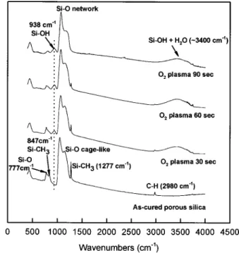
Figure 1 shows the FTIR spectra of sample STD after being subjected to O2plasma ashing for 30 to 90 s. The intensities of the Si-OH and H2O 共938, ⬃3400 cm⫺1兲 signals increase when O2 plasma ashing is applied to sample STD. Furthermore, the intensi-ties of Si-C共847, 1277 cm⫺1兲 peaks and C-H (2980 cm⫺1) peak are decreased dramatically. This indicates that oxygen radicals can diffuse deeply into porous inner structure of organic silica to attack a large amount of Si-C and C-H groups. This will lead to a large *Electrochemical Society Active Member.
zE-mail: tcchang@ndl.gov.tw
Journal of The Electrochemical Society, 149共10兲 F145-F148 共2002兲
0013-4651/2002/149共10兲/F145/4/$7.00 © The Electrochemical Society, Inc.
F145
) unless CC License in place (see abstract). ecsdl.org/site/terms_use
address. Redistribution subject to ECS terms of use (see 140.113.38.11
number of Si-C and C-H bonds breaking, leaving many dangling bonds in the film. In addition, it is considered that two factors might cause an increase of the Si-OH groups. One is that when the O2 plasma attacks the Si-CH3 groups, porous silica immediately ab-sorbs oxygen radicals to convert Si-CH3units to Si-OH groups. The other is that the dangling bonds in the porous silica absorb moisture immediately when the sample is exposed to the atmosphere. As a result, the functional groups in porous silica will be destroyed by the oxygen radical attack when the porous silica is exposed to O2 plasma ashing. This will lead to the decreasing content of methyl
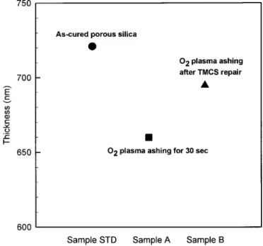
groups in porous silica so that the film thickness will decrease. The thickness variation has confirmed our inference. The thickness is decreased with an increase of the O2 plasma treatment time, as shown in Fig. 2.
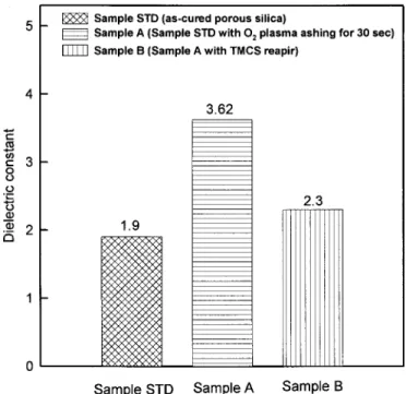
Porous silica with an excellent low-k property is due to the higher density of the functional group. Therefore, when the function groups decompose after O2plasma treatment, dielectric degradation of the porous silica will occur. Figure 3 shows the dielectric constant variation of sample STD as a function of O2 plasma ashing time.
Figure 2. The thickness variation of porous silica films共sample STD兲 with
O2plasma ashing for 30 to 90 s.
Figure 3. The dielectric constant of porous silica films共sample STD兲 as a
function of O2plasma ashing time.
Figure 4. The leakage current density of porous silica films共sample STD兲
after different O2plasma ashing times. Figure 1. FTIR spectra of porous silica films共sample STD兲 after O2plasma
ashing for 30 to 90 s.
Journal of The Electrochemical Society, 149共10兲 F145-F148 共2002兲
F146
) unless CC License in place (see abstract). ecsdl.org/site/terms_use
address. Redistribution subject to ECS terms of use (see 140.113.38.11
The dielectric constant increases with an increase of the O2plasma treatment time. In addition, the leakage current also increases with an increase of the O2 plasma treatment time, as shown in Fig. 4. These changes are due to the formation of the Si-OH groups in the porous silica, as proved by the FTIR data. The porous silica with the Si-OH groups will easily absorb moisture. The high polarity water molecules共dielectric constant ⬃78兲 present in the porous silica give rise to an increase of both leakage current and dielectric constant16 共Fig. 3 and 4, respectively兲.
In order to overcome the process issue, trimethylchlorosilane 共TMCS兲 is provided to repair the damaged porous silica. TMCS (Me3Si-Cl) can eliminate the Si-OH groups via the reaction17
Me3Si-Cl(g)⫹ HO-Si ⬅(s)→ Me3Si-O-Si⬅(s)⫹ HCl(g)
关1兴
Figure 5a shows the FTIR spectra of samples STD, A, and B. In comparison with sample A 共O2 plasma-damaged porous silica兲, when sample A undergoes the TMCS treatment, the intensities of the IR bands from the Si-OH and moisture 共938 and 3400 cm⫺1兲 de-crease significantly, as shown in the spectrum for sample B. Mean-while, the intensity of the absorption band (847 cm⫺1) increases, which is characteristic for the Si-C stretching and CH3rocking vi-brations in trimethylsilyl groups. In addition, the intensity of the C-H groups increases when TMCS repair is carried out to the oxygen-exposed porous silica, as shown in Fig. 5a and b. These experimental results support our inference. The Si-OH groups are not only eliminated to repair the damaged porous silica, but are also undergoing reaction with TMCS, which form the Si-OSiMe3
Figure 5. 共a兲 The FTIR spectra of sample STD, sample A and sample B. 共b兲
Enlargement of共a兲 ranging from 2600 to 3300 cm⫺1.
Figure 6. The thickness of sample STD, sample A, and sample B.
Figure 7. The leakage current density of sample STD, sample A, and sample
B.
Journal of The Electrochemical Society, 149共10兲 F145-F148 共2002兲 F147
) unless CC License in place (see abstract). ecsdl.org/site/terms_use
address. Redistribution subject to ECS terms of use (see 140.113.38.11
groups. Since the SiMe3 groups are hydrophobic, the TMCS treat-ment can change the film surface from hydrophilic to hydrophobic. Figure 6 shows the thickness variation of porous silica with vari-ous process steps. The thickness decreases when porvari-ous silica un-dergoes O2plasma ashing. The decrease of thickness results from a drop of the methyl group content, caused by O2 plasma ashing. However, the thickness of the damaged porous silica increases un-expectedly after TMCS treatment, as shown in Fig. 6. Two possible reasons may cause an increase of the thickness. One reason is that when TMCS reacts with Si-OH groups, it provides additional tri-methylsilyl groups (-SiMe3) to replenish the lost functional groups, caused by O2plasma ashing. The other reason is that some deposi-tions of the TMCS species are on the surface of the damaged film. Therefore, the thickness of porous silica will increase after TMCS treatment.
Figure 7 shows the leakage current density of samples STD, A, and B. The leakage current density of sample A increases signifi-cantly when sample STD undergoes O2 plasma ashing. After per-forming TMCS treatment, the leakage current density decreases by a factor of 2 to 3, as shown for sample B 共Fig. 7兲. Moreover, the dielectric constant of as-cured porous silica increases after O2 plasma ashing, whereas it decreases after sequential TMCS treat-ment, as shown in Fig. 8. The dielectric constant of sample STD increases from 1.9 to 3.62 after O2 plasma ashing, as shown for sample A. After a sequential TMCS treatment, the dielectric constant is reduced to 2.3, as shown for sample B. The electrical properties indicate that the TMCS treatment can repair the damaged structure of the porous silica and reduce both the leakage current density and dielectric constant.
Conclusions
In this study, the TMCS treatment was applied to porous silica films to improve their quality deteriorated after O2plasma ashing process. TMCS repaired the damage caused by the O2plasma ash-ing. The Si-OH groups can be eliminated and transformed into Si-OSiMe3groups by TMCS treatment. The SiMe3 groups possess hydrophobic properties and thus the surface of porous silica can be changed from hydrophilic to hydrophobic. Material analyses verified our interpretation. The content of the Si-OH groups decreases, whereas the content of the C-H groups increases when TMCS treat-ment is applied to the damaged porous films. In addition, a hydro-phobic surface can also prevent moisture uptake so that the leakage current and the dielectric constant can be reduced significantly. Therefore, TMCS treatment is an effective method to repair the damage of porous silica caused by O2plasma ashing.
Acknowledgments
This work was performed at the National Nano Device Labora-tory and was supported by the United Microelectronics Corp., the Chemat Inc., and the National Science Council of the Republic of China under contracts no. 2112-M-110-004 and no. NSC90-2215-E-009-048.
One of the authors, T. C. Chang, assisted in meeting the publication costs of this article.
References
1. The National Technology Roadmap for Semiconductors, Semiconductor Industry Association, San Jose, CA共1997兲.
2. T. E. Seidel and C. H. Ting, Mater. Res. Soc. Symp. Proc., 381, 3共1995兲. 3. S.-P. Jeng, M. Chang, T. Kroger, P. McAnally, and R. H. Havemann, in Technical
Digest for VLSI Symposium, p. 73共1994兲.
4. P. T. Liu, T. C. Chang, Y. L. Yang, Y. F. Cheng, and S. M. Sze, IEEE Trans. Electron Devices, 47, 1733共2000兲.
5. M. G. Albrecht and C. Blanchette, J. Electrochem. Soc., 145, 4019共1998兲. 6. M. J. Loboda, C. M. Grove, and R. F. Schneider, J. Electrochem. Soc., 145, 2861
共1998兲.
7. S. W. Lin, M. Miyata, T. Naito, Y. Shimogaki, Y. NaKano, K. Tada, and H. Ko-miyama, Mater. Res. Soc. Symp. Proc., 443, 143共1996兲.
8. A. Grill, V. Patel, K. L. Saenger, C. Jahnes, S. A. Cohen, A. G. Schrott, D. C. Edelstein, and J. R. Paraszczak, Mater. Res. Soc. Symp. Proc., 443, 155共1996兲. 9. S. M. Rossnagel, in Proceedings of the 12th International Conference on Chemical
Mechanical Polish Planarization for VLSI Multilevel Interconnection, UMIC, IEEE, p. 576共1995兲.
10. S. Okuda, Y. Shioya, and H. Kashimada, in Proceedings of the 12th International Conference on Chemical Mechanical Polish Planarization for VLSI Multilevel In-terconnection, UMIC, IEEE, p. 424共1995兲.
11. C. Jin, J. D. Lutter, D. M. Smith, and T. A. Ramos, MRS Bull., 22, 39共1997兲. 12. B. J. Bauer, E. K. Lin, H.-J. Lee, H. Wang, and W.-L. Wu, J. Electron. Mater., 30,
304共2001兲.
13. C. Jin, S. Lin, and J. T. Wetzel, J. Electron. Mater., 30, 284共2001兲.
14. P. T. Liu, T. C. Chang, Y. S. Mor, and S. M. Sze, Jpn. J. Appl. Phys., Part 1, 38, 3482共1999兲.
15. P. T. Liu, T. C. Chang, S. M. Sze, F. M. Pan, Y. J. Mei, W. F. Wu, M. S. Tsai, B. T. Dai, C. Y. Chang, F. Y. Shih, and H. D. Huang, Thin Solid Films, 332, 345共1998兲. 16. Richard A. Swalin, Thermodynamics of Solids, 2nd ed. p. 302, Wiley, New York
共1972兲.
17. S. V. Nitta, V. Pisupatti, A. Jain, P. C. Wayner, Jr., W. N. Gill, and J. L. Plawsky, J. Vac. Sci. Technol. B, 17, 205共1999兲.
Figure 8. The dielectric constant of sample STD, sample A, and sample B.
Journal of The Electrochemical Society, 149共10兲 F145-F148 共2002兲
F148
) unless CC License in place (see abstract). ecsdl.org/site/terms_use
address. Redistribution subject to ECS terms of use (see 140.113.38.11