806 IEEE ELECTRON DEVICE LETTERS, VOL. 28, NO. 9, SEPTEMBER 2007
A Novel Low-Temperature Polysilicon Thin-Film
Transistors With a Self-Aligned Gate and Raised
Source/Drain Formed by the Damascene Process
Kow Ming Chang, Gin Min Lin, and Guo Liang Yang
Abstract—In this letter, a novel structure of the polycrystalline
silicon thin-film transistors (TFTs) with a self-aligned gate and raised source/drain (RSD) formed by the damascene process has been developed and investigated. Comparing with the conven-tional coplanar TFT, the proposed RSD TFT has a remarkable lowerOFF-state current (177 to 6.29 nA), and theON/OFFcurrent ratio is only slightly decreased from 1.71× 10⁷ to 1.39× 10⁷. Only four photomasking steps are required. This novel structure is an excellent candidate for further high-performance large-area device applications.
Index Terms—Damascene process, four masks, on/off current
ratio, polycrystalline silicon thin-film transistor (poly-Si TFT), raised source/drain (RSD), self-aligned gate, thin channel.
I. INTRODUCTION
L
OW-TEMPERATURE polycrystalline silicon thin-filmtransistors (poly-Si TFTs) have been widely investigated for several years [1]. However, the undesiredOFF-state leakage current for a poly-Si TFT is much higher than that of an amorphous TFT. It is well known that the OFF-state leakage current mechanism is the field emission via grain boundary traps due to high electric field in the drain depletion region [2]. Thus, suppressing the OFF-state leakage current by reducing the drain electric field is required. Several methods have been proposed to achieve this purpose, such as offset gated structure [3], lightly doped drain structure [4], and field-induced drain structure [5], [6]. In the lightly doped offset drain structure, the
ON-state current is significantly suppressed at the same time [7]. In the field-induced drain structure, an additional photomasking step is required, and unavoidable photomasking misalignment error will occur [5], [6]. It also has been previously reported that the thick source/drain region serves not only to reduce the lateral electric field, thus maintaining the breakdown voltage [8], [9], but also to reduce the source/drain series resistance. Pervious methods that are used to fabricate such structures with thin active channel and thick source/drain regions, however, are not self-aligned in nature and require additional masks [8], [9] when compared to the conventional coplanar TFTs. Recently, the self-aligned raised source/drain (SARSD) TFT structure has been reported [14]. However, nonself-aligned gate
Manuscript received May 15, 2007; revised June 14, 2007. The review of this letter was arranged by Editor J. Sin.
The authors are with the Department of Electronics Engineering and Institute of Electronics, National Chiao Tung University, Hsinchu 30010, Taiwan, R.O.C.
Digital Object Identifier 10.1109/LED.2007.903313
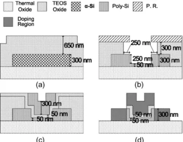
Fig. 1. (a)–(d) Schematic cross sections of the major fabrication steps of the proposed n-channel D-SAGRSD TFT.
and the gate masking misalignment error of the SARSD TFT would cause the unsymmetrical thicker channel region near the source/drain regions. Therefore, self-aligned gate RSD TFT would be preferred.
In this letter, a novel four-mask-step self-aligned gate RSD poly-Si TFT structure formed by the damascene process (D-SAGRSD TFT) is proposed. The new device features a thin active channel region and a thick source/drain region. The gate and RSD regions are self-aligned, and no additional mask is needed.
II. DEVICEFABRICATION
Fig. 1 shows the process flow of the D-SAGRSD TFT structure. First, a 300-nm α-Si layer for active region was de-posited by a low-pressure chemical vapor deposition (LPCVD) system using SiH4 at 550 ◦C on 500-nm thermal oxidized
silicon wafers. After patterning, the active region was formed using reactive ion etching (RIE) at this mask step. Then, the first (650-nm) plasma-enhanced chemical vapor deposition (PECVD) tetraethoxysilane (TEOS) oxide layer was deposited at 350◦C. Chemical–mechanical polishing (CMP) process was employed to planarize the first TEOS oxide surface, as shown in Fig. 1(a). The thickness of the first TEOS oxide above the active region after polishing is about 300 nm. After patterning, the RIE process was used to etch the α-Si layer, and then, selective
CHANG et al.: POLY-Si TFTs WITH A SELF-ALIGNED GATE AND RSD 807
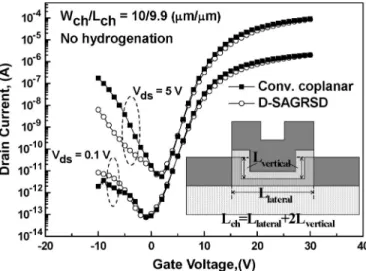
Fig. 2. Ids–Vgstransfer characteristics of the proposed D-SAGRSD TFT and
the conventional coplanar TFT. The insert plots are the cross-sectional views of the proposed D-SAGRSD TFT structure.
buffered oxide etching (BOE) was used to form a T-sharp gutter, as shown in Fig. 1(b). Because the α-Si layer had no stopper layer, the α-Si thin channel region thickness was controlled by etching rate (8.33 Å/s). Additionally, the α-Si film thickness was determined by an ellipsometer, and the thickness of the thin channel region was accurately controlled, with an error of within ±3% (50 ± 1.5 nm). After etching, the thickness of the active region became 50 nm. After the photoresist was removed, the α-Si film was annealed in nitrogen ambient at 600 ◦C for 24 h to become the poly-Si film. After recrys-tallization, the etching damages of the channel surface were recovered, and the surface roughness is approximately 3 nm. A 50-nm PECVD TEOS gate oxide layer was deposited at 350◦C, and then, a 300-nm LPCVD poly-Si film was deposited. After the CMP process was employed to planarize the poly-Si film surface to form the T-sharp gate, as shown in Fig. 1(c), the 50-nm TEOS gate oxide and the first TEOS oxide were removed by BOE solution. Then, gate, source, and drain regions were formed by ion implantation of phosphorous (dose = 5× 1015cm−2at 50 keV) and then activated in nitrogen ambient at 600◦C for 24 h, as shown in Fig. 1(d). After the source, drain, and gate activation, the second (500-nm) passivation TEOS oxide was deposited by PECVD. Contact holes were opened using wet etching of the passivation oxide layer. A layer of aluminum was then deposited by thermal coater system with a thickness of 600 nm. After metal patterning, a forming gas anneal is performed at 400◦C for 30 min. The total masks of our fabrication processes are four, which are less than those of the conventional processes in an RSD poly-Si TFT [8], [9]. For comparison, the conventional coplanar poly-Si TFTs with 50-nm channel thickness were also fabricated in the same run.
III. RESULTS ANDDISCUSSION
In Fig. 2, the Ids–Vgstransfer characteristics of the proposed
D-SAGRSD TFT structure compared with the conventional coplanar TFT were shown. It can be observed that, although the D-SAGRSD TFT has a slightly lowerON-state current and
a slightly higher minimum OFF-state current, a much lower
Fig. 3. Simulated lateral electric field distribution of the proposed D-SAGRSD TFT and the conventional coplanar TFT.
OFF-state leakage current (Vgs=−10 V and Vds= 5 V) can be
also obtained. The proposed TFT has two symmetrical thicker channel regions near the source and drain sides. These thicker channel regions have much more grain boundary traps than the thin channel region, and these grain boundary traps would cause the ON-state current to decrease and the minimum OFF-state current to increase. Moreover, the proposed TFT would have a higher threshold voltage and a larger subthreshold swing due to the bad channel control in the corners of the channel and the bad oxide/poly-Si interface of the vertical channel region. For theOFF-state current measured at higher drain and reverse gate biases (Vds= 5 V and Vgs=−10 V), the main reason of
a much lowerOFF-state current of the proposed D-SAGRSD is that the leakage current is determined by the electron–hole pair generation rate in the depletion region at the drain edge. The pair generation rate is strongly dependent on the number of trap states in the forbidden gap, lateral electric field, and generation volume of the depletion region [11]–[13]. Although a thicker drain region causes the generation volume of the D-SAGRSD TFT to increase, the maximum lateral electric field near the drain region of the D-SAGRSD TFT, as shown in Fig. 3, is also dropped from 1.11 to 1.00 MV/cm due to thick source/drain regions [10], [14]. At higher drain and reverse gate biases (Vds= 5 V and Vgs=−15 V), the leakage current would be
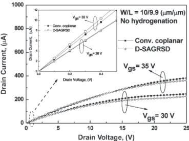
due to the thermionic field emission via grain boundary defects [15]. Although the generation volume would be increased, the D-SAGRSD TFT, therefore, would have a lower OFF-state leakage current than that of the conventional TFT because the maximum lateral electric field near the drain region is notably reduced. Fig. 4 shows the Ids–Vds curves of the proposed TFT
compared with the conventional TFT. In the insert plots, it can be observed that the proposed TFT has a lower source/drain parasitic resistance due to steeper slopes of Ids–Vds of the
proposed TFT in the linear region. However, in the saturation region, theON-state current of the proposed TFT is lower than that of the conventional TFT; it is because the maximum lateral electric field of the proposed TFT is also dropped due to thick source/drain regions.
808 IEEE ELECTRON DEVICE LETTERS, VOL. 28, NO. 9, SEPTEMBER 2007
Fig. 4. Ids–Vds output characteristics of the proposed D-SAGRSD TFT
and the conventional coplanar TFT. The insert plots are the Ids–Vds output
characteristics of the proposed D-SAGRSD TFT and the conventional coplanar TFT in the linear region.
IV. CONCLUSION
In this letter, a novel four-mask-step n-channel D-SAGRSD TFT was proposed and investigated. Remarkable OFF-state current can be obtained, and goodON/OFFcurrent ratio can be maintained for the proposed D-SAGRSD TFT. The self-aligned gate and raised source/drain regions can be formed without the additional mask step and therefore reduce the lateral electric field near the drain side to suppress theOFF-state current. This new TFT structure may be an attractive device structure for future high-performance large-area device applications.
REFERENCES
[1] I.-W. Wu, “Low temperature poly-Si TFT technology for AMLCD appli-cation,” in Proc. Tech. Dig. AMLCD, 1995, pp. 7–10.
[2] J. G. Fossum, A. Ortiz-Conde, H. Shichijo, and S. K. Banerjee, “Anom-alous leakage current in LPCVD polysilicon MOSFETs,” IEEE Trans.
Electron Devices, vol. ED-32, no. 9, pp. 1878–1884, Sep. 1985.
[3] J.-I. Han and C.-H. Kan, “A self-aligned offset polysilicon thin-film tran-sistor using photoresist reflow,” IEEE Electron Device Lett., vol. 20, no. 9, pp. 476–477, Sep. 1999.
[4] P.-S. Shih, C.-Y. Chang, T.-C. Chang, T.-Y. Huang, D.-Z. Peng, and C.-F. Yeh, “A novel lightly doped drain polysilicon thin-film transistor with oxide sidewall spacer formed by one-step selective liquid phase deposition,” IEEE Electron Device Lett., vol. 20, no. 8, pp. 421–423, Aug. 1999.
[5] T.-Y. Huang, I.-W. Wu, A. G. Lewis, A. Chiang, and R. H. Bruce, “Device sensitivity of field-plated high-voltage TFTs and their applica-tion to low-voltage operaapplica-tion,” IEEE Electron Device Lett., vol. 11, no. 11, pp. 541–543, Nov. 1990.
[6] K. Tanaka, K. Nakazawa, S. Suyama, and K. Kato, “Characteris-tics of field-induced-drain (FID) poly-Si TFTs with high on/off cur-rent,” IEEE Trans. Electron Devices, vol. ED-39, no. 4, pp. 916–920, Apr. 1992.
[7] K.-Y. Choi and M.-K. Han, “A novel gate-overlapped LDD poly-Si thin film transistor,” IEEE Electron Device Lett., vol. 17, no. 12, pp. 566–568, Dec. 1996.
[8] M. Yoshimi, M. Takahashi, T. Wada, K. Kato, S. Kambayashi, M. Kemmochi, and K. Natori, “Analysis of the drain breakdown mech-anism in ultra-thin-film SOI MOSFETs,” IEEE Trans. Electron Devices, vol. 37, no. 9, pp. 2015–2021, Sep. 1990.
[9] S. Zhang, C. Zhu, J. K. O. Sin, and P. K. T. Mok, “A novel ultrathin elevated channel low-temperature poly-Si TFT,” IEEE Electron Device
Lett., vol. 20, no. 11, pp. 569–571, Nov. 1999.
[10] K. M. Chang, G. M. Lin, C. G. Chen, and M. F. Hsieh, “A novel four-mask-step low-temperature polysilicon thin-film transistor with self-aligned raised source/drain (SARSD),” IEEE Electron Device Lett., vol. 28, no. 1, pp. 39–41, Jan. 2007.
[11] O. K. B. Lui, M. J. Quinn, S. W.-B. Tam, T. M. Brown, P. Migliorato, and H. Ohshima, “Investigation of the low field leakage current mechanism in polysilicon TFTs,” IEEE Trans. Electron Devices, vol. 45, no. 1, pp. 213–217, Jan. 1998.
[12] O. K. B. Lui and P. Migliorato, “A new generation-recombination model for device simulation including the Poole–Frenkel effect and phonon-assisted tunnelling,” Solid State Electron., vol. 41, no. 4, pp. 575–583, 1997.
[13] S. D. Brotherton, J. R. Ayres, and M. J. Trainor, “Control and analysis of leakage currents in poly-Si thin-film transistors,” J. Appl. Phys., vol. 79, no. 2, pp. 895–904, Jan. 1996.
[14] K. P. A. Kumar, J. K. O. Sin, C. T. Nguyen, and P. K. Ko, “Kink-free polycrystalline silicon double-gate elevated channel thin-film tran-sistors,” IEEE Trans. Electron Devices, vol. 45, no. 12, pp. 2514–2520, Dec. 1998.
[15] C. H. Kim and K.-S. Sohn, “Temperature dependent leakage currents in polycrystalline silicon thin film transistors,” J. Appl. Phys., vol. 81, no. 12, pp. 8084–8090, Jun. 1997.