Formation and nonvolatile memory effect of nickel-oxygen-silicon nanoparticles
Wei-Ren Chen, Ting-Chang Chang, Jui-Lung Yeh, Simon M. Sze, Chun-Yen Chang, and Uei-Shin Chen
Citation: Applied Physics Letters 91, 222105 (2007); doi: 10.1063/1.2816125 View online: http://dx.doi.org/10.1063/1.2816125
View Table of Contents: http://scitation.aip.org/content/aip/journal/apl/91/22?ver=pdfcov Published by the AIP Publishing
Articles you may be interested in
Nickel nanoparticle size and density effects on non-volatile memory performance J. Vac. Sci. Technol. B 31, 032204 (2013); 10.1116/1.4804407
Organic memory device with polyaniline nanoparticles embedded as charging elements Appl. Phys. Lett. 100, 163301 (2012); 10.1063/1.4704571
Oxygen vacancy mediated large magnetization in chemically synthesized Ni-doped HfO2 nanoparticle powder samples
J. Appl. Phys. 110, 063902 (2011); 10.1063/1.3634119
Nonvolatile memory characteristics of nickel-silicon-nitride nanocrystal Appl. Phys. Lett. 91, 082103 (2007); 10.1063/1.2760144
Optical properties and structure characterization of sapphire after Ni ion implantation and annealing J. Appl. Phys. 98, 073524 (2005); 10.1063/1.2084314
This article is copyrighted as indicated in the article. Reuse of AIP content is subject to the terms at: http://scitation.aip.org/termsconditions. Downloaded to IP: 140.113.38.11 On: Thu, 01 May 2014 00:03:26
Formation and nonvolatile memory effect of nickel-oxygen-silicon
nanoparticles
Wei-Ren Chen
Institute of Electronics, National Chiao Tung University, Hsin-Chu, Taiwan 300, Republic of China
Ting-Chang Changa兲
Department of Physics and Institute of Electro-Optical Engineering, Center for Nanoscience and Nanotechnology, National Sun Yat-set University, 70 Lien-hai Road, Kaohsiung 804, Taiwan
Jui-Lung Yeh, Simon M. Sze, and Chun-Yen Chang
Institute of Electronics, National Chiao Tung University, Hsin-Chu, Taiwan 300, Republic of China
Uei-Shin Chen
Department of Material Science and Engineering, National Tsing Hua University, Hsin-Chu, Taiwan 300, Republic of China
共Received 8 September 2007; accepted 1 November 2007; published online 27 November 2007兲 This study reveals the formation of nickel-oxygen-silicon nanoparticles with nonvolatile memory effect by sputtering a commixed target in argon and oxygen ambiance. A transmission electron microscope clearly shows the embedded nanoparticles in the silicon oxide and the constituent was examined by x-ray photoelectron spectroscopy. The capacitor structure with embedded nickel-oxygen-silicon nanoparticles was also studied and it exhibited hysteresis characteristics after electrical operation. The memory window and retention of nickel-oxygen-silicon nanoparticles were enough to apply on nonvolatile memory. In addition, a physical mechanism was deduced to expound the role of oxygen in the formation of nickel-oxygen-silicon nanoparticles. © 2007 American
Institute of Physics. 关DOI:10.1063/1.2816125兴
Nonvolatile memory 共NVM兲 plays an important role in the market of portable electronic products and is required for further possessing the high memory capacity, low-voltage, and high-speed operation for next-generation memory with scaling down devices.1–3However, the carriers will run out of the floating gate since the tunnel oxide of conventional NVM generates leakage paths during endurance test. There-fore, the tunnel oxide thickness is difficult to scale down in terms of charge retention and endurance characteristics. The nonvolatile nanoparticle memory devices are promising to substitute for the conventional floating gate memory because the discrete traps as the charge storage media have been re-ported that they can effectively avoid data loss under reliabil-ity test for the scaling down devices.4,5Among various nano-particles for memory technology, the metallic nanonano-particles were extensively investigated over semiconductor nanopar-ticles because of several benefits, such as enhanced gate con-trol ability共i.e., stronger coupling with the conduction chan-nel兲, higher density of states, and smaller energy disturbance and larger work function共faster programing time and better data retention兲.5,6In addition to the nanoparticle application, the induction of charge trapping layer can increase trap states to improve charge storage capacity for the metal nanoparticle memory devices, such as those embedded in the SiOx and
SiNxlayer.
7
In this work, a simple process was proposed to form nickel-oxygen-silicon共NiOSi兲 nanoparticles by sputter-ing a commixed target共Ni0.3Si0.7兲 in argon 共Ar兲/oxygen 共O2兲 ambiance at room temperature. Material and electrical analy-ses were performed to study the metal nanoparticles memory. This nonvolatile memory-cell structure in this letter was fabricated on a 4 in. p-type silicon共100兲 wafer. After a Radio Corporation of America共RCA兲 standard clean process which
removed native oxide and microparticles form wafer surface, 3-nm-thick tunnel oxide was thermally grown by a dry oxi-dation process at 950 ° C in an atmospheric pressure chemi-cal vapor deposition furnace. Afterwards, a 10-nm-thick charge tapping layer was deposited by reactive sputtering 共metallic mode兲 with the 4 in. Ni0.3Si0.7commixed target in
the Ar/O2 关24/2 SCCM 共SCCM denotes cubic centimeter per minute at STP兲兴 ambiance at room temperature. The di-rect current 共dc兲 sputtering power and pressure of sputter system were set to 80 W共the deposition rate ⬃0.2 Å/s兲 and 7 mtorr. During the foregoing process, nanoparticles could be found to precipitate and embed in SiOx layer because of
the competition of oxygen between silicon and nickel in the oxygen incorporated Ni0.3Si0.7layer共we discuss this
forma-tion mechanism of nanoparticles later兲. Then, a 30-nm-thick blocking oxide was deposited by the plasma enhanced chemical vapor deposition system at 300 ° C. Al gate elec-trodes were finally deposited and patterned to form a metal/ oxide/insulator/oxide/silicon 共MOIOS兲 structure. Transmis-sion electron microscope 共TEM兲 analysis and x-ray photoelectron spectroscopy共XPS兲 were adopted for micro-structure and chemical material analysis of nanoparticles. Electrical characteristics of the capacitance-voltage 共C-V兲 hysteresis were also measured by HP4284 Precision LCR Meter with high frequency 100 kHz. Moreover, we fabri-cated an oxygen deficient Ni0.3Si0.7layer which only used Ar
共24 SCCM兲 during sputter process as charge trapping layer of MOIOS structure 共control sample兲 to compare with the above-mentioned MOIOS structure for electrical characteris-tics of C-V.
Figure1共a兲shows a cross-sectional TEM image of con-trol sample. It was found that a uniform Ni0.3Si0.7layer was
deposited on the tunnel oxide and the thickness of the Ni0.3Si0.7 layer was about 10– 11 nm. However, the
cross-a兲Electronic mail: [email protected]
APPLIED PHYSICS LETTERS 91, 222105共2007兲
0003-6951/2007/91共22兲/222105/3/$23.00 91, 222105-1 © 2007 American Institute of Physics
This article is copyrighted as indicated in the article. Reuse of AIP content is subject to the terms at: http://scitation.aip.org/termsconditions. Downloaded to IP: 140.113.38.11 On: Thu, 01 May 2014 00:03:26
sectional TEM image of MOIOS structure containing spheri-cal and separated nanoparticles was shown in Fig.1共b兲. It is found that the thickness of tunnel oxide is larger than 3 nm by TEM analysis, since this redundant SiOxmatrix is formed
form oxygen incorporated Ni0.3Si0.7layer during sputter pro-cess. From TEM analysis, the average diameter of the nano-particles is approximately 5 – 6 nm and the area density of the nanoparticles is estimated to be about 1.33⫻1012cm−2.
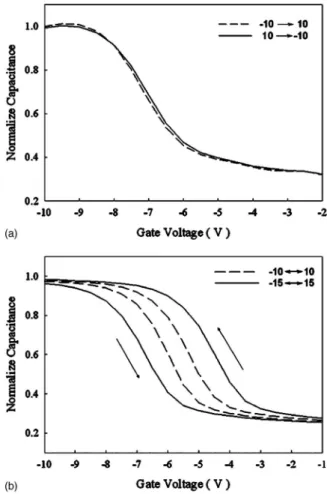
共C-V兲 hysteresis is shown in Figs.2共a兲and2共b兲 for the control sample and nanoparticles, respectively. From Fig.2共a兲, memory effect is not found in the control sample under ±10 V gate voltage operation. On the contrary, it is clearly observed that 0.8 and 2.5 V of memory windows can be obtained, respectively, under ±10 and ±15 V gate voltage operation for the MOIOS structure with nanoparticles, as shown in Fig.2共b兲. Hence, it is considered that the memory effect of nanoparticles is dominated by formation of nano-particles as compared with Fig.2共a兲. Moreover, the hyster-esis loops follow the counterclockwise direction due to in-jection of electrons from the inversion state and discharge of electrons from the accumulation state of Si substrate. The memory window of MOIOS with nanoparticles is enough to determine data information by different memory window for nonvolatile memory application. As a result, our electrical characteristics of C-V show that formation and nonvolatile memory effect of nanoparticles are influenced by oxygen doping during sputter process.
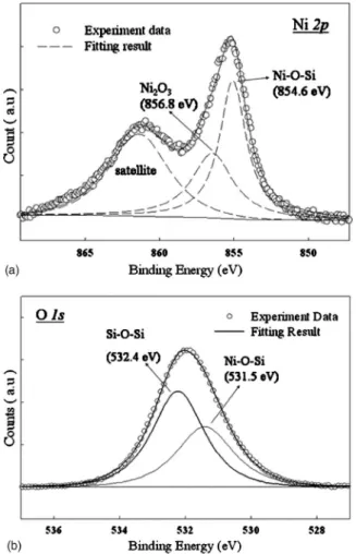
In our work, the chemical composition of the nanopar-ticles is demonstrated by XPS analysis using an Al K␣共1486.6 eV兲 x-ray radiation, as shown in Fig. 3. Figure3共a兲exhibits the XPS Ni 2p core-level photoemission spectra that consist of two main peaks, Ni 2p3/2and satellite. According to previous research,8,9 the composition of Ni
2p3/2 peak can be separated out Ni– O – Si共854.6 eV兲 and
Ni2O3共856.8 eV兲 by fitting results of XPS analysis.10 The nanoparticle is thereby believed to be composed of Ni–O–Si ternary element. Moreover, the XPS O 1s photoemission spectra can be utilized to verify this contention, as shown in Fig.3共b兲. By fitting result of experiment data, it is found that the main peak can be composed into two components which center at 531.5 and 532.4 eV corresponding to Ni–O–Si bond and Si–O–Si bond, respectively.9 In addition, we can use XPS analysis to evaluate the atomic concentration in the trapping layer, which is 14%, 47%, and 39% for nickel, sili-con, and oxygen of charge trapping layer, respectively.
For the formation of Ni–O–Si nanoparticles during sput-ter process, the enthalpies共−⌬H兲 of Si–O, Ni–O and Ni–Si at room temperature are 799, 382, and 318 kJ mol−1, respectively.11Because of the higher enthalpy of Si–O com-pared with Ni–O, the oxygen radicals can interact with Si atom easier than with Ni atom on the wafer surface during the sputter process. It can be explained that an internal oxi-dation reaction will induce self-assembled phenomenon of Ni–O–Si nanoparticles, which is dependent on the different enthalpies of compounds of charge trapping layer, as shown in Fig.2共b兲. Therefore, Ni–O–Si nanoparticles can be formed at low temperature and no need of further thermal annealing in our experimental method.
Figure 4共a兲 demonstrates the data retention characteris-tics of the nonvolatile NiOSi nanoparticles memory at room temperature. The memory cell is programed by 10 V for 5 s, and erased −10 V for 5 s. The flatband voltage shift is
ob-FIG. 1. Cross-sectional transmission electron microscope共TEM兲 analysis of 共a兲 control sample, and 共b兲 MOIOS structure containing nanoparticles. The nanoparticles size and density are about 5 – 6 nm and 1.33⫻1012cm−2, re-spectively. The inset shows sketch diagrams of control sample and MOIOS structure.
FIG. 2. Capacitance-voltage共C-V兲 hystereses of MOIOS structure with 共a兲 the control sample, and共b兲 NiOSi nanoparticles. The memory windows of NiOSi nanoparticles 0.8 and 2.5 V can be obtained under ±10共dash line兲 and ±15 V共solid line兲 gate voltage operation, respectively.
222105-2 Chen et al. Appl. Phys. Lett. 91, 222105共2007兲
This article is copyrighted as indicated in the article. Reuse of AIP content is subject to the terms at: http://scitation.aip.org/termsconditions. Downloaded to IP: 140.113.38.11 On: Thu, 01 May 2014 00:03:26
tained by comparing the C-V curves from a charged state and the quasineutral state. The memory window significantly de-cays during the first 100 s due to charge emission from the shallow traps in SiOx matrix to the substrate. However, a
1.4 V memory window共charge remained ratio of 50%兲 can be obtained even after 10 yr by analyzing the extrapolation value of retention data共stable range of 102– 4⫻104s兲.
Figure4共b兲shows the programing/erasing characteristics of NiOSi nanoparticles under ±10 and ±15 V. The flatband voltage shift is increased as the programing/erasing voltage increased at the same programing/erasing duration, and also increased with the increasing programing/erasing duration at the same programing/erasing voltage. Moreover, the defined window 0.5 V can be obtained at programing/erasing ⬃10−4 s under ±10 V operation. This memory device reveals
a high speed programing/erasing time for further nonvolatile memory application.
In conclusion, the NiOSi nanoparticles embedded in the SiOxlayer were fabricated for the nonvolatile memory
appli-cation by sputtering a commixed target in an Ar/O2
environ-ment at room temperature. Due to different enthalpies of Si–O, Ni–O, and Ni–Si, the nanoparticles can be self-assembly fabrication in this study. A larger memory window of 2.5 V was clearly observed after ±15 V voltage sweep and the retention can get up to 10 yr for NVM application. In addition, this memory device is suitable for high speed op-eration and the fabrication technique of NiOSi nanoparticles can be compatible with current manufacture process of the integrated circuit manufacture.
This work was performed at National Nano Device Laboratory and was supported by the National Science Council of the Republic of China under Contract Nos. NSC 96-2221-E-009-202-MY3, NSC 96-2112-M-110-013, NSC 96-2120-M-110-001, and NSC 95-2221-E-009-316-MY2. Furthermore, this work was partially supported by MOEA Technology Development for Academia Project No. 94-EC-17-A-07-S1-046 and MOE ATU Program “Aim for the Top University” No. 95W803.
1R. Bez, E. Camerlenghi, A. Modelli, and A. Visconti, Proc. IEEE 91, 4 共2003兲.
2J. D. Blauwe, IEEE Trans. Nanotechnol. 1, 72共2002兲.
3C. Y. Lu, T. C. Lu, and R. Liu, Proceedings of 13th IPFA, 2006 共unpublished兲.
4S. Tiwari, F. Rana, K. Chan, H. Hanafi, W. Chan, and D. Buchanan, Tech. Dig. - Int. Electron Devices Meet. 521共1995兲.
5Z. Liu, C. Lee, V. Narayanan, G. Pei, and E. C. Kan, IEEE Trans. Electron Devices 49, 9共2002兲.
6S. K. Samanta, W. J. Yoo, G. Samudra, E. S. Tok, L. K. Bera, and N. Balasubramanian, Appl. Phys. Lett. 87, 113110共2005兲.
7C. Busseret, A. Souifi, T. Baron, S. Monfray, N. Buffet, E. Gautier, and M. N. Semeria, Mater. Sci. Eng., C 19, 237共2002兲.
8R. Zhao, Y. H. Lin, X. Zhou, M. Li, and C. W. Nan, J. Appl. Phys. 100, 046102共2006兲.
9A. A. Galuska, J. Vac. Sci. Technol. A 9, 2907共1991兲.
10C. D. Wagner, J. F. Moulder, L. E. Davis, and W. M. Riggs, Handbook of
X-ray photoelectron spectroscopy 共Perkin-Elmer, Eden Prairie, MN,
1995兲, p. 85.
11D. R. Lide, CRC Handbook of Chemistry and Physics, 81st ed.共CRC, Boca Raton, FL, 2000兲, Vol. 81, pp. 3–5.
FIG. 3. 共a兲 Ni 2p and 共b兲 O 1 s x-ray photoelectron spectroscopy 共XPS兲 analysis of the charge trapping layer. Empty circles and straight line indicate experimental and fitting results, respectively.
FIG. 4. 共a兲 Retention characteristics of the memory structure with NiOSi nanoparticles using a ±10 V gate voltage stress for 5 s at room temperature. The dotted line is the extrapolated value of retention data after 100 s.共b兲 Programing and erasing characteristics of the NiOSi nanoparticles under ±10 and ±15 V gate voltage.
222105-3 Chen et al. Appl. Phys. Lett. 91, 222105共2007兲
This article is copyrighted as indicated in the article. Reuse of AIP content is subject to the terms at: http://scitation.aip.org/termsconditions. Downloaded to IP: 140.113.38.11 On: Thu, 01 May 2014 00:03:26