Effect of Zr
ÕTi Ratios on Characterization of Pb„Zr
xTi
1Àx…O
3Thin Films on Al
2O
3Buffered Si for One-Transistor
Memory Applications
Chia-Liang Sun,a,zJung-Jui Hsu,aSan-Yuan Chen,aand Albert Chinb aDepartment of Materials Science and Engineering, and
bDepartment of Electronics Engineering, National Chiao Tung University, Hsinchu, Taiwan
Pb(ZrxTi1⫺x)O3共PZT兲 thin films have been prepared on Al2O3/Si and PbTiO3/Al2O3/Si substrates, respectively. On Al2O3/Si substrates, Ti-rich PZT thin films had lower perovskite transformation temperatures than those of Zr-rich PZT films. Therefore, PbTiO3 was used as the seeding layer on Al2O3/Si to form a PbTiO3/Al2O3/Si substrate. The threshold voltage shift of a PZT(53/47)/PbTiO3/Al2O3/Si capacitor reaches 9 V with⫾10 V writing voltages, which is much larger than the 2 V of the PZT(0/100)/PbTiO3/Al2O3/Si capacitor. Different memory mechanisms in the capacitance-voltage characteristics of capacitors were further examined and discussed in this paper.
© 2003 The Electrochemical Society. 关DOI: 10.1149/1.1542901兴 All rights reserved.
Manuscript submitted March 4, 2002; revised manuscript received August 28, 2002. Available electronically January 28, 2003.
Recently, one-transistor memory has attracted much attention be-cause of the excellent performance.1-4Unfortunately, little progress has been achieved in one-transistor memory because it is difficult to integrate different materials as stack gate dielectrics and to fabricate a metal/ferroelectric/insulator/Si 共MFIS兲 capacitor structure.5,6 Al-though the effects of different substrates and annealing temperatures have been studied,7,8the ferroelectric material in each research has the same composition, and the related influences were not discussed as in the study in a metal/ferroelectric/metal capacitor.9Thus, it is necessary to do some systematic research on the effects of ferroelec-tric material compositions on the memory properties in the MFIS capacitor.
The solid solution Pb(ZrxTi1⫺x)O3共PZT兲 system has a complex
phase diagram containing materials exhibiting unique properties such as piezoelectricity, pyroelectricity, and ferroelectricity.10 All these properties are strongly related to the different structures and compositions in the PZT solid solution. For example, it is well known that the coupling factor and permittivity of PZT located at the morphotropic phase boundary共MPB兲 show maximum values.11 Among its many superior properties, the high dielectric constant and remnant polarization of PZT have made it a promising material for memory applications.12,13It is necessary to study the effect of com-positions on the memory properties of an MFIS capacitor with PZT as the ferroelectric layer. In this paper, we have prepared PZT thin films on Al2O3/Si substrates as the MFIS capacitor and investigated
the characteristics related to four Zr/Ti ratios共0/100, 30/70, 53/47, and 60/40兲 to find the relationship between the electrical properties of an MFIS capacitor and the phase and microstructure of PZT films with different compositions.
Experimental
PZT stock solution synthesis and thin-film deposition.—PZT ferroelectric thin films were deposited by the chemical solution deposition method using multiple spin coating. The advantage of chemical solution deposition was the accuracy of composition con-trol. For chemical solution synthesis, lead acetate trihydrate, zirco-nium n-propoxide, and titazirco-nium isopropoxide were used as precur-sors and dissolved in the solvents composed of acetic acid and methanol in sequence.7An excess lead precursor was added to com-pensate the lead loss during crystallization, and four Zr/Ti ratios of the chemical solution were varied from titanium-rich共Ti-rich兲 com-positions (Zr/Ti⫽ 0/100 and 30/70兲 to zirconium-rich 共Zr-rich兲 compositions (Zr/Ti⫽ 53/47 and 60/40兲. After each coating, the
zE-mail: [email protected]
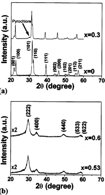
Figure 1. XRD patterns of Pb(ZrxTi1⫺x)O3thin films with共a兲 x ⫽ 0 and 0.3 and共b兲 x ⫽ 0.53 and x ⫽ 0.6 on Al2O3/Si.
Journal of The Electrochemical Society, 150共3兲 G187-G191 共2003兲 0013-4651/2003/150共3兲/G187/5/$7.00 © The Electrochemical Society, Inc.
wet films were pyrolyzed for several minutes, and the multilayer films, 650 nm thick, were annealed at 650°C for 1 h.
Preparation of Al2O3/Si and PbTiO3( PTO)/Al2O3/Si
substrates.—To fabricate the insulator buffered layer, a 10 nm thick Al2O3gate dielectric was formed on p-type共100兲 Si wafers
follow-ing our previously reported procedure.14,15For preparing the seeding layer, 80 nm thick lead titanate 共PTO兲 film was deposited on Al2O3/Si and then annealed at 550°C so that the PTO/Al2O3/Si
substrates could be obtained.
Film and capacitor characterization.—We have used X-ray dif-fraction共XRD兲 to determine the phase and the crystallinity of PZT. The surface morphology and the thickness of PZT were observed by scanning electron microscopy 共SEM兲. For electrical measurement, Au was used as the upper electrode with an area of 5
⫻ 10⫺4 cm2
, and the Al bottom electrode was deposited at the back side. Capacitance-voltage 共C-V兲 and current density-voltage 共J-V兲 characteristics were measured to check the electrical properties of PZT capacitors.
Figure 2. XRD patterns of Pb(ZrxTi1⫺x)O3thin films with共a兲 x ⫽ 0 and 0.3 and共b兲 x ⫽ 0.53 and x ⫽ 0.6 on PbTiO3/Al2O3/Si.
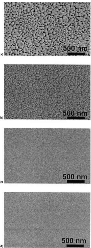
Figure 3. SEM images of Pb(ZrxTi1⫺x)O3thin films with共a兲 x ⫽ 0, 共b兲 x ⫽ 0.3, 共c兲 x ⫽ 0.53, and 共d兲 x ⫽ 0.6 on PbTiO3/Al2O3/Si.
Results and Discussion
Figures 1a and b show the XRD patterns of Pb(ZrxTi1⫺x)O3
deposited on Al2O3(10 nm)/Si, with x⫽ 0-0.3 and 0.5-0.6,
respec-tively. As shown in Fig. 1a, the major phase of Ti-rich PZT films is a perovskite phase, although a small and broad peak at diffraction angle 2 ⬃ 29.5° belonging to a pyrochlore phase is observed for the PZT共30/70兲. In contrast, the XRD patterns in Fig. 1b show that Zr-rich PZT films have a nonferroelectric pyrochlore phase rather than a perovskite phase. Therefore, it is suggested that PZT films with higher Zr/Ti ratios have higher perovskite transformation tem-peratures. Although this tendency is similar to that published in the literature,16 the transformation temperatures of PZT on Al2O3/Si
substrates are obviously higher than those on single-crystal sapphire substrates.16This phenomenon may occur because the nucleation of perovskite PZT would be easier on crystalline substrates than on amorphous substrates.17
To reduce the perovskite transformation temperature of PZT, an additional PTO seeding layer was deposited on Al2O3/Si substrates
prior to the PZT films. Figure 2 shows the XRD patterns of PZT thin films deposited on PTO/Al2O3/Si substrates with a seeding layer. In
Fig. 2b, clearly, the formation of the pyrochlore phase is inhibited. Therefore, the PTO seeding layer is proved able to lower the trans-formation temperatures, which is similar to the result on crystalline substrates.16,18 However, the intensity and full width at half-maximum共fwhm兲 of the major XRD peak position of Zr-rich PZT
共x 0.53 and 0.60兲 at 31.5° are lower and larger than that on Pt
substrates, respectively.8These results imply that the microstructure of Zr-rich PZT films may be different from that on Pt substrates.
We have further used SEM to observe the microstructure of PZT thin films on PTO/Al2O3/Si substrates. Figure 3a-d display the
sur-face morphology of Pb(ZrxTi1⫺x)O3 films on PTO/Al2O3/Si
sub-strates, with x⫽ 0, 0.3, 0.53, and 0.60, respectively. The micro-structures for Ti-rich PZT show a large grain size, greater than 50 nm. In contrast, the microstructures for Zr-rich PZT exhibit a very small grain size, much less than 50 nm. These results are consistent with the weak XRD intensity and large fwhm shown in Fig. 1. These SEM images indicate that inserting the additional PT seeding layer could greatly suppress the nucleation of the pyrochlore phase, but a higher process temperature is still required for Zr-rich PZT with a perovskite phase to improve the crystallinity.
We have studied the memory property of PZT on PTO/Al2O3/Si
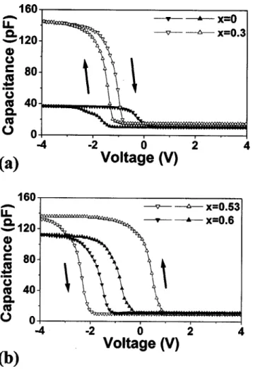
substrates using C-V measurements at 1 MHz. Figure 4a, b show the C-V characteristics of PZT/PTO/Al2O3/Si capacitors. Under the
same⫾5 V sweep voltages, the Ti-rich PZT capacitors (x ⫽ 0 and 0.3兲 show a clockwise hysteresis loop, but the Zr-rich PZT capaci-tors show a counterclockwise loop. It is believed that the clockwise hysteresis loop is due to the ferroelectricity, while the counterclock-wise loop is the result of a charge trapping effect.4Although both
Figure 4. C-V characteristics of Pb(ZrxTi1⫺x)O3/PbTiO3/Al2O3/Si capaci-tors with共a兲 x ⫽ 0 and 0.3 and 共b兲 x ⫽ 0.53 and 0.6 under ⫾5 V sweep voltage.
Figure 5. Memory window of Pb(ZrxTi1⫺x)O3/PbTiO3/Al2O3/Si capaci-tors with共a兲 x ⫽ 0 and 0.3 and 共b兲 x ⫽ 0.53 and 0.6.
effects can be used for memory devices, the observed ferroelectric hysteresis loop may be due to a better ferroelectric material quality than that in the charge trapping case. These results are again consis-tent with the XRD and SEM results shown previously. However, the strong dependence of ferroelectric property on composition seems to be independent of the Al2O3 dielectric process, suggesting the
ex-cellent quality of the Al2O3 gate dielectric14,15 as compared with
low temperature deposited silicon nitride.
We have also measured the memory window of PZT/PTO/Al2O3/Si capacitors at different program/erase voltages.
Figure 5a, b summarize the measured threshold voltage shift (⌬VT)
for Ti-rich and Zr-rich PZT/PTO/Al2O3/Si capacitors, respectively.
A positive threshold voltage shift is attributed to the ferroelectric effect, while a negative threshold shift is due to the charge trapping effect. Note that the threshold voltage shift of Ti-rich PZT capacitors changes from positive to negative as increasing bias voltage, which may be due to the increasing leakage current and charge trapping at high voltages. A memory window of 1.7 V is measured for PZT共0/ 100兲 capacitors at ⫾5 V bias voltage, indicating a good material quality for Ti-rich PZT formed at 650°C. Besides, the larger memory window at x⫽ 0 may be due to the smaller dielectric constant共k兲 that may cause a larger electric field drop in PZT than that in the Al2O3dielectric.8Additionally, other reasons may be the
larger grain size of Ti-rich PZT and that it has the same tetragonal unit cell as that of the bottom seeding layer. In contrast, only a negative threshold voltage shift is found for Zr-rich PZT capacitors. However, a similar trend of increasing memory window with in-creasing write voltages also occurs in this case, which depicts that the charge injection dominates the memory effect at high voltages regardless of the different composition of PZT capacitors.
We have summarized the composition dependence of PZT on threshold voltage shift, and the result is shown in Fig. 6. The hori-zontal axis from 0 to 1 represents the gradual composition change from PZT共0/100兲 to PZT共100/0兲. The similar trend of the larger threshold voltage shift with increasing write voltage is observed for all PZT capacitors due to the charge trapping contribution. However, from the memory device point of view, a desired large memory window is the key factor regardless of the effect from either the ferroelectric or charge trapping mechanism. Therefore, the PZT ca-pacitors with composition close to that of the MPB would be the most suitable ferroelectric material for memory application, and a memory window as large as 9 V is obtained.
We have also measured the J-V characteristics to further study the memory characteristics. Figure 7a, b show the J-V characteristics
of Ti-rich and Zr-rich PZT capacitors, respectively. No breakdown phenomenon occurs in the high voltage region up to⫺20 V for all four PZT capacitors, indicating that Al2O3would be a suitable
in-sulator material. The leakage current of PZT capacitor with x⫽ 0 is 2.2⫻ 10⫺6A/cm2at⫺5 V, which is lower than that of other PZT capacitors. This result suggests that the difference in crystal systems between PZT films and the seeding layer may induce some interface traps that increase the leakage current.
Table I summarizes the characteristics of PZT capacitors with different Zr/Ti ratios. By the addition of a seeding layer on amor-phous Al2O3substrates, the transformation temperature are reduced.
Furthermore, the relatively lower k is desirable for Ti-rich PZT in a stacked gate dielectric because a larger electric field will drop on PZT, giving a larger memory window.
Conclusions
We have compared the characteristics of PZT with different com-positions on Al2O3/Si and PTO/Al2O3/Si substrates. A PTO
seed-ing layer can lower the perovskite transformation temperatures and help the nucleation of the perovskite phase. However, Zr-rich PZT films on PTO/Al2O3/Si substrates have dielectric constants that are
lower than expected values due to the small grain size. In
compari-Figure 6. Threshold voltage shift of Pb(ZrxTi1⫺x)O3/PbTiO3/Al2O3/Si ca-pacitors under different sweep voltages.
Figure 7. J-V characteristics of Pb(ZrxTi1⫺x)O3/PbTiO3/Al2O3/Si with共a兲 x⫽ 0 and 0.3 and 共b兲 x ⫽ 0.53 and 0.6.
son with Zr-rich PZT/PTO/Al2O3/Si capacitors, the memory
prop-erties of Ti-rich PZT/PTO/Al2O3/Si capacitors are ferroelectric C-V
hysteresis loops, and the lower leakage current is due to the lower dielectric constant of Ti-rich PZT and the same crystal system of Ti-rich PZT and PTO.
Acknowledgments
This work has been supported by the National Science Council contract NSC91-2215-E009-051 of Taiwan.
National Chiao Tung University assisted in meeting the publication costs of this article.
References
1. S. Y. Wu, J. Appl. Phys., 50, 4314共1979兲.
2. S. L. Miller and P. J. MacWhorter, J. Appl. Phys., 72, 5999共1992兲.
3. A. Chin, M. Y. Yang, C. L. Sun, and S. Y. Chen, IEEE Electron Device Lett., 22, 336共2001兲.
4. M. Y. Yang, S. B. Chen, A. Chin, C. L. Sun, B. C. Lan, and S. Y. Chen, Tech. Dig. Int. Electron Devices Meet., 2001, 36គ 03.1.
5. K. Sugibuchi, Y. Kurogi, and N. Endo, J. Appl. Phys., 46, 2877共1975兲. 6. N. Maffei and S. B. Krupanidhi, J. Appl. Phys., 72, 3617共1992兲.
7. C. L. Sun, S. Y. Chen, M. Y. Yang, and A. Chin, J. Electrochem. Soc., 148, F203 共2001兲.
8. C. L. Sun, S. Y. Chen, S. B. Chen, and A. Chin, Appl. Phys. Lett., 80, 1984共2002兲. 9. W. Zhu, Z. Q. Liu, W. Lu, M. S. Tse, H. S. Tan, and X. Yao, J. Appl. Phys., 79,
4283共1996兲.
10. A. J. Moulson and J. M. Herbert, Electroceramics, Chapman & Hall Press, London, 265共1990兲.
11. M. Klee, R. Eusemann, R. Waser, W. Brand, and H. V. Hal, J. Appl. Phys., 72, 1566 共1992兲.
12. S. Kobayashi, K. Amanuma, H. Mori, N. Kasai, Y. Maejima, A. Seike, N. Tanabe, T. Tatsumi, J. Yamada, T. Miwa, H. Koike, H. Hada, and H. Toyoshima, Tech. Dig. Int. Electron Devices Meet., 2000, 783.
13. D. Jung, H. Kim, Y. Song, N. Jang, B. Koo, S. Lee, S. Park, Y. Park, and K. Kim, Tech. Dig. Int. Electron Devices Meet., 2000, 801.
14. A. Chin, Y. H. Wu, S. B. Chen, C. C. Liao, W. J. Chen, Symposium on VLSI Technology, IEEE, p. 16共2000兲.
15. A. Chin, C. C. Liao, C. H. Lu, W. J. Chen, and C. Tsai, Symposium on VLSI Technology, IEEE, p. 135共1999兲.
16. C. K. Kwok and S. B. Desu, J. Mater. Res., 8, 339共1993兲. 17. N. Floquet, J. Hector, and P. Gaucher, J. Appl. Phys., 84, 3815共1998兲. 18. Y. Liu, C. N. Wu, and T. Watanabe, J. Mater. Sci., 34, 4129共1999兲.
Table I. Characteristics of Pb„ZrxTi1Àx…O3ÕPbTiO3ÕAl2ÕO3ÕSi
capacitors. x ⌬V T共V兲 at⫾5 V ⌬V T共V兲 at⫾10 V k of stacked PZT films Capacitance 共pF兲 of gate dielectrics Leakage current density at 165 kV/cm 共A/cm2兲 0 1.49 0.91 56.03 37 6.24⫻ 10⫺6 0.3 0.40 ⫺1.50 336.89 146 6.12⫻ 10⫺6 0.53 ⫺2.83 ⫺8.94 303.03 137 9.86⫻ 10⫺6 0.6 ⫺0.78 ⫺5.83 225.06 113 2.20⫻ 10⫺6