DUAL-WIDEBAND BANDPASS FILTERS WITH EX-TENDED STOPBAND BASED ON COUPLED-LINE AND COUPLED THREE-LINE RESONATORS
J.-T. Kuo1, *, C.-Y. Fan2, and S.-C. Tang3
1Department of Electronic Engineering, Chang Gung University,
Taoyuan, Taiwan
2Mediatek Corp., Hsinchu, Taiwan
3Institute of Communication Engineering, National Chiao Tung
University, Hsinchu, Taiwan
Abstract—Coupled-line and coupled three-line resonators are pro-posed to design dual-wideband bandpass filters. Compared with the shorted and open stubs shunt at the same locations of the main line, in addition to saving the circuit area, these resonators provide alter-native ways to the design of dual-wideband filters, with larger possible bandwidths and different frequency ratio of the two center passbands. The geometric parameters of the coupled-line and the coupled three-line structures are determined by deriving their equivalent circuits to a shunt open stub in parallel connection with a shunt shorted stub. To extend the upper stopband, a cross-shaped admittance inverter is devised to play the role of the 90-degree transmission line section at the center frequency and to create transmission zeros at the spurious passbands, so that the upper stopband of the filter can be extended. It is a quarter-wave section with two open stubs of unequal lengths shunt at its center. For demonstration, two dual-wideband bandpass filters operating at 900/1575 MHz and 900/2000 MHz are fabricated and measured. Measured results of the experimental circuits show good agreement with simulated responses.
1. INTRODUCTION
Bandpass filters are one of the key components in the RF front end of a microwave communication system. Design of single-band bandpass
Received 1 December 2011, Accepted 26 December 2011, Scheduled 9 January 2012 * Corresponding author: Jen-Tsai Kuo ([email protected]).
filters has been well documented in, e.g., [1]. Rapid advance of the modern wireless communication systems has created demands of multi-band active and passive microwave/RF devices. Design of dual-multi-band filters at microwave frequencies is still challenging since it has to take into consideration many parameters, including center frequency, bandwidth, and/or passband functions at the two passbands There have been many innovative dual-band bandpass filter designs [2–8]. In [2], compact miniaturized hairpin resonators are utilized in a 2 × 2 configuration to design two quasi-elliptic function passbands. Stepped-impedance resonator (SIR) is a versatile multi-resonance element suitable for multi-band purpose [3]. In [4], SIRs in parallel-coupled configuration are devised to synthesize a dual-band response. In [5], cascaded folded tri-section SIRs are used to design compact dual-band dual-bandpass filters. In [6], dual-band filter are built by open-loop ring resonators incorporating with the electric and magnetic coupling structures. In [7], a dual feeding structure embedded uniform impedance resonator is used to design a dual-band bandpass filter. In addition, stub-loaded resonators are an alternative technique for such designs since the two center frequencies can be easily controlled by tuning length of the stub [8, 9]. In [10], compact dual-band filters are developed based on the dual-resonance composite resonators by using integrated passive device technology on a glass substrate. The magnetic and electric mixed coupling in a high-density wiring transformer configuration generates multiple transmission zeros for enhancing passband isolation and stopband rejection. In [11], an extremely compact dual-band filter is designed with the meandered technology and fractal geometry. The skirt selectivity is attractive since two transmission zeros are created on both sides of the two passbands.
In [2, 4–11], the center frequencies of the two passbands can be flexibly tuned; however, the design methods are rather suitable for narrow-band filters. It is well known that a shunt shorted stub can provide a wideband bandpass response whereas a shunt open circuit stub filter creates a bandstop response with a relatively small bandwidth [1]. Therefore, along the main transmission line, a shorted and an open stub connected in shunt at the same point will produce a wide passband with a narrow-band bandstop characteristic in the middle, or equivalently a dual-wideband bandpass response with good passband isolation [12]. In [13], SIRs are used to substitute both the shunt open- and short-stubs in order to have different bandwidths for the two designated passbands.
Stopband extension has been an important issue in filter design recently. Ideal bandpass filters have an infinite upper stopband.
Many effective techniques have been proposed and incorporated with the filter synthesis to achieve a wide upper rejection band [14–18]. For the parallel-coupled filters, higher order unwanted passbands occur at the multiples of the fundamental frequency. Suspended substrate structure [14] and the corrugated coupled-line in [15] are good techniques to make the even- and odd-mode phase velocities identical so that the spurious passband at the second harmonic can be suppressed. In [16], multi-spurious suppression is achieved by generating transmission zeros with over-coupled stages and the stopband can be extended to the fifth harmonic of the design frequency. In [17], SIRs are applied to push higher order resonances to much higher frequencies. With appropriate input/output tapping structure, extra transmission zeros are created to suppress the leading two higher order harmonics. In [18], dual-band bandpass filters are implemented by parallel coupled SIRs. The stopband performance is greatly improved by tuning the coupled lengths and the positions of the input/output transformers, which can provide multi-spurious suppression. To date, it has still been quite challenging to design dual-band dual-bandpass filters equipped with a wide upper stopdual-band, so that only few publications [19] can be found in open literature.
In this paper, coupled-line and coupled three-line resonators are proposed for design of dual-band bandpass filters with relatively wide bandwidths. A cross-shaped admittance inverter is also devised to extend the upper stopband. The extension relies on the creation of transmission zeros at the spurious passbands. The cross-shaped inverter consists of a transmission line section shunt with two open stubs at its middle. The lengths of the stubs are determined by the designated zero frequencies. Analysis formulas for the proposed inverter will be derived. This paper is organized as follows. Secs. 2 and 3 describe the resonance characteristics of coupled-line and coupled
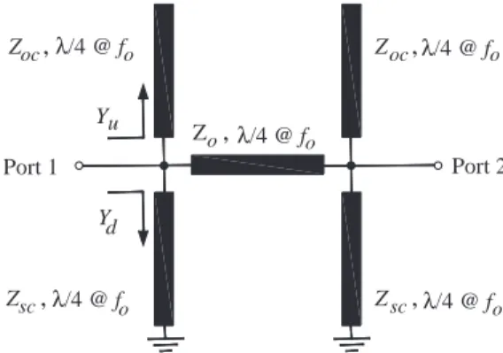
Port 1 Port 2 Yu Yd Zoc , o Zoc , λ/4 @ f o Zo , o Zsc , o Zsc , o λ/4 @ f λ/4 @ f λ/4 @ f λ/4 @ f
three-line resonators, respectively. Sec. 4 formulates the analysis of the proposed inverter for use to replace the conventional inverter and to create transmission zeros for multi-spurious suppression. Sec. 5 will compare the measured responses of two fabricated circuits with the simulation data, and Sec. 6 draws the conclusion.
2. CONVENTIONAL STRUCTURE AND COUPLED-LINE RESONATORS
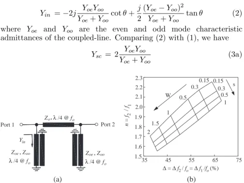
Figure 1 depicts a second-order dual-band bandpass filter with parallel open-circuit and shorted stubs [12, 13]. The shorted stubs will generate a wideband bandpass filter, and at its center frequency the open stubs will create a bandstop filter with a smaller bandwidth. Their bandwidths are determined by the stub characteristic impedances. Obviously, both the bandpass and the bandstop filters share the same center frequency, denoted as fo herein, since the Zoc and the Zsc stubs are commensurate. As a result, the circuit in Figure 1 possesses a dual-passband response with a rejection band in the middle. Let the center frequencies of the two passbands are f1and f2, respectively. It is
known that both the above bandpass and bandstop filter responses are symmetric about fo. Thus, the two bandwidths of the dual-passband
response will be identical.
1 1.5 2 0.5 0.3 0.15 2 o 1 o Ws 2 1.5 1 0.5 0.3 0.15 Wo 30 35 40 45 50 55 60 2.0 2.2 2.4 2.6 2.8 3.8 ∆ = ∆ f / f = ∆ f / f (%) n = f / f 2 1 3.6 3.4 3.2 3.0
Figure 2. Frequency ratio and bandwidth design graph for the dual-band dual-bandpass filter. Substrate: εr = 10.2, thickness d = 1.27 mm. Ws and Wo denote the line widths of the short-circuited stubs and open-circuit stubs, respectively.
By using the microstrip technology, when the widths of the open stubs (Wo) and the shorted stubs (Ws) are given, the frequency ratio
f2/f1 and bandwidth (∆ = ∆f1/fo = ∆f2/fo) design graph can be established as shown in Figure 2, for a substrate with εr = 10.2 and
thickness of 1.27 mm. It is known that best resolution for practical microstrip fabrication is about 0.15 mm. From Figure 2, it can be observed that the frequency ratio is always larger than 2, and the fractional bandwidth is less than 60%.
In Figure 1, the input admittance looking to the two shunt stubs
Yin can be written as
Yin= −jYsccot θ + jYoctan θ (1)
where Ysc = Z−1
sc and Yoc = Zoc−1. Figure 3(a) shows the use of the
coupled-line resonators. Obviously, the circuit area is reduced by around 50%, as compared with that in Figure 1. By treating the coupled-line as a four-port network, the 4 × 4 Y - or Z-matrix can be known [1]. By shorting two diagonal ports and open one of the two ports, the input admittance can be derived as
Yin = −2jYYoeYoo oe+ Yoocot θ + j 2 (Yoe− Yoo)2 Yoe+ Yoo tan θ (2)
where Yoe and Yoo are the even and odd mode characteristic
admittances of the coupled-line. Comparing (2) with (1), we have
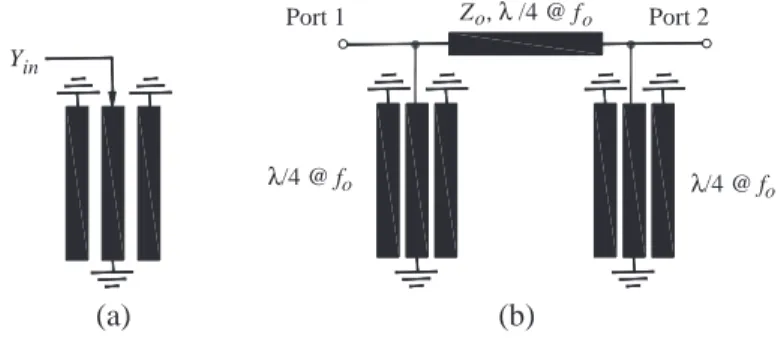
Ysc = 2YYoeYoo oe+ Yoo (3a) Port 1 Port 2 Zo , λ /4 @ f o Yin oe oo Z , Z n = f / f 2 1 W 2 1.5 1 0.5 0.3 s 0.15 0.3 1 0.5 0.15 35 45 55 65 75 1.5 1.6 1.7 1.8 1.9 (a) (b) oe oo Z , Z λ /4 @ f o λ /4 @ f o 2 o 1 o ∆ = ∆ f / f = ∆ f /f (%) 2.3 2.2 2.1 2.0
Figure 3. Dual-wideband bandpass filter with coupled-line resonators. (a) Schematic of the proposed coupled-line resonator structure. (b) Frequency ratio and bandwidth design graph. Substrate: εr = 10.2,
thickness d = 1.27 mm. W and s are respectively the line width and the gap size of the coupled-line.
Yoc = 12(Yoe− Yoo) 2
Yoe+ Yoo (3b)
These two equations indicate that properly selecting the even- and odd-mode impedances Zoe = Yoe−1 and Zoo = Yoo−1 of the
coupled-line, the dual-band bandpass filter in Figure 3(a) can be exactly equivalent to that in Figure 1. The fabrication resolution of the microstrip technology, however, will limit the realizable Zoe and Zoo, and hence the filter responses. Thus, the structure in Figure 3(a) will provide dual-band responses with different upper and lower limits of the frequency ratio n = f2/f1and fractional bandwidth ∆. Figure 3(b)
shows the frequency ratio and the bandwidth design graph of the dual-band dual-bandpass filter with coupled-line resonators for a substrate of
εr = 10.2, d = 1.27 mm. It can be seen that the proposed structure
greatly reduces the frequency ratio and increases circuit bandwidth. 3. COUPLED THREE-LINE RESONATORS
In this section, coupled three-line resonator shown in Figure 4(a) is proposed to realize dual-wideband bandpass filters in Figure 4(b). The line width and gap size of the symmetric coupled three-line structure are denoted as W and s, respectively. In [20], the eigenvoltage matrix for the three quasi-TEM modes can be written as
[Mv] = " 1 1 1 m1 0 −m3 1 −1 1 # (4) where m1and m3are positive real. As shown in (4), the modal voltages
on the three lines for each mode are symmetric. For example, the eigenvoltages on the three lines for the first propagating mode are 1,
Yin Port 1 Z , λ /4 @ fo Port 2 λ/4 @ f o o (a) (b) λ/4 @ f o
Figure 4. (a) Coupled three-line resonator. (b) Dual-wideband filter with coupled three-line resonators.
m1, and 1, indicating it is an even mode. Similarly, the second mode is an odd mode.
It can be shown [21] that the input admittance of the three-line resonator can be expressed as follows
Yin = −j 1 (m2 1Zm1+ m23Zm3)cot θ +j (m1Zm1− m3Zm3)2 Zm1Zm3(m21Zm1+ m23Zm3)(m1+ m3)2 tan θ (5) where Zmi (i = 1, 2, 3) represents the modal characteristic impedance of mode i. Comparing (5) with (1), the following relationship can be obtained: Ysc = 1 m2 1Zm1+ m23Zm3 (6a) Yoc = (m1Zm1− m3Zm3) 2 Zm1Zm3(m21Zm1+ m23Zm3)(m1+ m3)2 (6b) These results show that the coupled three-line resonator can also be exactly equivalent to the shunt connection of the open and shorted stubs. It is noted that when W and s are given, all the modal parameters for the three modes can be known [20]. Thus based on (6) the values of Ysc and Yoc can be nonlinear functions of W and s.
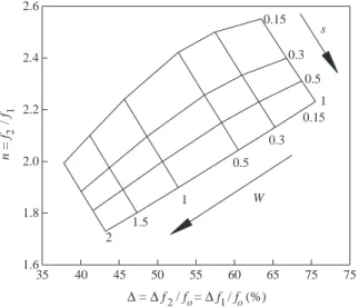
35 1.6 40 45 50 55 60 65 75 75 1.8 2.0 2.2 2.4 2.6 W 2 1.5 1 0.5 0.3 s 0.15 0.3 1 0.5 0.15 n = f / f 2 1 2 o 1 o ∆ = ∆ f / f = ∆ f / f (%)
Figure 5. Frequency ratio and bandwidth design graph for coupled three-line resonators. Substrate: εr = 10.2, thickness = 1.27 mm. W
Figure 5 draws the frequency ratio and bandwidth design graph for of the dual-band bandpass filter with coupled three-line resonators. Table 1 compares the realizable frequency ratio n and bandwidths ∆ by the three configurations.
4. CROSS-SHAPED ADMITTANCE INVERTER
All the stubs, coupled-line, and coupled three-line in Figures 1, 3 and 4 are quarter-wavelength long at fo. Thus, a periodic bandpass response
in the frequency axis can be expected, and the dual-wideband response will repeat itself at 3fo, 5fo, . . ., etc. Figure 6 shows a typical frequency
Table 1. Realizable frequency ratio n = f2/f1 and fractional
bandwidth ∆. Microstrip circuit substrate: εr = 10.2, thickness
= 1.27 mm.
Structure\Parameters nmin nmax ∆min (%) ∆max (%)
Shunt Open and
Shorted Stubs (Figure 1) 2.14 3.54 31.9 57.3 Coupled-Line Resonator (Figure 3) 1.55 2.26 37.7 70.0 Coupled Three-Line Resonator (Figure 4) 1.73 2.55 38.2 75.0 0 -20 -40 -60 |S |, (dB) 11 | | 21 S 1- α 1 1+ α 2 3- α 3 3+ α Normalized Frequency ( f / f )o |S11| |S21|
Figure 6. Typical frequency response of a dual-wideband bandpass filter. Zsc= 25 Ω, Zoc= 100 Ω, Zo = 50 Ω. θ = π/2 at fo.
response of a dual-band bandpass filter. It can be validated that for the structure in Figure 1 the two-port parameters can be calculated by
S11 = (1 + y1 − yeyo e)(1 + yo) (7a) S21 = yo− ye (1 + ye)(1 + yo) (7b) ye = YYin o + j tanθ 2 (7c) yo = Yin Yo − j cotθ 2 (7d)
where Yo= Zo−1 and Yin is given in (1). The center frequencies of the
two passbands can be written as follows:
f1 = (1 − α)fo (8a) f2 = (1 + α)fo (8b) where α = n − 1 n + 1 (8c) n = f2/f1 (8d)
Also, the center frequencies of the spurious passbands around 3fo can
be represented by
f10 = (3 − α)fo (9a)
f20 = (3 + α)fo (9b)
The targets to be suppressed for stopband extension are the spurious bands at f10 and f20.
The main transmission line section between the stubs in Figures 1, 3 and 4 has an electrical length of 90 degrees. It plays as an admittance inverter in filter design. Obviously, when the operation
Z ,90 @ f o
o
o
Port 1 Port 2 Port 1 Port 2
Z , θ @ f 1 1 o
Z , θ @ f 2 2 o
Ζ , θ @ f 1 1 o
Z , θ @ f 2 3 o
(a) (b)
Figure 7. Admittance inverters. (a) Conventional admittance inverter. (b) Proposed cross-shaped admittance inverter.
frequency is increased to three times the center frequency, the electrical length of this section becomes 270◦ or –90◦. It means the inverter
also provides coupling between the two side resonators at 3fo. In this section, a cross-shaped admittance is proposed to substitute this inverter, and to produce two transmission zeros at around 3foto cancel
the spurious passbands.
Figure 7(a) shows the conventional admittance inverter. The two-port Z-parameters of the inverter can be obtained through the even and odd analysis:
Zino = jZo (10a)
Zine = −jZo (10b)
Figure 7(b) shows the proposed cross-shaped inverter, consisting of a 2θ1-section with two open stubs shunt at its center. The main section
has characteristic impedance Z1 and the two open stubs have identical
characteristic impedance Z2 but different electrical lengths θ2 and θ3.
The input impedances of the proposed inverter with even and odd symmetric planes in the middle can be derived as
Zino = jZ1tan θ1 (11a)
Zine = −jZ12ZZ 2− Z1tan θ1(tan θ2+ tan θ3) 1(tan θ2+ tan θ3) + 2Z2tan θ1
(11b) Enforcing (11a) equal to (10a) and (11b) identical to (10b), we obtain
Z1 = Zocot θ1 (12a)
Z2 = Zo
tan θ2+ tan θ3 1 − tan2θ
1 (12b)
These equations indicate that if Z1 and Z2 are calculated based on
given θ1, θ2and θ3, the cross-shaped inverter can be exactly equivalent
to an ideal admittance inverter at the design frequency fo. The values
of θ2 and θ3 are chosen to generate two transmission zeros at f10 and f0
2 in (9) where the electrical lengths θ2 and θ3 are 90 degrees:
θ2 = 90◦/(3 − α) (13a)
θ3 = 90◦/(3 + α) (13b)
5. SIMULATION AND MEASUREMENT
Two experimental dual-wideband filters are fabricated and measured for validations. The circuits are fabricated on a substrate with
εr = 10.2 and thickness h = 1.27 mm. The simulation work is
layout of the first circuit with coupled-line resonators, and Figure 8(b) is the photograph of the measured circuit. It is designed to have
f1 = 900 MHz, f2 = 1575 MHz, and fractional bandwidth ∆ = 39%. The electrical lengths of the two shunt open-stubs of the cross-shaped inverter are θ2 = 32.97◦ and θ3 = 27.52◦ at fo. Given θ1 = 30◦,
s W1 1 Wc2 2 W2 Wc1 3 1 Wc3 |S |, | S | (d B) 11 2 1 |S 11| |S 21| Measurement Simulation 28.9 dB , 3.97 fo -60 -50 -40 -30 -20 -10 0 0 1 2 3 4 5 Frequency (GHz) (b) 4 c 2 3 c (a) (c)
Figure 8. Performance of the dual-wideband bandpass filters with coupled-line resonators. (a) Circuit layout. (b) |S11| and |S21|
responses. (c) Photograph of the experimental circuit. Geometric parameters: `1 = 23.89 mm, `2 = 23.10 mm, `3 = 0.65 mm, `4 =
3.50 mm, W1 = 1.76 mm, W2 = 1.19 mm, s1 = 0.15 mm, `c1 = 8.54 mm, `c2 = 9.32 mm, `c3 = 7.86 mm, Wc1 = 0.54 mm, Wc2 = 0.56 mm, Wc3= 0.56 mm.
s W1 Wc2 2 W2 Wc1 3 1 Wc3 4 |S |, | S (dB) 11 1 -60 -50 -40 -30 -20 -10 0 0 1 2 3 4 5 Frequency (GHz) 2 | (a) (c) Measurement Simulation 28.9 dB 4.03 fo |S |11 |S |21 1 3 2 c c , (b)
Figure 9. Performance of the dual-wideband bandpass filters with coupled three-line resonators. (a) Circuit layout. (b) Simulated and measured |S11| and S21| responses. (c) Photograph of the experimental
circuit. Geometric parameters: `1 = 22.09 mm, `2 = 21.30 mm,
`3 = 0.65 mm, `4 = 3.50 mm, W1 = 1.97 mm, W2 = 1.19 mm, s1 = 0.15 mm, `c1 = 7.89 mm, `c2 = 8.73 mm, `c3 = 7.09 mm, Wc1 = 0.52 mm, Wc2 = 0.56 mm, Wc3 = 0.56 mm.
Z1 = 86.60 Ω and Z2 = 87.72 Ω are calculated by (12). Figure 8(c)
compares the measured with the simulated responses. They show good agreement. The insertion losses at f1 and f2 are −0.987 dB and
−1.318 dB, respectively. The measured bandwidths are ∆1 = 37.98% and ∆2 = 36.94%, showing small deviations from the design. The two transmission zeros created by the cross-shaped inverter are at 3.14 and 4.21 GHz As shown in Figure 8(c), the spurious passbands near 3fo
are successfully suppressed. The upper stopband is extended up to 4.91 GHz (3.97fo) for a reference insertion loss level of 28.9 dB.
Figure 9(a) shows the layout of the second experimental dual-wideband filter with the coupled three-line resonators, and Figure 9(b) depicts the photograph of the measured circuit. It is designed to have f1 = 900 MHz, f2 = 1800 MHz, and bandwidth ∆ = 38%.
The electrical lengths θ2 = 33.71◦ and θ3 = 27.03◦ are chosen.
Let θ1 = 30◦, and Z1 = 86.60 Ω and Z2 = 88.29 Ω can be known
from (12). Figure 9(c) draws the simulated and measured responses. The measured insertion losses at 900 and 1800 MHz are −1.38 dB and
−1.49 dB, respectively. The two measured bandwidths are ∆1 =
38.52% and ∆2 = 37.04%, showing negligible deviations from the design. The upper stopband is extended to 5.44 GHz (4.03fo) for a reference insertion loss level of 25 dB, achieved by the transmission zeros generated by the cross-shaped inverter. The measured results match with the simulated responses quite well.
The circuit layout is developed based on the design graph in Figure 5, where effect of the cross-shaped admittance inverter on the coupling between the coupled three-line resonators is excluded. The differences between the designed and measured ∆1and ∆2are less than
0.5% and 1%, respectively. These are negligible deviations as compared with the designed 38%. This reflects the fact that the insertion of the cross-shaped admittance inverter has little influence on the design graphs in Figures 3 and 5.
6. CONCLUSION
Coupled-line and coupled three-line resonators are proposed and validated as good candidates for design of dual-wideband bandpass filters. These two resonators are used to play the role of an open stub and shorted stub shunt at the main transmission line. The fractional bandwidths and ratios of the two center frequencies realizable by these two types of resonator are compared with those of the design with shunt stubs. One of the advantages of the two proposed structures is that half of the area can be saved. A cross-shaped admittance inverters are proposed to create transmission zeros for upper stopband extension. The measured results not only confirm the analysis but also show good agreement with the simulation results obtained by commercial software package.
ACKNOWLEDGMENT
This work was supported in part by the National Science Council, Taiwan, under Grant NSC 98-2211-E-009-032-MY2 and Grant NSC 100-2221-E-182-059-MY2, and in part by the Chang Gung University, Taiwan, under Grant UERPD2A0021.
REFERENCES
1. Pozar, D. M., Microwave Engineering, 3rd Edition, Wiley, New York, 2005.
2. Kuo, J.-T. and H.-S. Cheng, “Design of quasi-elliptic function filters with a dual-passband response,” IEEE Microw. Wireless
Compon. Lett., Vol. 14, No. 10, 472–474, Oct. 2004.
3. Chiou, Y.-C. and J.-T. Kuo, “Planar multiband bandpass filter with multimode stepped-impedance resonators,” Progress In
Electromagnetics Research, Vol. 114, 129–144, 2011.
4. Kuo, J.-T., T.-H. Yeh, and C.-C. Yeh, “Design of microstrip bandpass filters with a dual-passband response,” IEEE Trans.
Microw. Theory Tech., Vol. 53, No. 4, 1331–1336, Apr. 2005.
5. Ma, D., Z.-Y. Xiao, L. Xiang, X. Wu, C. Huang, and X. Kou, “Compact dual-band bandpass filter using folded SIR with two stubs for WLAN,” Progress In Electromagnetics Research, Vol. 117, 357–364, 2011.
6. Chen, C.-Y. and C.-Y. Hsu, “A simple and effective method for microstrip dual-band filters design,” IEEE Microw. Wireless
Compon. Lett., Vol. 16, No. 5, 246–248, May 2006.
7. Yang, R.-Y., K. Hon, C.-Y. Hung, and C.-S. Ye, “Design of dual-band dual-bandpass filters using a dual feeding structure and embedded uniform impedance resonators,” Progress In Electromagnetics
Research, Vol. 105, 93–102, 2010.
8. Zhang, X. Y., J.-X. Chen, Q. Xue, and S.-M. Li, “Dual-band bandpass filters using stub-loaded resonators,” IEEE Microw.
Wireless Compon. Lett., Vol. 17, No. 8, 583–585, Aug. 2007.
9. Mondal, P. and M. K. Mandal, “Design of dual-band bandpass filters using stub-loaded open-loop resonators,” IEEE Trans.
Microw. Theory Tech., Vol. 56, No. 1, 150–155, Jan. 2008.
10. Chen, C.-H., C.-S. Shih, T.-S. Horng, and S.-M. Wu, “Very miniature dual-band and dual-mode bandpass filter designs on an integrated passive device chip,” Progress In Electromagnetics
11. Chen, C.-Y. and C.-C. Lin, “The design and fabrication of a highly compact microstrip dual-band bandpass filter,” Progress
In Electromagnetics Research, Vol. 112, 299–307, 2011.
12. Yim, H.-Y. A. and K.-K. M. Cheng, “Novel dual-band planar resonator and admittance inverter for filter design and applications,” IEEE MTT-S Int. Microwave Symp. Dig., 2187– 2190, Jun. 2005
13. Liu, A.-S., T.-Y. Huang, and R.-B. Wu, “A dual wideband filter design using frequency mapping and stepped-impedance resonators,” IEEE Trans. Microw. Theory Tech., Vol. 56, No. 12, 2921–2929, Dec. 2008.
14. Kuo, J.-T., M. Jiang, and H.-J. Chang, “Design of parallel-coupled microstrip filters with suppression of spurious resonances using substrate suspension,” IEEE Trans. Microwave Theory Tech., Vol. 52, No. 1, 83–89, Jan. 2004.
15. Kuo, J.-T., W.-H. Hsu, and W.-T. Huang, “Parallel-coupled microstrip filters with suppression of harmonic response,” IEEE
Microw. Wireless Compon. Lett., Vol. 12, No. 10, 383–385,
Oct. 2002.
16. Jiang, M., M.-H. Wu, and J.-T. Kuo, “Parallel-coupled microstrip filters with over-coupled stages for multispurious suppression,”
IEEE MTT-S Int. Microwave Symp. Dig., 687–690, Jun. 2005.
17. Kuo, J.-T. and E. Shih, “Microstrip stepped-impedance resonator bandpass filter with an extended optimal rejection bandwidth,”
IEEE Trans. Microw. Theory Tech., Vol. 51, No. 5, 1554–1559,
May 2003.
18. Kuo, J.-T. and H.-P. Lin, “Dual-band bandpass filter with improved performance in extended upper rejection band,” IEEE
Trans. Microw. Theory Tech., Vol. 57, No. 4, 824–829, Apr. 2009.
19. Mokhtaari, M., K. Rambabu, J. Bornemann, and S. Amari, “Advanced stepped-impedance dual-band filters with wide second stopbands,” Proc. Asia-Pacific Microw. Conf., 2285–2288, 2007. 20. Kuo, J.-T., “Accurate quasi-TEM spectral domain analysis
of single and multiple coupled microstrip lines of arbitrary metallization thickness,” IEEE Trans. Microw. Theory Tech., Vol. 43, No. 8, 1881–1888, Aug. 1995.
21. Fan, C.-Y., “Dual-wideband bandpass filters with stopband extension,” M.S. thesis, National Chiao Tung University, Hsinchu, Taiwan, Jun. 2010.
![Figure 1 depicts a second-order dual-band bandpass filter with parallel open-circuit and shorted stubs [12, 13]](https://thumb-ap.123doks.com/thumbv2/9libinfo/7589108.127186/4.681.185.510.543.814/figure-depicts-second-bandpass-filter-parallel-circuit-shorted.webp)