In Situ Doped Source/Drain for Performance
Enhancement of Double-Gated Poly-Si
Nanowire Transistors
Wei-Chen Chen, Horng-Chih Lin, Senior Member, IEEE, Yu-Chia Chang,
Chuan-Ding Lin, and Tiao-Yuan Huang, Fellow, IEEE
Abstract—A poly-Si nanowire (NW) thin-film transistor
config-ured with the double-gated scheme was fabricated and character-ized. The fabrication process features the clever use of selective plasma etching to form a rectangular NW underneath a hard mask. In this paper, we show that replacing the original ion-implanted poly-Si with in situ doped poly-Si for the source/drain significantly enhances the device performance, including steeper subthreshold swing (SS), larger on/off current ratio, and re-duced series resistance. In particular, the SS is improved to a record-breaking low value of 73 mV/dec, which, to the best of our knowledge, is the most ideal ever reported for a poly-Si based device. The new NW transistors with such excellent switching properties are highly promising for reducing power consumption and operational voltage in practical circuit applications.
Index Terms—Field-effect transistor, in situ doping, leakage,
multiple gate, nanowire (NW), polycrystalline-Si (poly-Si). I. INTRODUCTION
P
OLYCRYSTALLINE-Si (poly-Si) thin-film transistors (TFTs), which act as an important building block in drivers of liquid crystal display (LCD), have become very attractive for future 3-D electronics integration [1]. Compared with single-crystalline Si-based microelectronics, where expensive sub-strates are inevitable, high- performance TFTs have emerged as a promising alternative for microelectronics employing glass and plastic substrates, where flexibility and light weight are primarily preferred [2]. It would be quite a breakthrough if poly-Si TFTs could display comparable performance to single-crystalline Si-based devices on account of its low fabrica-tion cost. However, the fine-grained structure that is inherent in poly-Si significantly degrades the carrier mobility [3] and limits its adoption and proliferation in advanced ultra large-scale integration (ULSI) technologies. To address this intrinsic material issue, a plethora of recrystallization methods for grain enlargement have been proposed, with solid-phasecrystalliza-Manuscript received November 5, 2009; revised March 18, 2010; accepted March 19, 2010. Date of publication May 24, 2010; date of current version June 23, 2010. This work was supported in part by the National Science Council under Contract NSC 96-2221-E-009-212-MY3. The review of this paper was arranged by Editor M. Reed.
W.-C. Chen, H.-C. Lin, Y.-C. Chang, and T.-Y. Huang are with the Depart-ment of Electronics Engineering and Institute of Electronics, National Chiao Tung University, Hsinchu 300, Taiwan (e-mail: [email protected]).
C.-D. Lin is with the National Nano Device Laboratories, Hsinchu 300, Taiwan.
Color versions of one or more of the figures in this paper are available online at http://ieeexplore.ieee.org.
Digital Object Identifier 10.1109/TED.2010.2049227
tion (SPC) [4], metal-induced lateral crystallization (MILC) [5], and excimer laser annealing (ELA) [6] being the most commonly used. To continue the scaling trend while simultane-ously improving poly-Si device characteristics, extrinsic mod-ification, e.g., ultrathin body structures, provides an effective solution for the aforementioned problem. From a microscopic perspective, 1-D nanowire (NW) structure also offers a unique platform for physical properties not easily observed in conven-tional devices. The unique characteristics of large surface-to-volume ratio and high sensitivity to surface conditions have rendered NW a functional device suitable for biosensing [7] and nonvolatile memory [8] applications. Among the various methods for NW fabrication, top–down approaches avoid the misalignment and hard-to-manipulate issues that are frequently encountered in bottom–up processes and, meanwhile, are more compatible with modern CMOS process flows. Moreover, when combined with multiple-gated scheme, the fabricated device exhibits enhanced drive current and steeper subthreshold swing (SS) due to improved control of electrostatic potential in the channel, as demonstrated in various works, including FinFET [9], omega gate [10], trigate [11], and gate all around [12]. Meanwhile, CMOS-compatible performance has also been achieved using poly-Si NW devices [13], [14]. To this end, we had presented several innovative top–down approaches for forming poly-Si NWs using conventional I-line-based litho-graphy [15]–[17]. Most recently, a selective plasma-etching technique was adopted to fabricate devices with rectangular NW channels, thus alleviating the sharp corners in previous triangular-shaped NW devices [18]. In the original fabrication process, source/drain (S/D) regions were formed by a low-energy ion implantation so that dopants were situated near the top surface to avoid compromising the gate controllabil-ity caused by inadvertent channel doping [15]. Although this method attains good gate control over NW channels, it still unavoidably leads to slight channel doping by the tail part of dopant distribution and is achieved at the expense of S/D resistance, because only a small portion of S/D is heavily doped. In addition, as reported in one of our previous studies [19], the major leakage current is identified to be the gate-induced leakage current (GIDL) that originated in the gate/drain overlap area in the structure. Because the portion of drain that is closest to the gate is only moderately doped, this approach makes band-to-band tunneling (BTBT) much easier to occur and results in severe leakage current. To alleviate this problem,
here, we propose a modified method for fabricating devices with identical structure, except that the S/D regions are more uniformly and heavily doped by employing an in situ doping approach. This way, the S/D resistance and gate controllability are no longer compromised, leading to a win–win situation.
The content of this paper is arranged as follows. In Section II, the condition and results of selective plasma etching are discussed. Section III then describes process flows for devices with implanted and in situ doped S/D, respectively, followed by electrical characterization in Section IV. Finally, a brief conclusion is given in Section V.
II. INVESTIGATION OFSELECTIVE
PLASMA-ETCHINGCONDITIONS
The main feature in this structure lies in the fact that a sub-100-nm cavity could be formed by isotropic plasma etching using a high-density plasma (HDP) etching apparatus. In this paper, a transformer-coupled plasma (TCP) reactor manufac-tured by Lam Research was used, which operates by inductively coupling RF power to plasma. This tool is equipped with two RF power generators. The top source RF power generates plasma and determines ion density, whereas the bottom bias RF power is responsible for controlling the ion bombardment energy. In other words, ion density and energy are indepen-dently controlled in this reactor, thus solving the inflexibility and poor efficiency of conventional capacitively coupled reac-tors. In contrast to the typical anisotropic RIE process in an HDP etching tool, the sub-100-nm cavity-forming technique is accomplished by turning off the bottom bias. This way, the bombarding energy of ions would be reduced to achieve high etching selectivity between poly-Si and the other layers.
The process flow of the proposed two-step n+poly-Si etch-ing scheme is depicted in Fig. 1(a). A stack of layers that comprise thermal oxide/nitride/n+poly-Si/nitride was sequen-tially deposited on a 6-in Si wafer. Next, the top nitride and n+ poly-Si stack were patterned by anisotropic etching in a TCP reactor. Fig. 1(b) displays a scanning electron microscope (SEM) picture taken after this step. It is observed that the final etching profile is anisotropic. This result is because chlorine etching mainly proceeds in an ion-induced manner; therefore, the etched profile is essentially anisotropic. Following photore-sist stripping, the wafer was loaded into the same reactor for selective and isotropic n+poly-Si plasma etching. In this step, fluorine-containing gas SF6 is added, along with chlorine, to increase the isotropic etching component, with the result shown in Fig. 1(c). It has been well known that poly-Si can be etched by fluorine-based etchants because of the high volatility of SiF4[20]. Meanwhile, F radicals are usually produced in large quantities in plasma, along with little polymer formation; there-fore, the final profile will be relatively isotropic. This image indicates that fluorine addition greatly enhances the isotropic profile and demonstrates high selectivity with respect to nitride layer. This approach is quite reasonable, because in addition to rendering the motion of bombarding ions a random manner, setting the bias power to zero improves the etching selectivity of poly-Si against other materials. It is noted that this isotropic etching is performed in the same reactor as that of anisotropic
Fig. 1. (a) Test structure used for investigating selective plasma-etching conditions. Cross-sectional SEM image after plasma etching using (b) chlorine and (c) chlorine and sulfur hexafluoride gases.
etching, suggesting the compatibility and convenience of this novel procedure. To demonstrate the merit of this approach in fabricating decananometer NWs, Fig. 2 displays the lateral encroaching depth as a function of etching time as characterized by SEM, indicating that the NW dimension could flexibly be controlled. In fact, it is very hard to produce the same result
Fig. 2. Measured lateral etching depth as a function of etching time. The inset gives the definition of lateral etching depth.
Fig. 3. Schematic process flow for the double-gated NWTFT with implanted S/D. (a) Sequential deposition of 200-nm thermal oxide, 50-nm nitride, 100-nm N+poly-Si, and 50-nm nitride on a 6-in Si wafer. First gate stack patterning
was then performed. (b) Selective plasma etching of the first gate. (c) First gate dielectric (20-nm LPCVD TEOS oxide) and 100-nm amorphous Si-layer deposition followed by 600◦C annealing at N2ambient for 24 h (SPC). (d) S/D
implantation with energy 15 keV and dosage 5× 1015cm−2. (e) Simultaneous
definition of NW channels and S/D regions using dry etching. (f) Second gate stack (20-nm LPCVD TEOS oxide and 100-nm N+poly-Si) deposition and
definition.
each time for etching with duration of less than 10 s, because the condition of glow discharge is not yet stable in such a short period. However, it is believed that the proposed method will have more reproducible results, provided that the etching condition is optimized. In other words, by carefully adjusting the flow rate of source gas, RF power, and etching time, the structural parameter can be easily and reliably shrunk into the decananometer regime.
III. DEVICESTRUCTURES ANDFABRICATION
The devices characterized in this paper employ a double-gated configuration, where NW channels are formed under-neath a nitride hard mask. In this paper, two types of devices with different S/D formation techniques are compared. For the implanted S/D type, a detailed device fabrication process was elaborated in [18] and is briefly illustrated in Fig. 3. The gradual variation of colors in the S/D regions in Fig. 3(e) highlights that the doping concentration is not uniform and decreases
from the topmost surface toward the channel regions. Fig. 4 schematically illustrates the modified process for which S/D is formed by using in situ doping technique. The process flow is identical to that shown in Fig. 3 down to the SPC step. Then, without any photolithographic process, a spacer-like portion of poly-Si along the sidewall of the first gate, whose purpose will later be discussed, was created by carrying out a dry etching step with endpoint detection. Subsequently, in situ phosphorus doped poly-Si was deposited by low-pressure chemical vapor deposition (LPCVD) at 550◦C and 600 mtorr using 200 sccm PH3 and 1 slm SiH4, followed by S/D region patterning. This way, because there was no implantation involved and NW channels underneath the hardmask were protected by the spacer-shaped poly-Si from being exposed to PH3 in the
in situ doped poly-Si deposition step, the entire S/D regions
were heavily doped, whereas the NWs remained unscathed (i.e., undoped). The second gate stack was then deposited and patterned to complete the device. Dopant activation was fulfilled using the thermal budget of processing steps after implantation, including the deposition of the second gate stack [20-nm LPCVD tetraethoxysilane (TEOS) oxide and 100-nm N+ poly-Si] and 350-nm passivation LPCVD TEOS oxide, approximately amounting to 700◦C annealing for 8 h. To avoid possible dopant diffusion into NWs, we intentionally left a spacer-like poly-Si instead of directly forming rectangular NWs as shown in Fig. 3(e) so that, even if diffusion occurs, this spacer-like portion, which is part of S/D, is doped first before channel doping happens. In addition, channel doping should not be of significance, because the highest temperature of the subsequent thermal budget is merely 700 ◦C in TEOS oxide deposition step.
IV. ELECTRICALCHARACTERISTICS
Fig. 5 depicts a transmission electron microscope (TEM) picture of the proposed device, from which the thickness of NW (or the width of NW between the two gate dielectrics) is observed to be 22 nm. Transfer characteristics for the control device with implanted S/D are shown in Fig. 6. Channel length and gate oxide thickness are 1 μm and 20 nm, respectively. Due to the unique feature associated with two independent gates in the proposed structure, device operation can be categorized into SG-1, SG-2, and DG modes. In particular, the SG-1 and SG-2 modes refer to the scheme with the first or second gate acting as the sweeping gate, respectively, whereas the other one is grounded. Under the DG mode, two gates are connected together and serve as a single sweeping gate. It can be observed that DG operation demonstrates much enhanced performance in terms of lower threshold voltage (VTH), higherONcurrent (ION), and steeper SS (i.e., 89 mV/dec) due to its stronger elec-trostatic gate controllability over channels. It has been stated in [18] that additional nongated routes would have significantly increased the series resistance of the SG-1 mode. However, the nearly symmetric transfer curves between the SG-1 and SG-2 modes indicate that this detrimental effect related to the NW thickness is dramatically reduced. Impacts of NW thickness on device performance are exhibited in Fig. 7, where devices with three different NW dimensions are compared. The size
Fig. 4. Schematic process flow for the double-gated NWTFT with in situ doped S/D. (a) Sequential deposition of 200-nm thermal oxide, 50-nm nitride, 100-nm N+poly-Si, and 50-nm nitride on a 6-in Si wafer. First gate stack patterning was then performed. (b) Selective plasma etching of the first gate. (c) First gate
dielectric (20-nm LPCVD TEOS oxide) and 100-nm amorphous Si-layer deposition followed by 600◦C annealing at N2ambient for 24 h (SPC). (d) Dry etching
to form NWs underneath the hard mask and a spacer-like portion of poly-Si along the sidewall of the first gate. (e) Deposition of 100-nm in situ phosphorus doped poly-Si. (f) Simultaneous definition of NW channels and S/D regions using dry etching. (g) Second gate stack (20-nm LPCVD TEOS oxide and 100-nm N+poly-Si) deposition and definition.
Fig. 5. TEM image of an independent double-gated transistor that shows 22-nm NW thickness.
Fig. 6. Transfer characteristics of a fabricated device with implanted S/D.
dependency has been briefly discussed in [18], in which it was found that smaller NW thickness led to more improvement in DG operation. According to our recent calculation results [21], the major cause of enhanced DG performance over SG modes is its stronger grain boundary barrier modulation ability. Because reduced NW thickness enables gate coupling to a larger extent,
Fig. 7. Size dependency of transfer characteristics for devices with NW thickness of 53, 42, and 22 nm.
Fig. 8. Transfer characteristics of a fabricated device with in situ doped S/D.
this phenomenon manifests itself in steeper SS of DG operation, as evidenced in Fig. 7.
Fig. 8 shows the transfer characteristics of the device with
in situ doped S/D with structural parameters nominally identical
to the device characterized in Fig. 6. TheON/OFFcurrent ratio
Fig. 9. Fluctuation analysis of devices with (a) in situ doped S/D and (b) implanted S/D.
magnitude higher than that for the device with implanted S/D in Fig. 6. Furthermore, SS is enhanced from 89 mV/dec to 73 mV/dec under the DG mode when in situ doping technique is adopted. Note that, to the best of our knowledge, this result is the best value ever reported for a poly-Si based device. To prove that the aforementioned characteristics are representative of the whole picture, we have conducted fluctuation analysis in Fig. 9 by showing transfer curves of 20 devices with similar characteristics collected from a total of 29 and 26 devices for implanted and in situ doped types, respectively, amounting to 69% and 77% chip yield. Those not shown have either larger than 100-mV/dec SS or are simply not functional. As shown in the figure, the variation is not severe, and this result suggests the good uniformity offered by the selective plasma-etching technique. The mean value and standard deviation of VTH at
VD= 0.5 V for in situ doped and implanted devices are 0.33 V,
35 mV and 0.31 V, 46 mV, respectively. SS distribution with respect to channel length is shown in Fig. 10 for in situ doped devices. Under DG operation, excellent immunity to the short-channel effect is observed, and the characterized devices demonstrate tight distribution.
Major device characteristics of both types of devices shown in Figs. 6 and 8 are summarized in Table I. The difference in
VTH between the two devices is small and within the mea-sured fluctuation value. Aside from this, all the other device characteristics of the in situ doped type are superior to the implanted type. For the SS improvement, in situ doping avoids unintentional channel doping by ion implantation. Meanwhile,
Fig. 10. SS as a function of channel length for the in situ doped device. TABLE I
SUMMARY OF THEMAJORCHARACTERISTICS OFDEVICESWITH
IMPLANTED(FIG. 6)ANDIn Situ DOPEDS/D (FIG. 8)
Fig. 11. Output characteristics comparison under the DG mode for devices with implanted and in situ doped S/D.
more uniform and highly activated doping concentration gives rise to largerON/OFFcurrent ratio due to smaller series resis-tance and reduced BTBT probability. This statement is further evidenced in the output characteristics shown in Fig. 11, where only those under the DG mode are displayed for clarity. At
VG− VTH= VD= 5 V, the saturation current improvement
over the implanted control device is 48%. For the SG-1 and SG-2 modes, under the same bias condition, the improvement is 107% and 5.4%, respectively (data not shown). The large
Fig. 12. Extraction of S/D series resistance showing five times reduction with the adoption of in situ doped S/D.
Fig. 13. ION–IOFF statistical analysis comparison between devices with
implanted and in situ doped S/D.
disparity between the extent of improvement for the two SG modes is related to their different current paths from the source to the drain. If S/D is formed by ion implantation, carriers under the SG-1 mode must transport across a long distance of only moderately doped S/D before reaching the topmost portion of S/D where the resistivity is the smallest. Under the SG-2 mode, because the outer channel surface controlled by the second gate is closer to the most heavily doped S/D regions than the first gate, it is easier for carriers to reach the topmost S/D without experiencing significant series resistance. This condition explains why output current is dramatically improved for the SG-1 mode, whereas it is only slightly increased for the SG-2 mode when in situ doping results in S/D with lower series resistance. By using the measured output curve data, the total resistance can be plotted against channel length [22], as shown in Fig. 12. It is shown that there is approximately five times reduction in series resistance from 45 KΩ to 8.1 KΩ when S/D is formed by in situ doping.
For statistical analysis, the ION–IOFF plot is shown in Fig. 13. At a fixed IOFFequal to 3 pA, the in situ doping method results in 252% ION improvement by increasing ION from 1.46 μA to 5.14 μA, suggesting the significance of S/D engi-neering for performance enhancement.
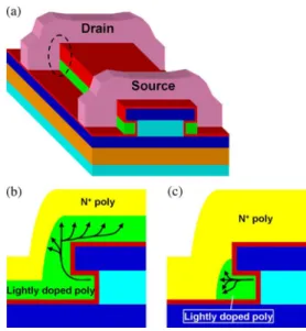
Fig. 14. (a) Schematic of the device structure before the second gate stack deposition. GIDL current conduction paths in the circled areas of (a) are depicted for (b) implanted S/D and (c) in situ doped S/D type devices.
The reason for the drastic GIDL current reduction with the adoption of in situ doped S/D is now discussed. There does not exist an absolute relationship between the GIDL current and S/D doping concentration [23]. At a given gate and drain bias, very low S/D doping concentration would lead to severe band bending at the drain/oxide interface. However, the depletion width is also large because of the low doping concentration. This condition increases the tunneling width; therefore, the BTBT probability is diminished. On the other hand, for the highly doped case, although the depletion width is extremely small, the band bending is also curbed, which corresponds to the in situ doped S/D scenario in this paper. Taking these factors into account, it is straightforward to understand that moderate S/D doping concentration is the most susceptible to GIDL, and this approach fits the implanted S/D type device. The GIDL current difference can be explained from another perspective in terms of the effective conduction area of leakage current in Fig. 14. To make it more lucid, Fig. 14(a) is the schematic structure before the second gate stack deposition. Fig. 14(b) and (c) shows, respectively, the major leakage current conduc-tion paths in the gate/drain overlap regions that correspond to the circled areas in Fig. 14(a) for the implanted and in situ doped S/D type devices. Due to the dissimilar doping profiles, the lightly doped region, where GIDL easily occurs, is much more widespread in Fig. 14(b) than in Fig. 14(c), posing as another factor that accounts for the leakage current difference. In addition, the lightly doped areas are essentially nongated and behave as additional transport barriers, which can also explain the improvement of SS by the in situ doping technique.
V. CONCLUSION
In this paper, we have investigated the performance enhance-ment of a double-gated poly-Si NW transistor with in situ doped S/D, which can be fabricated by a simple selective plasma-etching process without resorting to sophisticated lithographic tools. Because of the elimination of ion implantation that is
likely to cause excessive dopant incorporation into the channel, the in situ doping technique has been shown to improve the SS down to 73mV/dec. We believe that this result is the best SS ever reported for any poly-Si channel based device. Due to the higher dopant concentration offered by the proposed method, five times reduction in series resistance is achieved compared with the control device, and leakage current that results from GIDL is substantially suppressed. The proposed NW device with excellent switching properties appears to be very promising for reducing the operational voltage and power consumption in future circuit applications.
ACKNOWLEDGMENT
The authors would like to thank the National Nano Device Laboratories (NDL) and the Nano Facility Center (NFC) of the NCTU for assistance in device fabrication.
REFERENCES
[1] E. K. Lai, H. T. Lue, Y. H. Hsiao, J. Y. Hsieh, C. P. Lu, S. Y. Wang, L. W. Yang, T. Yang, K. C. Chen, J. Gong, K. Y. Hsieh, R. Liu, and C. Y. Lu, “A multilayer stackable thin-film transistor (TFT)NAND-type flash memory,” in IEDM Tech. Dig., Dec. 2006, pp. 41–44.
[2] B. Crone, A. Dodabalapur, Y.-Y. Lin, R. W. Filas, Z. Bao, A. LaDuca, R. Sarpeshkar, H. E. Katz, and W. Li, “Large-scale complementary inte-grated circuits based on organic transistors,” Nature, vol. 403, no. 6769, pp. 521–523, Feb. 2000.
[3] J. Y. W. Seto, “The electrical properties of polycrystalline silicon films,”
J. Appl. Phys., vol. 46, no. 12, pp. 5247–5254, Dec. 1975.
[4] R. B. Iverson and R. Reif, “Stochastic model for grain size versus dose in implanted and annealed polycrystalline silicon films on SiO2,” J. Appl. Phys., vol. 57, no. 12, pp. 5169–5175, Jun. 1985.
[5] S. W. Lee, T. H. Ihn, and S. K. Joo, “Fabrication of high-mobility p-channel poly-Si thin-film transistors by self-aligned metal-induced lat-eral crystallization,” IEEE Electron Device Lett., vol. 17, no. 8, pp. 407– 409, Apr. 1996.
[6] J. S. Im and H. J. Kim, “Phase transformation mechanisms involved in excimer laser crystallization of amorphous silicon films,” Appl. Phys.
Lett., vol. 63, no. 14, pp. 1969–1971, Oct. 1993.
[7] Y. Cui, Q. Wei, H. Park, and C. M. Lieber, “Nanowire nanosensors for highly sensitive and selective detection of biological and chemical species,” Science, vol. 293, no. 5533, pp. 1289–1292, Feb. 2001. [8] X. Duan, Y. Huang, and C. M. Lieber, “Nonvolatile memory and
program-mable logic from molecule-gated nanowires,” Nano Lett., vol. 2, no. 5, pp. 487–490, Apr. 2002.
[9] D. Hisamoto, W. C. Lee, J. Kedzierski, H. Takeuchi, K. Asano, C. Kuo, E. Anderson, T. J. King, J. Bokor, and C. Hu, “FinFET—A self-aligned double-gate MOSFET scalable to 20 nm,” IEEE Trans. Electron Devices, vol. 47, no. 12, pp. 2320–2325, Dec. 2000.
[10] F. L. Yang, H. Y. Chen, F. C. Chen, C. C. Huang, C. Y. Chang, H. K. Chiu, C. C. Lee, C. C. Chen, H. T. Huang, C. J. Chen, H. J. Tao, Y. C. Yeo, M. S. Liang, and C. Hu, “25-nm CMOS omega FETs,” in IEDM Tech.
Dig., Dec. 2002, pp. 255–258.
[11] B. Doyle, B. Boyanov, S. Datta, M. Doczy, S. Hareland, B. Jin, J. Kavalieros, T. Linton, R. Rios, and R. Chau, “Trigate fully depleted CMOS transistors: Fabrication, design, and layout,” in VLSI Symp. Tech.
Dig., Jun. 2003, pp. 133–134.
[12] J. Fu, Y. Jiang, N. Singh, C. X. Zhu, G. Q. Lo, and D. L. Kwong, “Polycrystalline Si nanowire SONOS nonvolatile memory cell fabricated on a gate-all-around (GAA) channel architecture,” IEEE Electron Device
Lett., vol. 30, no. 3, pp. 246–249, Mar. 2009.
[13] M. Im, J. W. Han, H. Lee, L. E. Yu, S. Kim, C. H. Kim, S. C. Jeon, K. H. Kim, G. S. Lee, J. S. Oh, Y. C. Park, H. M. Lee, and Y. K. Choi, “Multiple-gate CMOS thin-film transistor with polysilicon nanowire,”
IEEE Electron Device Lett., vol. 29, no. 1, pp. 102–105, Jan. 2008.
[14] S. D. Suk, M. Li, Y. Y. Yeoh, K. H. Yeo, J. K. Ha, H. Lim, H. W. Park, D. W. Kim, T. Y. Chung, K. S. Oh, and W. S. Lee, “Characteristics of sub-5-nm trigate nanowire MOSFETs with single- and poly-Si channels in SOI structure,” in VLSI Symp. Tech. Dig., Jun. 2009, pp. 142–143.
[15] H. C. Lin, M. H. Lee, C. J. Su, T. Y. Huang, C. C. Lee, and Y. S. Yang, “A simple and low-cost method to fabrication TFTs with poly-Si nanowire channel,” IEEE Electron Device Lett., vol. 26, no. 9, pp. 643–645, Sep. 2005.
[16] H. C. Lin, H. H. Hsu, C. J. Su, and T. Y. Huang, “A novel multiple-gate polycrystalline silicon nanowire transistor featuring an inverse-T gate,”
IEEE Electron Device Lett., vol. 29, no. 7, pp. 718–720, Jul. 2008.
[17] H. C. Lin and C. J. Su, “High-performance poly-Si nanowire NMOS transistors,” IEEE Trans. Nanotechnol., vol. 6, no. 2, pp. 206–212, Mar. 2007.
[18] H. C. Lin, W. C. Chen, C. D. Lin, and T. Y. Huang, “Performance enhance-ment in double-gated poly-Si nanowire transistors with reduced nanowire channel thickness,” IEEE Electron Device Lett., vol. 30, no. 6, pp. 644– 646, Jun. 2009.
[19] H. C. Lin, M. H. Lee, C. J. Su, and S. H. Chen, “Fabrication and char-acterization of nanowire transistors with solid-phase crystallized poly-Si channels,” IEEE Trans. Electron Devices, vol. 53, no. 10, pp. 2471–2477, Oct. 2006.
[20] J. D. Plummer, M. D. Deal, and P. B. Griffin, Silicon VLSI Technology:
Fundamentals, Practice, and Modeling. Englewood Cliffs, NJ:
Prentice-Hall, 2000.
[21] H. H. Hsu, H. C. Lin, and T. Y. Huang, “Origins of performance en-hancement in independent double-gated poly-Si nanowire devices,” IEEE
Trans. Electron Devices, vol. 57, no. 4, pp. 905–912, Apr. 2010.
[22] J. G. J. Chern, P. Chang, R. F. Motta, and N. Godinho, “A new method to determine MOSFET channel length,” IEEE Electron Device Lett., vol. EDL-1, no. 9, pp. 170–173, Sep. 1980.
[23] B. Streetman and S. Banerjee, Solid State Electronic Devices, 6th ed. Englewood Cliffs, NJ: Prentice-Hall, 2005.
Wei-Chen Chen was born in Taoyuan, Taiwan, in 1984. He received the B.S. degree in electrophysics in 2006 from the National Chiao Tung University, Hsinchu, Taiwan, where he is currently working toward the Ph.D. degree in the Department of Elec-tronics Engineering and Institute of ElecElec-tronics.
His current research interests include the fabrica-tion and characterizafabrica-tion of nanowire transistors and germanium-based devices.
Horng-Chih Lin (S’91–M’95–SM’01) was born in I-Lan, Taiwan, on August 1, 1967. He received the B.S. degree from the National Central University, Chung-Li, Taiwan, in 1989 and the Ph.D. degree in from the National Chiao Tung University (NCTU), Hsinchu, Taiwan, in 1994.
From 1994 to 2004, he was with the National Nano Device Laboratories (NDL), Hsinchu, Taiwan, where he has been engaged in the research projects of nanoscale device technology development. In 2004, he joined the faculty of NCTU, where he is currently a Professor with the Department of Electronics Engineering and Institute of Electronics. He is the author or a coauthor of more than 200 technical papers in international journals and conference proceedings. His research interests include thin-film transistor (TFT) fabrication and characterization, reliability of CMOS devices, and nanowire device technology.
Dr. Lin served on the Program Committee of the International Reliability Physics Symposium (IRPS) in 2001 and 2002 and the International Conference on Solid State Devices and Materials (SSDM) from 2005 to 2008.
Yu-Chia Chang received the B.S. degree in mate-rials science and engineering in 2007 and the M.S. degree in Department of Electronics Engineering and Institute of Electronics from the National Chiao Tung University, Hsinchu, Taiwan, in 2009.
She is currently with the General-Purpose Device Department, Taiwan Semiconductor Manufacturing Company (TSMC), as an R&D Engineer.
Chuan-Ding Lin was born in Hsinchu, Taiwan, in 1970. He received the B.S. degree from Ming-Hsin Institute of Technology, Hsinchu, Taiwan, in 1992.
He is currently with the National Nano Device Laboratory (NDL), Hsinchu, Taiwan, where he is currently an Engineer who is responsible for process integration and development. He is a coauthor of several technical papers in international conference proceedings. His research interests include dry etch-ing processetch-ing and novel nanodevice fabrication development.
Tiao-Yuan Huang (S’78–M’78–SM’88–F’95) re-ceived the B.S.E.E. and M.S.E.E. degrees from the National Cheng Kung University, Tainan, Taiwan, in 1971 and 1973, respectively. He received the Ph.D. degree from the University of New Mexico, Albuquerque, in 1981.
After serving for two years in the Taiwanese Navy as fulfillment of his conscription duty, he left for the U.S. in 1977. He has worked in the U.S. semicon-ductor industry for 14 years prior to his return to his native country, Taiwan. Since 1995, he has been a professor with the Department of Electronics Engineering and Institute of Electronics, National Chiao Tung University, Hsinchu, Taiwan.
Prof. Huang was the recipient of the Semiconductor International Tech-nology Achievement Award for his invention and demonstration of the fully overlapped lightly doped drain MOS transistors.