國 立 交 通 大 學
材料科學與工程學研究所
博士論文
錫銀銅無鉛銲錫電遷移之研究
Study of Electromigration in Lead-Free
SnAg
3.8
Cu
0.7
Solder
指導教授:陳智 博士
研究生:許穎超
錫銀銅無遷銲錫之電遷移研究
研究生: 許穎超 指導教授: 陳智
國立交通大學材料科學與工程研究所
摘要
在積體電路的銅或鋁導線中所施加的電流密度若高於 10
6A/cm
2,
此電流密度在元件操作溫度約攝氏 100 度的環境下將在陰極造成孔
洞與陽極產生凸起。此種電遷移所造成的破壞將對積體電路可靠度造
成嚴重的影響。在現今的積體電路設計中每一個覆晶封裝的微接點將
承載 0.2 安培的電流,而在未來電流值將會以倍數成長,而覆晶微接
點的尺寸將由 100μm 減小至 50μm,屆時電流密度將到達 10
6A/cm
2此電流密度下將對覆晶微接點造成電遷移破壞。此外,在無鉛話的趨
勢下傳統錫鉛覆晶微接點將被無鉛覆晶微接點所取代。
本研究主要利用覆晶微接點結構試片與 Blech structure 來研究
無鉛錫銀銅銲錫之電遷移行為。在錫銀銅覆晶微接點研究方面,我們
發現破壞發生在陰極的晶片端且造成接點破壞之主要原因為電流擁
擠效應所造成,且在較低之電流密度下破壞發生於介金屬與銲錫之界
於界面中。
在 Blech structure 研究中我們成功的找出錫銀銅銲錫之門檻電
流密度,其值分別為在 80 °C 下為 4.3 × 10
4A/cm
2, 100 °C 下為
3.2
× 10
4A/cm
2,120 °C 下 1.4 × 10
4A/cm
2,這些數值代表錫銀銅銲
錫在該溫度下不會造成電遷移破壞之最高電流密度。錫銀銅銲錫之電
遷移活化能在 80 °C 到 120 °C 區間為 0.45eV。 而其有效電荷系數
Z*在 80℃,100℃,120℃ 分別為-27 , -33,-23。 此外試片經過
退火後發現晶格擴散與晶界擴散具明顯溫度界限。其門檻電流密度值
分別為在 80
°C 下為 4.6 × 10
4A/cm
2, 100
°C 下為 3.9 × 10
4A/cm
2,
120 °C 下 2.2 × 10
4A/cm
2。電遷移活化能在 100 °C 到 140 °C 區間
為 0.8eV。
Abstract of the Dissertation
S
tudy of Electromigration in Lead-Free
SnAg
3.8
Cu
0.7
Solder
Student: Ying-Chao Hsu Advisor: Chih Chen
Department of Materials Science and Engineering
National Chiao Tung University
Electromigration-induced failure of SnAg3.8Cu0.7 flip-chip solder joints was
investyigated with Ti/Cr-Cu/Cu under-bump metallization (UBM) on the chip side and Cu/Ni(P)/Au pad on the BT board side. Electromigration damage was examined under the current density of 2 × 10⁴
A/cm2 at 100 ℃ and 150℃. The failure was found to be at the cathode/chip side and voids were observed at intermetallic compound/solder interface at the cathode chip side. Copper atoms were found to move in the direction of electron flow to form intermetallic compounds at the interface of the solder and the pad metallization on the substrate side due to current stressing.
In addition, eutectic SnAg3.8Cu0.7 solder stripes was investigated in the vicinity
of the device operation temperature of 100 °C by using the edge displacement technique. Measurements were made for relevant parameters for electromigration of the solder, such as drift velocity, threshold current density, activation energy, as well as the product of diffusivity and effective charge number (DZ*). The threshold current densities were estimated to be 4.3 × 10⁴
A/cm2 at 80 °C, 3.2 × 10⁴ A/cm2 at 100 °C, and 1.4 × 10⁴
A/cm2 at 120 °C. These values represent the maximum current densities that the SnAg3.8Cu0.7 solder can carry without electromigration damage at the three
0.45eV in the temperature range of 80℃ to 120℃. The measured products of diffusivity and the effective charge number, DZ*, were -1.8×10⁻¹⁰
cm2/sec at 80℃, -5.0×10⁻¹⁰
cm2/sec at 100℃, and -7.2×10⁻¹⁰ cm2/sec at 120℃. In the pre-annealing specimens, grain boundary and lattice diffusion have a different temperature dependence range from 80 ℃ to 140 ℃ . The threshold current densities were measured to be 4.6 × 10⁴
A/cm2 at 80 °C, 3.9 × 10⁴ A/cm2 at 100 °C, and 2.2 × 10⁴ A/cm2 at 120 °C. The measured activation energy was 0.8eV for the temperature ranges from 100 to 140℃.
誌謝
首先我要感謝我的指導教授陳智老師這四年來不厭其煩的給予我指導與協 助,並且在生活與人生觀念上給予我許多的啟發與鼓勵,有幸為老師指導的第一 批博士班學生,在此我要對陳智老師致上我最高的謝意。再來我要感謝 UCLA 杜 經寧老師,感謝他在論文上的指導與在美期間給予的協助,杜老師的大師風範與 以及對學術與學生的熱情將令我永生難忘。我要感謝劉正毓老師、高振宏老師、 葉博士、陳信文老師、廖建能老師、饒達仁老師、吳耀銓老師與曾繁根老師在論 文與參加國際會議時給予的指導與協助,在此致上十二萬分的謝意。 實驗室裡我要感謝佩君與周經理在 FIB 的協助,沒有你們的幫助論文不會如 此順利。感謝蔡小姐這幾年來讓我蹂躪 AFM,感謝邵棟樑同學提供的試片與幫 忙,還有感謝子瑜在我訪美期間的協助與 fraternity house 的震撼教育讓我成 長不少。感謝阿光與阿丸在實驗上的幫忙,從你們那我學到很多。書宏、慶榮、 聖翔感謝你們實驗儀器上的協助。程昶、筱芸、世緯、宏誌、章賓、德聖、淵明、 阿雄、克謹、哲明、佳輝、國仁、柏均、宋孝先還有在 UCLA 的 Albert Wu、Steven Yen、 Jong Wook 、Xi Chang、Peter LEE、 Tim Yeh、 John Wang、Fei、Emily Rajat 豐富了這四年的研究生活讓我充滿了美好的回憶。 台北的損友小魚、小亮、陳雷、莊氏姐妹、詩詩、猪肉、美童、小毛、Karen, 雖然你們對我的論文沒有實質的幫助,但還是感謝你們在我低潮的時候陪我飲酒 作樂渡過難關。 最後我要感謝父母親這將近三十的栽培還有雅芬一路的陪伴,讓我無後顧之 憂的完成學業。爸媽你們辛苦了,我會更努力的。Table of Contents 中文摘要………..Ⅰ Abstract………Ⅲ 誌謝………..………Ⅴ Table of Contents……….Ⅵ List of Figures……….Ⅸ List of Tables………ⅩⅢ Chapter 1 Introduction………..…………1
1-1 Overview of electronic packaging……….1
1-2 Chip level nterconnections………3
1-3 Under Bump Metallization (UBM)………10
1-4 Why lead-free solders………..10
Chapter 2 Electromigration………...………..15
2-1 An overview of electromigration……….…15
2-2 The driving force of electromigration………..19
2-3 Backstress in electromigration……….25
2-4 Electromigration in solder materials………27
Electromigration study in Pb-fee SnAgCu solder joints on Ti/Cr-Cu/Cu Under-
Bump Metallization……….………..……….39
3-1 Sample preparation and experimental procedures………...39
3-2 Results………...42
A. Composition and microstructure of Intermetallic Compounds (IMCs) before current stressing………42
B. Electromigration in cross-sectioned solder bump………....42
C. Electromigration in whole bump………..49
3-3 Discussion………..………52
A. Current crowding effecon bump failure………...52
B. Temperature effect on failure and microstructure of the bumps……..…52
C. Interface analysis after current stressing………..53
3-4 Conclusions………...58
Chapter 4 Electromigration in Pb-freeSnAg3.8Cu0.7 solder stripes…...59
4-1 Sample preparation and experimental procedures……….………...59
4-2 Results……….……….60
C. Activation energy and effective charge number of SnAg3.8Cu0.7 solder……70
D. Effect of microstructure on EM in eutectic SnAg3.8Cu0.7 solder stripes..…..74
4-3 Discussion………79
A. Threshold current density of SnAg3.8Cu0.7 solder stripes…………..……….79
B. Activation energy of eutectic SnAg3.8Cu0.7 solder stripes………..……...….80
C. Electromigration of Cu6Sn5 intermetallic compounds………..81
D. Effect of microstructure on EM in eutectic SnAg3.8Cu0.7 solder stripes……84
4-4 Conclusions………..86
Chapter 5 Summary and future work………87
5-1 Summary………87
5-2 Future work……….88
List of Figures
1-1 Conventional hierarchy of electronic packaging (first 3 levels) [2]………2 1-2 (a) Scanning electron microscopy (SEM) micrograph of a wire bonding (b) Side view scanning electronic microscopy (SEM) micrograph of a wire bonding……5
1-3 (a) Scanning electron micrograph (SEM) of a TAB inner lead bonding. (b) Scanning electron micrograph (SEM) of a single inner lead bonded bumped pad………..6
1-4 (a) Schematic diagrams of two level flip chip packaging (b) solder bump used for flip-chip bonding with the interface structure at both the Si side and substrate side [5]………8
1-5 Schematic diagram of the composite solder joint. The thin eutectic solder can be deposited on the organic substrate before joining………....………9 2-1 Blech’s pioneering electromigration sample, showing aluminum strips deposited on conducting TiN………17 2-2 Average drift velocity of an aluminum stripe (heat treated 500℃, 1/2h) as
afunction of current density………18 2-3 A sketch of an atom diffusing to a point defect……….21 2-4 Diagram of barrier energy that an atom jumps to fill up a vacancy……….22 2-5 (a) Schematic picture of the eutectic SnPb solder thin stripe sample.
(b) The SEM image of an solder stripe after stressing………30 2-6 Hillock formation of as-prepared Sn-Pb alloys after 40 h current stressing at ambient temperature: (a) pure Sn; (b) Sn80Pb20; (c) Sn70Pb30; (d) eutectic
2-7 Total volume of hillock vs the current stressing time: (a) as-prepared, and (b) annealed………32 2-8. Schematic diagram of (a) A V groove on (001) Si surface with two Cu wires as electrode at the two ends and (b) the cross section of a V groove and its dimensions………33 2-9 SEM images of the surface of a eutectic SnPb wire on V groove of 100 μm wide and 150 μm long stressed by 2.8×10⁵ A/cm2 at 150°C in ambient. (a) Before electromigration, (b) after four days, (c) after eight days, and (d) same as the sample shown in (c) except that a layer of 10 mm has been polished away from the surface………34 2-10 (a) A schematic illustration of a flip chip solder bump. (b) The simulated current
distribution in the solder bump……….35 2-11 The marker movement on the cross-sectioned eutectic SnPb surface. (a) Marker
on the cross-sectioned surface. (b) marker displacement……….……36 3-1 Reflow profile for the solder bumps………..40 3-2 (a) Schematic cross-sectional view of a pair of solder bumps. (b) Schematic
three-dimensional view of the position of conducting lines related to the bumps, (1) Pair A, (2) Pair B. (c) Schematic three-dimensional view of a solder bump, defining cross-section plane A and cross-section plane B used in this study…...41 3-3 Cross-sectional SEM images of a solder bump before current stressing. (a) whole bump view, (b) enlarged image on the chip side, (c) enlarged image on the board side………...43 3-4 Cross-sectional SEM images of solder bump stressed at 100℃ for (a) 0 h, (b) 20
3-6 Cross-sectional SEM images of solder bump stressed at 100℃ for (a) 0 h, (b) 20 h, (c) 264 h, (d) 408 h………...………47 3-7 (a) Magnified SEM image of the rectangular area in Fig. 6(d) and (b) is the x-ray elemental mapping for Al at interfacial region in (a)………..…48 3-8 Cross-sectional SEM image of the solder bump stressed at 100℃ for 140 hours, (a)
after polishing to one-third of the bump volume, (b) after polishing half of the bump volume, (c) after polishing two-thirds of the bump volume…….……...50 3-9 Cross-sectional SEM image of the solder bump stressed at 150℃ for 42
hours……….51 3-10 Measured resistance of the stressing circuit as a function of stressing time…...54 3-11 Cross-sectional SEM image of the reference bump, the bump was kept at 150℃ for 42 hours………..55 4-12 Enlarged SEM image of chip side in Fig. 8(c)………56 4-1 (a) Tilted-view schematic of the solder stripe on a Ti film in a Si trench.
(b) Cross-sectional schematic of the solder Blech specimen. The direction of the electron flow is indicated by the arrows………61 4-2 (a)BSE SEM image of the fabricated dumbbell-shaped stripe. (b) Enlarged SEM
image for one end of the stripe……….………62 4 - 3 ( a ) C r o s s - s e c t i o n a l T E M i m a g e o f t h e s o l d e r B l e c h s p e c i m e n .
(b) Enlarged image of the white rectangular district in (a), with average grain size of about 1 µm………64 4-4 Measured temperature increment inside the solder stripe as a function of applied
current for the three stressing temperatures……….………65 4-5 (a) Tilted SEM image at the cathode side before current stressing. (b) Tilted SEM
IMC remained intact. (c) Corresponding AFM image of (a). (d) Corresponding AFM image of (b)………66 4-6 Plan-view BSE SEM image of the anode side (a) before the current stressing, and (b) after the current stressing at 80℃ for 65 hours. Hillocks are composed of almost pure Sn formed at the anode side………..68 4-7 Average drift velocity of the solder stripe as a function of applied current density.
The threshold current densities were obtained by extrapolating the fitted lines to zero drift velocity……….………69 4-8 Plot of the ln vT/j as a function of reciprocal temperature. The activation energy
of 0.41 eV was obtained from the slope of the fitted line………71 4-9 Cross-sectional TEM image of the solder Blech specimen after heat treatment at 150℃ for 72 ours………76 4-10 Plan-view SEM images of eutectic SnAg3.8Cu0.7 solder (a) as-prepared, and (b)
annealed………..77 4-11 Average drift velocity of the pre-annealing solder stripe as a function of applied
current density. The threshold current densities were obtained by extrapolating the fitted lines to zero drift velocity………78 4-12 (a) Plan-view BSE SEM image of a SnAg3.8Cu0.7 solder stripe before current
stressing. (b) Plan-view BSE SEM image of the stripe after stressing at 120 ℃ for 30 hours. The Cu6Sn5 IMC layer was also migrated after the current
stressing……….83 4-13 Plot of the ln vT/j as a function of reciprocal temperature. The activation energy
of 0.8 eV was obtained from the slope of the fitted line………..85
List of Tables
1-1 Chemical composition of 79 lead-free solder alloys down-selected for preliminary testing by the National Center for Manufacturing Science (NCMS) [16]…..…12 1-2 Criteria for bown-selection of Pb-free solder alloys [16]………13 3-1 Composition of solder at point 1, point 2, point 3, and point 4………57 4-1 The product of diffusivity and effective charge number (DZ*) for various
Chapter 1: Introduction
1-1 Overview of electronic packaging
Since the first integrated circuit (IC) was invented by Jack Kilby and Robert Noyce in 1958, the IC revolutionized the life of humans in the 20th century. With continued demand for better performance, the electronics industry has been forcing more and more circuitry onto a silicon chip. As the circuit density increases on the chip, the speed of functions it performs increases; however, a chip is not an isolated island, it must communicate with the other IC chips in a device through an input/output (I/O) system of interconnects. Furthermore, the IC chips and its embedded circuitry are delicate, requiring a package both to carry and protect it. Therefore, without electronic packaging, the integrated circuit chip alone is functionless.
A typical microelectronic package is designed to provide the following structures and functions:
(1) Connections for signal lines leading onto and off the silicon chip.
(2) Connections for providing electrical current that powers the circuits on the chip. (3) A means of removing the heat generated by the circuit.
(4) A structure to support and protect the chip.
(5) A wiring structure for signal and power interconnections within a system and for input/output [1].
Figure 1-1 illustrates microelectronic package conventional hierarchy [2]; the layers of packaging are described as follows,
Level 1: chip-to-module connections, i.e., single-chip module or multi-chip module. Level 2: module-to-board connections.
Level 3: board-to-board connections, e.g., board to motherboard. Level 4: connections between sub-assemblies.
Level 5: connections between systems, e.g., computer to printer.
Over the past decade, academia and industry have paid enormous attention to level 0, which resulted in a rapid increase of interconnections; the same degree of attention has not been paid to level 1, 2, and 3. The rapid growth of the IC density inside the Si chip has posted increasing challenge towards electronic packaging. The crucial point to maintain this tendency is to rely on the development of electronic packaging to provide durable, reliable and high density input/output system in the first level packaging. This dissertation is mainly focused on level 1, which is of current importance.
1-2 Chip level interconnections
The objective of chip level connections (1st level packaging) is to provide the requirement of chip-to-module connections. The methods of achieving first level packaging are (a) wire bonding, (b) tape automated bonding (TAB), and (c) flip chip bonding.
Wire bonding is used to attach a fine wire, from one connection pad to another, completing the electrical connection in an electronic device. The pads can be bond sites on the semiconductor chip or metallization bond sites on interconnection substrates. Semiconductor die can also be wire bonded to metal lead frames as is done in plastic encapsulated devices. The methods presently used to wire bond include
thermocompression, ultrasonic and thermosonic. Figure 1-2(a) shows the scanning electron microscopy (SEM) micrograph of a wire bonding, and figure 1-2(b) is a side view, showing that only the edge is used for bonding purpose. With 20 µm wire bonding, only 1000 input/output can be provided on a 1cm2 chip. Although two rows of alternating bonding pads are used along the perimeter in the higher number of input/output chip, the total number of input/output provided by wire bonding is still limited.
Tape automated bonding (TAB) is a technique where the chip is attached to a polyimide tape prepared with copper conductors. This attachment called the inner lead bond. The copper wires are connected to the pre-bumped chips by thermo-compression bonding; in the assembly plant, the tape is cut in such way that the outer part of the conductors (leads) is exposed. The chip/film assembly is then aligned and soldered or glued to the substrate using conductive adhesive. Figure 1-3 (a) shows the scanning electron microscopy (SEM) micrograph of a TAB inner lead bonding. A single inner lead with bump is shown in Figure 1-3 (b). The principle limitation of TAB is that TAB tapes have to be custom-matched to a particular chip and/ or package. Today, TAB is only used in a very small portion of the interconnections [3]. Excluding the above two packaging technologies, flip chip packaging utilizes area array technology instead of employing only the peripheral region. If the bump diameter and pitch are reduced to 50 µm, the input/output number on a 1 cm2 chip area can reach to 10000 bumps. As mentioned above,
wire bonding uses only peripheral area of a Si chip; it cannot satisfy the requirement of a large number of I/O in the near future. To meet the future requirement for the next 10 years [4], flip chip technology can satisfy the requirement of high density input/output
Figure 1-2: (a) SEM micrograph of a wire bonding (b) Side-view SEM micrograph of a wire bonding.
Wire
VLSI
Figure 1-3: (a) Scanning electron micrograph (SEM) of a TAB inner lead bonding. (b) Scanning electron micrograph (SEM) of a single inner lead bonded bumped pad.
numbers for high performance devices.
The solder bump flip chip was introduced by IBM in the early 1960s for their solid logic technology (SLT), which became the logical foundation of the IBM system/360 computer line. The so-called C4 (controlled-collapse chip connection) technology utilizes solder bumps deposited on wettable metal terminals on the chip and a matching footprint of solder wettable terminals on the substrate [2]. The solder bump flip chip is aligned to the substrate, and all solder joints are made simultaneously by reflowing the solder.
A two level flip chip packaging is utilized in the mainframe computers. The chip side is bonded to ceramic module by high Pb solder (Sn5Pb95) with melting temperature of 320℃. Afterwards, the ceramic module is bonded to polymer printed circuit board (PCB) by eutectic SnPb solder and 90Pb10Sn solder ball. The schematic diagrams of two level flip chip packaging and its solder bump used for flip-chip bonding with the interface structure at both the Si side and substrate side are shown in figure 1-4 (a) and (b).
In large-volume low-cost consumer electronics, chips are bonded directly to polymer board, with ceramic module removed to reduce cost. In this process, high Pb solder no longer be used since polymers have low glass transition temperature and can not sustain the high melting temperature of high Pb solder.
Therefore, the high Pb solder was replaced by the eutectic SnPb solder. Nevertheless, eutectic SnPb has wetting problem with Au/Cu/Cr UBM, hence a low melting point eutectic solder to join the high Pb solder which called “composite solder” was applied to
Figure 1-4: (a) Schematic diagrams of two level flip chip packaging (b) solder bump used for flip-chip bonding with the interface structure at both the Si side and substrate side [5].
(a)
Figure 1-5: Schematic diagram of the composite solder joint. The thin eutectic solder can be deposited on the organic substrate before joining.
solder joint. The thin eutectic solder can be deposited on the organic substrate before joining. Also it can be coated on the high-Pb. The key advantage is that the reflow temperature is low and it only needs to melt the low melting point solder [5].
1-3 Under Bump Metallization (UBM)
The ball-limiting metallurgy (BLM) or under bump metallization (UBM) usually consists of three layers: (1) an adhesion layer such as Cr or Ti, capable of forming a strong bond with the passivation and with the terminating aluminum pad; (2) a solder wetting layer, such as Ni or Cu, which must remain at least partially intact through all the high temperature cycles-wafer reflow, card joining and possible reworks; and (3) a protective layer, Au or other noble metal, to retain wet ability for the wetting layer when vacuum is broken.
The most popular UBM is phased-in Cu-Cr/Cu/Au used in IBM, Al/Ni(V)/Cu in Delco, Flip Chip Technologies, Amkor, Intel and AMD (Advanced Micro Devices), electrolytic Cu in Unitive and Amkor, and electrolytic Ni and electroless Ni in Motorola. Cu-Cr/Cu/Au and Al/Ni(V)/Cu are thin film UBM, which are about 1µm thick. Electrolytic and electroless Cu and Ni are thick UBM and about 10µm in thickness. The choice of UBM metals depends on the choice of solder materials. The reactions between molten solder and under bump metallization are a very challenging issue for the flip chip assembly. The details of this issue will not be discussed in this dissertation [6]-[9].
1-4 Why Lead-free Solders
chip and polymer boards surfaces in the manufacturing of mainframe computers, the details have been described in section 1-2. However, academia and industry have engaged in searching for reliable Pb-free solders to replace the Pb-containing solders in recent year. The driving force is the environmental concern of toxicity of lead [10]-[14].
In the United States, there are four anti-Pb bills pending in the Congress. Europe has the Waste Electrical and Electronic Equipment (WEEE) directive to ban the use of Pb in consumer electronics in 2010. In Japan, while no legislative pressure to ban the use of Pb is in effect, most of the major Japanese firms such as Fujitsu, Toshiba, Hitachi, Sony, and Panasonic have made commitments to go Pb-free as early as 2001 in their consumer products. In addition to environmental concern, Pb-containing solders may have a minute amount of Pb210 isotope. It decays to Bi. During the decay, it emits alpha particles. These particles may affect the charges stored in the capacitors of device, leading to “soft error” failure [14]-[15].
To meet the future requirement of lead-free solders, it should have equivalent or better mechanical, thermal, electrical properties than conventional SnPb solder. Table 1-1 and 1-2 list the candidates of lead-free solders and the criteria which presented by National Institute of Standards and Technology (NIST) [16]. It can be obviously seen that Pb-free solders are Sn-based. For solder, a eutectic alloy is preferred since it has a single melting point so that the entire joint will melt or solidify at eutectic temperature. The alloy elements for Sn-based lead-free solders are Ag, Cu, Bi, In, Zn, and Sb. However, Sb is considered as a harmful element. Zn has poor wettability during reflow processing. Indium is scarce and costly. Eutectic SnBi solder possesses low melting point of 139℃, it
Table 1-1 Chemical composition of 79 lead-free solder alloys down-selected for preliminary testing by the National Center for Manufacturing Science (NCMS) [16].
is not properly used in high temperature conditions, and it is a by-product of lead refining, this issue will limited due to the restrictions on lead. Among the Pb-free solders, eutectic SnAg3.8Cu0.7 solder appears to be the most promising candidate for replacing the eutectic
SnPb solder. Indeed, the NEMI (National Electronics Manufacturing Initiative) has recommended replacing the eutectic SnPb alloy with the eutectic SnAgCu alloy in reflow processing, and eutectic SnCu and SnAg alloys as alternatives in wave soldering [17].
Chapter 2: Electromigration
2-1 An Overview of Electromigration
Electromigration is an atomic motion in a metal under the applied electric field. It is a diffusion phenomenon under a driving force. This phenomenon was first observed by Geradin (1861) in molten lead-tin and mercury-sodium. In 1953, Seith and Wever measured the mass transport across the phase diagram of some Hume-Rothery alloys, they discovered that the direction of mass transport can be reversed and is correlated with the type of the majority charge carries in the specific alloy phase. The evidence showed that the atomic motion is not only affected by the electrostatic force imposed by the appled field; instead it depends on the direction of motion of the charge carriers. Seith and Wever also introduced the method of using the displacement of an indentation on a metal wire to measure the induced mass transport. This technique now called the vacancy flux method, has become one of the standard measurements of electromigration.
The concept of the electron wind force was first described by Ficks, Huntington and Grone (1961). They employed a semiclassical ballistic approach to treat the collision of the moving atom by the charge carriers. Huntington and Grone showed that not only do the initial and final states of the charge carriers have to be considered in the collision process, but the spatial variation of the force experienced by the moving atom has to be taken into account as well.
During the 1960s, the investigations were primarily concentrated on bulk materials. The interest initially concentrated on self-electromigration in pure metals, later extended
to alloys and liquid metals. Electromigration study took a drastic turn in late 1960s when electromigration was identified as causing the failure of aluminium interconnects in IC. Instead of bulk materials, the electromigration studies were carried out in thin film prepared by evaporating metal onto insulating substrates. Under these conditions electromigration occurs primarily along the grain boundaries. This trend continued into the 1970s, particularly in the industrial laboratories.
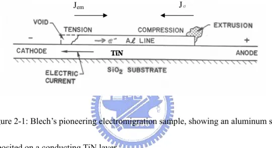
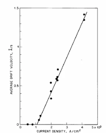
The mass transport of electromigration in a thin metal film can be directly investigated by using the drift velocity method. The method is also called the “saddle movement experiment”. It was first presented by Blech in 1976 and has been widely adopted for the study of atomic drift velocity, activation energy and electromigration parameters. A sample configuration for the drift velocity experiment is shown in figure 2-1. The applied electrical current in the TiN takes a detour to go along aluminum line because the latter is a path of lower resistance. A threshold current density exists and is shown in figure 2-2. Blech found that the threshold current density is approximately inversely proportional to the stripe length, and it is increased by decreasing the temperature or by SiN covering film.
In the past several years, an impetus to study electromigration in very fine conductors has arisen from the development of very large-scale integrated circuits. The conductors are not only interested in small dimensions; they are often assembled into multilayered structure with a certain combination of conductors and insulators. This gives rise to electromigration problems which distinctly different from simple single-level conductor line.
Figure 2-1: Blech’s pioneering electromigration sample, showing an aluminum strip deposited on a conducting TiN layer.
Figure 2-2: Average drift velocity of an aluminum stripe (heat treated 500℃, 1/2h) as a function of current density.
At present, as IC continues to scale down, the bump pitch and diameter also scale down. This leads to current density increase in the solder bumps, thus Electromigration in solder bumps has been recognized to be a new reliability issue in interconnects [18]-[32].
2-2 The Driving Force of Electromigration
Electromigration is the mass transport by the electric field and charge carriers. The driving force of the net atomic flux comes from the applied electrical field and the force has two parts: the first is the direct action of the electrostatic field on the diffusing atoms and the second is the momentum exchange of the moving charge carriers with the diffusing atoms, or the so-called electron wind force.
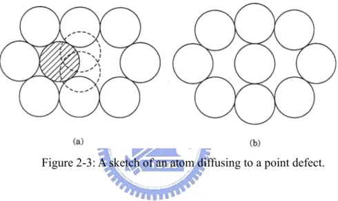
Hungtington and Grone [38] presented a theory to explain electro-migration based on certain simplifying assumptions. It was assumed that (1) the momentum transfer takes place in a conducting metal with a point defect as shown in figure 2-3; (2)Electrons are scattered by the defect alone and the defect is not coupled from the lattice; (3)the scattering occurs without energy lost. Therefore, the momentum transferred to an electron during the scattering process can be expressed as
V m V m V m P= 0∆ = 0 '− 0 ∆ (1) where m0 is the mass of a free electron, V and V’ are the group- velocity of Bloch wave
before and after the scattering. The X-component of the total momentum transferred per unit time is given by
=
∫∫
dt V m d dt dpx ( 0 ) (2) To understand the concept, we express the momentum transportation inmomentum space. Since the group velocity V is equal to k E ∂ ∂ h 1 , the momentum transferred per unit time per unit volume in momentum space as follows
∫∫
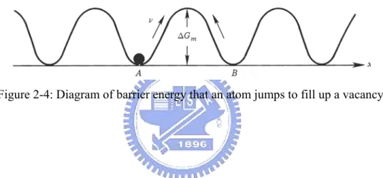
− ∂ ∂ − ∂ ∂ − = f k f k W k k dk dk k E k E m dt dpx ' ' ' ' 0 2 3) ( / )( ) ( )[1 ( )] ( , ) 4 1 ( h π (3)where the function of W(k, k’) gives the transition probability per unit time that the electron in state k jumps to state k’ by virtue of interaction with point defects, in other words, it is the probability that an atom goes over the energy barrier with activation energy ∆Gm as shown in figure 2-4 The f(k) is electron distribution function in
momentum space.
The equation of (3) can be written as
∫∫
− ∂ ∂ − = f k f k W k k dk dk k E m dt dpx ( )[1 ( ') ( , ') ' ' ) / ( ){ 4 1 ( 3 0 h π } ' ) ' , ( )] ' ( 1 )[ ( ) / ( 0∫∫
− ∂ ∂ − f k f k W k k dk dk k E m h (4)by interchanging the primed and unprimed in the first term of equation of (4), the equation becomes
∫∫
− ∂ ∂ = f k f k W k k dk dk k E m dt dpx ' ) ' , ( ) ' ( 1 )[ ( ) / ( ){ 4 1 ( 3 0 h π∫∫
( 0/ ) ( ')[1− ( )] ( ,' ) ' } ∂ ∂ − f k f k W k k dk dk k E m h (5)∫
∫
− − − ∂ ∂ − = f k f k W k k f k f k W k k dk dk k E m / ) { ( )[1 ( ')] ( , ') ( ')[1 ( )] ( ,' )} ' ( ) 4 1 ( 2 0 3 h πEquation of (5) can be simplified by introduction of a relaxation time τd defined by
∫
− − − = − 0( ) { ( )[1 ( ')] ( , ') ( ')[1 ( )] ( ,' )} '/4 3 ) ( π τ f k f k W k k f k f k W k k dk k f k f d (6)Here f0(k) denotes the electron distribution at equilibrium. If the electron distribution
function is normalized to equilibrium state, the substitution of (6) into equation of (5) gives
∫
∂∂ = f k dk k E m dt dp d x ) ( / ) ( ) 4 1 ( π3τ 0 h 0 ( ) /4π3 τ k f k dk E m d∫
∂ ∂ = h (7) The current density in the X-direction jx can be expressed as
∫
∂ ∂ − = ( ) /4π3 dk k E k f e jx h (8) where k E ∂ ∂h is group velocity of Block wave, f(k) is electron distribution function. So the integral represents the total number of electrons per unit time per unit volume in momentum space. By substituting (8) into (7), the momentum exchange can be expressed as d x x e m j dt dp τ 0 − = (9) Since the momentum change is equal to product of force exerted on electrons and period of collision time, namely, ∆p=F∗∆t, the average force for each collision can be
approximated by d x x dtN dp F = d d x N e m j τ 0 − = (10) where Nd is the density of defects. The contribution of the defects to the resistivity is
m
here m* is effective mass of electron, n is density of conducting electrons. So the force can be expressed as function of resistivity ρ as well as electron density n
d d x x m m N nej F =− 0* ρ (12)
in virtue of Ohm Law, x x x j
j ,
ρ ε
= in equation (12) is replaced by electric field and resistivity d x d x m m N ne F ρ ρ ε * 0 − = 0* m m N N z e d d x ρ ρ ε − = (13) where N is density of metallic ions. Z is nominal valence of an ion. The electron density has been replaced by z times the density of metallic ions N. It is worthy to note that Fx
is proportional to three ratios: N/Nd ,the ratio of metallic ions to defects; m0/m*, the ratio
of free to effective electron mass, and ρd/ρ, the ratio of specific resistivity per defect to
per normal atom. The equation of (13) should be modified by a factor of ½ because Fx is
a micro-position function. For example, an ion at the saddle point halfway from an equilibrium site on its way to fill a vacancy (see Fig.2), the interaction with the electrons is strong, whereas at the lattice point the same interaction is a minimum. For simplicity, it is assumed the form of function is a sinusoidal periodicity that contributes a factor of ½, namely, 2 1 * 0 m m N N z e F d d x x ρ ρ ε − = (14) The electron flow might act as a “frictional” force on the metal ions which would
commonly called “electron wind force.” Therefore the total driving forces exert on the moving ion can be given by
wind el field driving F F F = + − * 0 2 1 m m N N z e z e d d x x ρ ρ ε ε − = (15) Let us define the charge number, Zwd, representing the momentum exchange effect
* 0 2 1 m m N N z z d d wd ρ ρ − = (16) The driving force can be presented by the valance of an ion zel and zwd
wd x el x driving e z e z F = ε + ε ) ( el wd x z z e + = ε * z eεx = (17) Generally Zwd has been found to be of the order of ten for a good conductor, so the
momentum exchange effect is much greater than the electrostatic field effect for electromigration in metals.Therefore, the direction of driving force is opposite to electronicstatic field.
2-3 Back stress in electromigration
In early experiments studying electromigration, Blech passed current through aluminum stripes of various lengths deposited on conducting TiN. The schematic diagram of the experiment is shown in figure 2-3. Blech discovered some basic observations in this work [32]-[39]:
3. Below a critical current density, the drift velocity of a given stripe was zero.
The above existences can be explained by atom back flow. Electromigration is short strips can induce back flow, resulting in an atomic flux in the opposite direction. Electromigration pushes atoms towards the anode and builds up compressive stress, leading more vacancies at the cathode side and fewer vacancies at the anode side according to the Nabarro-Herring model. Consequently, there is a gradient of vacancy concentration in the strip, inducing an atomic flux Jσ in the opposite direction to that of
electromigration Jem. When the strip is shorter than a critical length, electromigration
ceases to occur. Base on the above description, equation 2-1 can be rewritten as
dX d KT D C j e Z KT D C X C D J J J J chem em Ω − + ∂ ∂ − = + + = σ * ρ σ (18)
Where σ is the stress and C=1/Ω for pure metal, and Ω is the atomic volume. Jem and
Jσ are the mass fluxes, resulting from electron wind force and back stress respectively.
With no chemical potential gradient along the Al strip, equation can be rewritten as dX d KT D C j e Z KT D C J = * ρ − σΩ (19) there would be no electromigration damage if we assume mass flux J=0 in equation, the critical length △X crit, can be written as below when no electromigration damage occurs
j e Z Xcrit ρ σ * Ω ∆ = ∆ (20) Critical product (j△X)crit can be obtained
(j ρ σ e Z X)crit * Ω ∆ = ∆ (21)
less than the (j△X)crit.
2-4 Electromigration in solder materials
At present, the trend of circuit design, each flip chip solder joint will carry 0.2 A, and to meet the future performance requirement even in a hand-held consumer product, the applied current density will increase. The average current density in a 50 μm solder joint is about 104A/cm2 when 0.2 A current is applied and it will be extended to 0.4 A in the near future. According to the 2000 International Technology of Roadmap for Semiconductors, a current density in the solder bump may reach 1×10⁴ A/cm2 in the near
future. In the device operating temperature range from 80-150℃, electromigration occurs in solder joint and it turns into an emerging reliability issue in microelectronic industry. From the point of view of device reliability, electromigration in a flip chip solder joint is as significant as that in an Al or Cu interconnect line because of the high lattice diffusivity in the solder alloys, higher resistivity, lower Young’s modulus, and higher effective charge number of the chemical elements in solder alloys than those of Al or Cu. It is known that the current density needs to fail a solder joint is about two orders of magnitude less than that needed to fail an Al or Cu line. Besides, due to the unique geometry of a flip chip configuration, current crowding effect takes place at the contact interface between conducting metal line and solder bump, a high Joule heating generates simultaneously and accelerates solder bump to failure [18] [40].
In 1976, Sun and Ohring devised a nondestructive technique to study lateral self-diffusion and electromigration in evaporated thin Sn film [49]. The diffusional spreading and migration of tracer distributions of Sn119m in thin Sn film matrices was
recorded over a temperature range 142-213℃ . They found out the diffusivity D
(
1.8 1.9)
10 5exp( 10700 700 ) 2/sec 9 . 0 × − ± RT cm = + −− and migration velocity V =(1.07 1.10) 10 4/ exp( 9800 650/ ) /sec
54 .
0 × − T − ± RT cm +
− at a current density of 1×10⁴A/cm2. The effective charge Z* and defect resistivity were also derived. The results are consisted
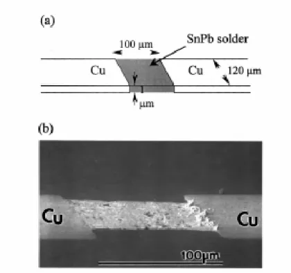
with a bulk-assisted grain boundary transport mechanism involving a vacancy defect. Liu et al. studied a thin stripe of eutectic SnPb solder stressed by a current density of 105 A/cm2 at room temperature [20]. The test sample was prepared by a Cu/Cr thin film deposited onto an oxidized Si substrate by a process of e-beam evaporation. By using lithographic and etching method, two thin film lines of 120 μm width and 1 μm thickness, with a separation of 100 μm, were patterned on the SiO2/Si substrate, as
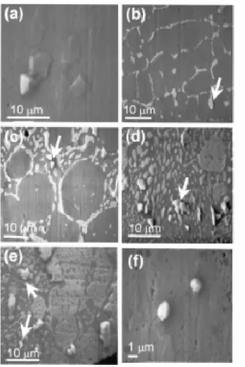
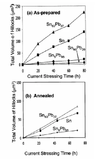
depicted in figure 2-5 (a). Figure 2-5 (b) illustrates the scanning electron microscopic (SEM) image of a eutectic SnPb solder stripe after it was stressed by a direct electrical current density of 105 A/cm2 at room temperature for 19 days. Hillocks are observed in the anode side near the interface between the solder and Cu. They also discovered that the dominant diffusion species is Sn in the SnPb alloy, and the growth of the hillocks originates from the Pb grain. Later, they investigated the electromigration of six different compositions of Sn-Pb solders. The eutectic alloy with the lowest melting point and a high density of lamella interface was found to have the fastest hillock growth, as shown in figure 2-6. The results also indicated that the annealed samples with a larger grain size showed a slower hillock growth rate, as shown in figure 2-7.
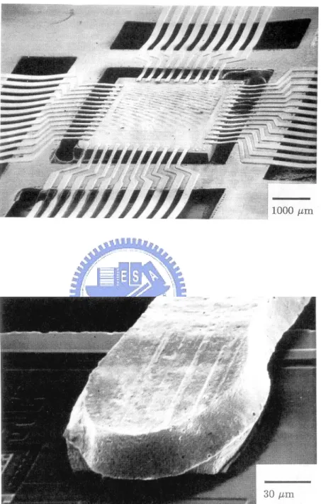
schematic diagrams of a V groove on and the cross section of a V groove are shown in figure 2-8. Figure 2-9 shows the SEM images of microstructural evolution of the test sample. The sample was stressed by a current density of 2.8×10⁴ A/cm2 at 150℃ in
ambient. They measured the volume of the lump, and calculated the average effective charge number of electromigration in eutectic solder is 33, which is close to the value of 47 for self-electromigration in bulk Pb.
Yeh et al. investigated electromigration failure in flip chip solder joints [27], they discovered that at the contact interface between the bump and the wire, a very large current crowding occurs and it causes a unique and fast electromigration failure in the bump. The schematic illustration of a flip chip solder joint and its simulation are respectively shown in figure 2-10 (a) and (b).
Lee et al. studied the electromigration of eutectic SnPb solder interconnects between a Si chip and a FR4 substrate at 120℃. Hillocks were observed at the anode and voids at the cathode [24]. The dominant diffusing species was found to be Pb. In addition, they use the surface marker to measure the electromigration flux and calculate the effective charge in the SnPb solder joint.
Figure 2-5: (a) Schematic picture of the eutectic SnPb solder thin stripe sample. (b) The SEM image of an solder stripe after stressing
Figure 2-6: Hillock formation of as-prepared Sn-Pb alloys after 40 h current stressing at ambient temperature: (a) pure Sn; (b) Sn80Pb20; (c) Sn70Pb30; (d) eutectic SnPb; (e) Sn40Pb60; (f) Sn5Pb95.
Figure 2-7: Total volume of hillock vs the current stressing time: (a) as-prepared, and (b) annealed
Fig 2-8: Schematic diagram of (a) A V groove on (001) Si surface with two Cu wires as electrode at the two ends and (b) the cross section of a V groove and its dimensions.
Figure 2-9: SEM images of the surface of a eutectic SnPb wire on V groove of 100 μm wide and 150 μm long stressed by 2.8×10⁵ A/cm2 at 150°C in ambient. (a) Before
electromigration, (b) after four days, (c) after eight days, and (d) same as the sample shown in (c) except that a layer of 10 mm has been polished away from the surface
Figure 2-10: (a) A schematic illustration of a flip chip solder bump. (b) The simulated current distribution in the solder bump.
Figure 2-11: The marker movement on the cross-sectioned eutectic SnPb surface. (a) Marker on the cross-sectioned surface. (b) marker displacement.
(a)
2-5 Motivation of this study
Several studies have addressed the electromigration issue of SnAgCu alloy [24] [41] -[46].Choi et al. measured the mean-time-to-failure (MTTF) of eutectic SnAgCu bumps, and they attempted to determine the effective charge number (Z*) of the solder by marker movement. But the marker movement was too small to be measured. Lin et al. investigated the current carrying capability of eutectic SnAgCu bumps, and found that there was no electromigration damage in the bumps after stressing by 2.5 × 10⁴ A/cm2 at
150 °C for 2338 hours. However, the relevant parameters of electromigration, such as threshold current density (Jc), drift velocity, activation energy (Ea), and the product of diffusivity and the effective charge number (DZ*) of the eutectic SnAgCu solder are still unknown.
This lack of information is because of the difficulty in preparing Blech-type electromigration test specimens of SnAgCu solder. Blech developed a unique set of test structures of short stripes of Al on a TiN base line for the measurement of the drift velocity of electromigration so that the relevant parameters of electromigration can be determined [39] [47]. However, eutectic SnAgCu solder stripes have not been deposited by evaporation, sputtering, or electroplating. In addition, the solder is very soft, and it is hard to pattern it into short stripes. In this study, we report a process to fabricate solders Blech specimens, and we employed atomic force microscopy (AFM) to measure the depletion volume and drift velocity on the cathode side. As a result, we obtained direct and precise measurement of the solder electromigration parameters. Besides, electromigration in SnAgCu solder was carried out by the flip chip solder joint, the
failure mechanism due to electromigration will be discussed in this study as well. In addition, the electromigration in flip-chip SnAgCu solder joint was also studied. The electromigration behavior in the solder bumps was investigated at 100℃and 150℃.
Chapter 3: Electromigration Study in Pb-free SnAg
3.8Cu
0.7Solder joints
with Ti/Cr-Cu/Cu Under-Bump Metallization
3-1 Sample preparation and experimental procedures
A UBM of a Ti/Cr-Cu/Cu tri-layer was deposited on the chip side, and a Cu/Ni(P)/Au pad was electroless plated on the BT board side. The solder bumps on the chip were formed by printing solder paste through a metal stencil and were reflowed in a furnace at 250℃. The chips are then flipped over, aligned to BT substrates, and reflowed again. The reflow profile for the solder bumps is presented in Fig.3-1. Afterwards, the package was filled with underfill. The solder bumps were electrically connected by an Al line in the chip, while Cu line was used in the BT board side. A schematic illustration of the structure is shown in Fig. 3-2(a), which shows that the contact window in the chip side was 85μm and 150μm for board side. The pitch for the sample was 400μm. Figure 3-2(b) is a three-dimensional schematic diagram of the bump pairs subjected to electromigration testing in which the routes for electrical current are depicted. Two sets of bump pairs, Pair A and Pair B were employed for electromigration study. The current paths for bump Pair A and Pair B are indicated by the arrows in Fig. 3-2(b).
Cross-sectioned bumps and whole-bump samples were prepared for the electromigration test. Cross-sectioned bumps refer to those bumps which had been cross-sectioned first and then stressed. To investigate current crowding effect, two different cross-sections, i.e. cross-section A and cross-section B were prepared, as shown schematically in Fig. 3-2(c). The samples were stressed at 100℃ or 150℃on a hot plate in an ordinary atmospheric conditions. The calculated current density was 2 × 10⁴
A/cm2 for contact opening on the chip side and 6.6 × 10³ A/cm2 for the contact opening
on the board side. Resistance change caused by electromigration was monitored every ten second during the current stressing. Electromigration damage was examined using a
Figure 3-2: (a) Schematic cross-sectional view of a pair of solder bumps. (b) Schematic three-dimensional view of the position of conducting lines related to the bumps, (1) Pair A, (2) Pair B. (c) Schematic three-dimensional view of a solder bump, defining cross-section plane A and cross-section plane B used in this study.
(a)
(b)
to determine the composition of intermetallic compounds (IMCs) and distribution of metal atoms.
3-2 Results
A. Composition and Microstructure of the Intermetallic Compound (IMCs) before Current Stresssing
Fig. 3-3(a) illustrates the cross-sectional SEM image of the SnAgCu solder bump before current stressing. In the bulk solder, the composition of the IMC was identified to be Cu6Sn5 with dissolution of 2-4 atomic percent of Ni. The Ag3Sn particles were
also found in the solder bump. Figs. 3-3 (b) and 3-3(c) show the enlarged SEM images of the chip side and the BT board side respectively. A layer of IMC with thickness of 0.7μm was formed between the solder and UBM interface at the chip side. On the BT board side, IMC of Cu6Sn5 with dissolution of 15-20 atomic percent of Ni was observed.
B. Electromigration in cross-sectioned solder bump
Figure 3-4(a)-(d) shows the microstructure evolution in the cross-sectioned SnAgCu bump before and after stressing by the current of 0.085 ampere for 20 h, 264 h, and 408 h at 100℃ respectively. The bump was polished in cross-section plane A before stressing, and the remaining cross-section area on the chip side was measured by the cross-sectional UBM length. Thus, the current density for the bump can be obtained. The current density used to stress the cross-sectioned bump is 2× 10⁴ A/cm2. The direction of
electron flow is from the chip side to the board side, as shown in the left bump of pair A in Fig. 3-2(b). Voids formed at the solder and UBM interface after reflow can be seen in Fig. 3-4(a). After stressing for 20 hours, a hillock was observed at the chip side as
Figure 3-3: Cross-sectional SEM images of a solder bump before current stressing. (a) whole bump view, (b) enlarged image on the chip side, (c) enlarged image on the board side.
Figure 3-4: Cross-sectional SEM images of solder bump stressed at 100℃ for (a) 0 h, (b) 20 h, (c) 264 h, (d) 408 h.
indicated by the arrow in Fig. 3-4(b). From EDS analysis, this hillock contained both Sn and Al. As shown in the left bump in Fig. 3-2(b), the electrons enter the bump from the back-left corner of the UBM on the chip side, migrate both Al and Sn atoms to form the hillock. After stressing for 264 hours, no further damage was observed as shown in Fig. 3-4(c). However, after 408 h of stressing, the solder bump failed. In the upper-left corner of the bump in fig. 3-4(d), a large void was observed, which may be responsible for the failure of the Pair A bump. Fig. 3-5(a) shows the enlarged SEM images of the rectangular area in fig. 3-4(d). The surface of the void appears to be very smooth; from which it may be inferred that the vicinity underwent a liquid state before failure occurred. Furthermore, some tiny solder balls were found on the surface near the void, which implies that the local temperature in the void may surpass the melting point of the solder at the moment of failure. Figs. 3-5(b) shows the corresponding X-ray mapping for Al and Ti atoms,respectively. The migration of Al atoms can be clearly seen in these 2 figures.
To examine the polarity effect, the current direction was reversed for the other bump of pair A, i.e. the direction of electron flow goes from board side to the chip side. Figure 3-6(a) - (d) shows the microstructure evolution before and after current stressing for 20 h, 264h , and 408 h at 100℃ respectively. The Al was squeezed out at the chip/anode side after stressing. Figure 3-7(a) and (b) show the enlarged SEM images of the damage and the corresponding X-ray mapping for Al, at the interfacial region. On the board side, no obvious electromigration damage was found for the preceding two bumps. This may be attributed to the lower current density on the board side.
Figure 3-5: (a)Enlarged SEM image of the rectangular area in Fig. 4(d), and corresponding X-ray mapping of (b) Al.
Figure 3-6: Cross-sectional SEM images of solder bump stressed at 100℃ for (a) 0 h, (b) 20 h, (c) 264 h, (d) 408 h.
Figure 3-7: (a) Magnified SEM image of the rectangular area in Fig. 6(d) and (b) is the x-ray elemental mapping for Al at interfacial region in (a).
C. Electromigration in Whole Bump
In Pair B case, the set of whole bumps were stressed at the current density of 1 × 10⁴
A/cm2 until failure occurred. Afterwards, they were subject to cross-sectioning for failure analysis. Figure 3-8(a) shows the cross sectional SEM images of the solder bump along cross-section plane A. The bump failed after stressing for 140 h at 100℃, and was then ground, cut, and polished away approximately 1/3 volume of the solder bump. The Cu-Sn intermetallic compounds were accumulated at the anode/board side, which implies that the Copper atoms on the chip side and in the solder were caused to migrate by the electron flow to the board side.
To examine the microstructure beneath the cross-sectioned surface in figure 3-8(a), further polishing was performed. Figure 3-8(b) and (c) shows the microstructures after polishing away half the volume and two-thirds the volume of the solder bump. Comparing both figures, crack appears to be larger as the bump was polished down.
Fig. 3-9 shows the cross-sectional SEM image of the solder bump along the cross-sectioned plane B. Solder bump failed after 42 h of current stressing at 150℃. Because the test temperature was raised up to 150℃, the failure time decreased from 140 hours at 100℃ to 42 hours. Obviously, the voids at the right are much bigger than the ones on the left as the result of the current crowding effect.
Figure 3-8: Cross-sectional SEM image of the solder bump stressed at 100 ℃ for 140 hours, (a) after polishing to one-third of the bump volume, (b) after polishing half of the bump volume, (c) after polishing two-thirds of the bump volume.
Figure 3-9: Cross-sectional SEM image of the solder bump stressed at 150℃ for 42 hours.
3-3 Discussion
A. Current Crowding Effect on Bump Failure
In the case of the cross-sectioned bump, the solder bump failed after 408 hours of current stressing, as shown in Fig. 3-4(a) through (d). The corresponding schematic picture of the bump is shown in the left bump of pair A in Fig. 3-2(b), where the electrons crowded into the bump from the upper-left-back corner. At the early stage of current stressing, it was speculated that atoms around the corner were migrated to the board/anode side, and voids started to form at the point where current crowding occurred. As voids aggregated to form cracks, the contact area on the chip side decreased, forming a vicious cycle and deteriorated the contact. As the cracks move toward the cross-sectioned surface, current density increased dramatically, heating up the bump locally because of Joule heating. It is believed that the local temperature at the failure site was ramped over the melting point of the solder before failure because there were tiny solder balls observed near the voids. Furthermore, the surface morphology of the void has a smooth appearance which also implies that the solder may have been in a molten state before the failure.
In Fig. 3-9, voids at the upper-right corner are much bigger than those at the upper-left corner. This may be the result of current crowding, where the electrons crowded into the bump from the upper-right corner of the bump. At the board side in Fig. 3-9, Cu-Ni-Sn IMC grew thicker at the lower-right corner, which was attributed by the current crowding on the board side.
The results for the measured resistance of the stressing circuit as a function of
stressing time is shown in Fig. 3-10. Although the resistance included both the resistance of the conduction lines and that of the bump pair, it was still observed that the failure time depended on the dramatic increase of the resistance. As expected, the bump failed within 42 hours of stressing time at 150℃, and within 142 hours at 100℃ because the diffusivity of metal atoms are larger at high temperature. To examine the microstructure changes caused by thermal effect, reference bumps were employed to undergo the similar thermal history during current stressing. Figure 3-11 shows the microstructure changes resulting from the thermal effect only. The bump was kept at 150℃ for 42 hours, and no obvious microstructure change was observed .
C. Interface Analysis after Current Stressing
An enlarged image of the chip side of the bump in Fig. 3-8(c) is shown in fig. 3-12. The crack was found at the solder/IMC interface. Above the crack, the EDS composition analysis at point 1 and point 2 indicated that there are Al, Ti, Cr, Cu and Sn in this region. It is believed that Al, Ti, and Cr atoms migrated by the electron flow into IMC. Because Cu atoms were caused by the electron flow to migrate toward the board side to form a Sn-Cu compound, the analysis at point 3 and point 4 revealed that only Sn and Ag atoms were detected at this region. The composition of these points in the solder is shown in table 3-1.
Figure 3-10: Measured resistance of the stressing circuit as a function of stressing time.
Figure 3-11: Cross-sectional SEM image of the reference bump, the bump was kept at 150℃ for 42 hours.
3-4 Conclusions
The electromigration-induced failures in SnAg3.8Cu0.7 solder joints on Ti/Cr-Cu/Cu has been investigated under current density of 1 × 10⁴ A/cm2 and 2 × 10⁴
A/cm2 at 100℃ and 150℃. The bumps failed at chip/cathode side. Cracks occurred along the solder and UBM interface, which led to the open failure of the bump. The current crowding effect played an important role on the failure. However, the electron flow does not cause apparent damage at the board side because of a much lower current density there than that in the chip side.
Chapter 4: Electromigration in Pb-free SnAg
3.8Cu
0.7Solder Stripes
4-1 Sample preparation and experimental procedures
A similar process to fabricate Blech’s specimens of Al stripe is adopted to fabricate the solder specimens. The main difference here is that the solder Blech specimen was fabricated in a Si trench, in which the top Si surface served as a polishing stopper during the subsequent polishing process. A four-inch p-type Si wafer was cleaned by piranha solution (H2O2 and H2SO4 at the ratio of 1:7) for 10 minutes at 100℃. After cleaning, the
silicon wafer was patterned by photolithography and deep reactive ion etching (DRIE) to form dumbbell-shaped trenches of 3.1 µm in depth. Then, a 1200 Å SiO2 insulating layer
was grown on the wafer. Subsequently, titanium and copper films with thicknesses of 1700Å and 4000Å, respectively, were thermally evaporated onto the silicon wafer by an e-beam evaporator. Thereafter, the copper film inside the trench was patterned and selectively etched to form a short stripe, and two pads were also patterned on the Ti film, which served as a wetting metallization layer for the SnAgCu solder during the subsequent reflow process. Then the wafer was cut into small pieces, with a die in each piece. Solder paste of SnAg3.8Cu0.7 was applied to the Cu stripe at 230℃ for 2 seconds,
in which the subscripts in SnAg3.8Cu0.7 stand for weight percent. After the reflow process,
the thickness of the solder may be over 10 µm thick, and its shape was bump-like. Therefore, a polishing procedure was needed to thin down the solder stripe. The thickness of the solder stripe was controlled by the thickness of the Si trench, since the top Si surface served as a polishing stop for the solder stripe.
Figures 4-1(a) and (b) illustrate the schematic diagrams of the tilted and cross-sectional views of the specimen, respectively. The two square pads at the two sides of the specimen were the electrodes, and the central solder stripe was the specimen to be studied. The stripe was 350 µm long and 80 µm wide. A layer of Cu6Sn5 intermetallic
compound (IMC) grew between the Cu and the solder during the reflow, as shown in Figure 4-1(b). The thickness of the solder was about 1 to 2µm, and it varied from sample to sample due to the polishing process, which polished some of the Si stopper. The samples were then stressed at various current densities and temperatures, and the direction of the electron flow is indicated by the arrows in Figure 4-1(a) and 4-1(b).
Transmission electron microscopy (TEM) and scanning electron microscopy (SEM) were employed to observe the microstructure of the solder stripes. Focused ion beam (FIB) was utilized to prepare cross-sectional TEM specimens. AFM was used to measure the depletion volume on the cathode side of the samples. Each specimen was scanned in AFM six times in order to measure the volume before and after the current stressing, the standard deviation was less than 1% compared with the average volume.
The temperature increment due to the Joule heating effect was monitored by an infrared microscope, which has 0.1℃ temperature resolution and 2µm spatial resolution.
4-2 Results
A. Microstructure of the SnAgCu stripe and temperature measurement
Figure 4-2(a) demonstrates the backscattered electron (BSE) SEM image of the fabricated solder stripe, formed inside the Si trench. Figure 4-2(b) is the enlarged (BSE) SEM image for one end of the stripe. Typically, the four corners of the Cu stripe could
Figure 4-1: (a) Tilted-view schematic of the solder stripe on a Ti film in a Si trench. (b) Cross-sectional schematic of the solder Blech specimen. The direction
(a)
e
SolderTi
Silicon(b)
e
SiO2 Ti Cu6Sn5 Silicon SnAgCuFigure 4-2: (a) BSE SEM image of the fabricated dumbbell-shaped stripe. (b) Enlarged SEM image for one end of the stripe
Pad
Pad
Si substrate
Solder stripe
100µm
(b)
not be wetted by molten solder paste during sample preparation. Figure 4-3(a) illustrates the cross-sectional TEM image of the specimen. A layer of scalloped Cu6Sn5 intermetallic
compound (IMC) is formed between the SnAg3.8Cu0.7 solder and the Cu layer. The SiO2
and Ti layers can be clearly seen in the figure. The Cu film was consumed almost completely, but a few small Cu islands may be observed under some large IMCs. Since the Cu layer is not continuous, it is not considered when calculating the effective current density in the solder stripe. Figure 4-3(b) displays the enlarged cross-sectional TEM image of the area within the white circle in figure 4-3(a). The grain size was about 1 µm in diameter. We speculate that the minuscule grain size was due to the film thickness and the rapid cooling rate in the sample preparation process. Through theoretical calculations, it was found that about 80% of the applied current would flow inside the solder, whereas about 19% of the current drifted along the IMC layer, and only about 1% stayed in the Ti layer.
Figure 4-4 displays the temperature increment in the solder stripe as a function of current density at 80°C, 100°C, and 120°C measured by a infrared microscope. The highest temperature increment was merely 5°C when the specimen was stressed by 0.12 A, which corresponded approximately to 1×10⁵ A/cm2 in the solder stripes. The Joule
heating effect in the stripes was much lower than that in the flip-chip solder bump [48]. This effect may be attributed to the stripe geometry and the excellent heat conduction of silicon substrate.
B. Threshold current density of the SnAg3.8Cu0.7 solder
![Table 1-1 Chemical composition of 79 lead-free solder alloys down-selected for preliminary testing by the National Center for Manufacturing Science (NCMS) [16]](https://thumb-ap.123doks.com/thumbv2/9libinfo/8748135.205338/26.892.221.688.257.992/chemical-composition-selected-preliminary-testing-national-manufacturing-science.webp)
![Table 1-2 Criteria for bown-selection of Pb-free solder alloys [16].](https://thumb-ap.123doks.com/thumbv2/9libinfo/8748135.205338/27.892.247.669.393.886/table-criteria-bown-selection-pb-free-solder-alloys.webp)