國
立
交
通
大
學
電控工程研究所
碩
士
論
文
量化器超載模型與模組設計最佳化運用
在離散時間積分三角類比數位轉換器
Quantizer Overload Model and Model-based Design Optimization for
Discrete-Time Sigma-Delta Modulators
研 究 生:歐嘉昌
指導教授:陳福川 教授
量化器超載模型運用於模組化設計離散
時間積分三角類比數位轉換器
Quantizer Overload Model and Model-based Design Optimization for
Sigma-Delta Modulators
研 究 生:歐嘉昌 Student:Chia-Chang Ou
指導教授:陳福川 Advisor:Fu-Chuang Chen
國 立 交 通 大 學
電 控 工 程 研 究 所
碩 士 論 文
A ThesisSubmitted to Department of Electrical and Control Engineering College of Electrical Engineering and Computer Science
National Chiao Tung University in partial Fulfillment of the Requirements
for the Degree of Master
in
Electrical and Control Engineering September2010
Hsinchu, Taiwan, Republic of China
量化器超載模型運用於模組化設計離散
時間積分三角類比數位轉換器
研究生:歐嘉昌 指導教授:陳福川 教授 國立交通大學 電控工程研究所摘要
摘要: 在離散時間積分三角調變器規格設計上,通常都依賴模擬化設計方法。然而,由於在 模擬化設計中會需要進行積分三角調變器的行為模擬,因此如果使用模擬化方法去設 計積分三角調變器則十分的耗時。然而使用演算法去降低資料的數量,存在著結果可 能不夠理想的風險。本論文中,我們提出模組化積分三角調變器最佳化設計方法。此 方法可以在極短時間之內計算出積分三角調變器所需要的規格,使得積分三角調變器 可以得到最小的功率消耗以及最大的訊號對雜訊和失真比例。而且因為模組化設計方 法非常的省時,因此在做積分三角調變器最佳化當中,不需要使用演算法去降低計算 量。不過,使用模組化積分三角調變器最佳化設計上,會出現量化器超載問題;此問 題我們將在之後的章節進行討論。此外,本論文還會提出一個數位類比電路失真模型。 最後將針對兩個已發表的設計範例去驗證模組化積分三角調變器設計的可行性。Quantizer Overload Model and Model-based Design Optimization for
Sigma-Delta Modulators
Student:Chia-Chang Ou Advisor:Dr. Fu-Chuang Chen
Institute of Electrical and Control Engineering Nation Chiao Tung University
ABSTRACT
The conventional high-level SDM synthesis is mainly based on behavior simulation which is very time-consuming. This paper is the first one in the literature to propose model-based SDM synthesis. Model-based approach can be at the order of 104 times faster than simulation-based approach, but it is never realized before due to the incompleteness of non-ideality models. The recent establishment of settling noise model and OTA distortion model facilitates model-based SDM designs. Nonetheless, new problems associated with model-based approaches arise, notably overload on quantizers. In this paper, a SDM input estimator is proposed to avoid quantizer overload. In addition, a SDM design optimization scheme is proposed, which incorporates a DAC distortion model. Either the DAC distortion model is used, or data weighting average (DWA) power is estimated. This model-based optimization is tested against two published SDM designs, achieving higher SNDR and lower power results in a much shorter design time.
誌謝 Acknowledgment
我要將此論文獻給 我親愛的母親-李淑美 女士 最疼我的父親-歐聰榮 先生 若沒有他們,我不可能有機會完成此篇論文,並且從交通大學碩士班畢業。此外, 必須感謝指導教授陳福川博士兩年來嚴格的督促與指導,讓我學會做研究的方法與心 態,以及英文程度上的提升。另外,也要感謝口試委員廖德誠教授、洪浩喬教授與趙 昌博教授對本篇論文所給予的建議與指導。 還要感謝實驗室智龍、瑞祺、武璋學長在我一年級時幫我打好深厚的研究基礎。 感謝實驗室同學子恩和學弟國政、瑋才、揚程陪我度過最後的學生生涯,並在研究上 給予我很多幫助。最後要謝謝這兩年在新竹唸書期間所有幫助過我的人,雖然無法一 一列舉,但在這邊向大家致上最大的謝意。Contents
中文摘要 ... I English Abstract... II Acknowledgment... III Contents ...IV Lists of Tables ...VI Lists of Figures ...VII List of Symbols ...VIII
Chapter1 Introduction...1
1.1 Background, Current Status, Motivation and Aims ... 1
1.2 Organization ...3
Chapter2 Discuss About Non-idealities Noise and Distortion Models of 2nd Order Single Loop SDM and MASH SDM...4
2.1 SDM Noise Power and Distortion power models... 5
2.2 DAC Nonlinear Distortion Power Model... 9
2.3 Non-idealities Models for MASH SDM Architecture...14
2.4 Non-idealities Models for Other Architecture………...15
Chapter3 New Problems Associated to Model-Based Designs... 17
3.1 Identifying Essential Non-idealities Models for Model-Based Designs...18
3.2 Quantizer Overload Problem... 19
Chapter4 Two Examples for High-Level Synthesis of DT SDM Based On Model-Based Designs ... 24
4.1 Design Optimization Schemes ... 24
Chapter5 Conclusion ... 26 Appendix... 27 A.1 an Approach for Extracting Sine Wave Signal from Any Order SDM Output
(Behavior Simulation)... 28 A.2 Error Function ... 28 References ... 29
Lists of Tables
Table 2.1 Important SDM design parameters ... 5 Table 2.2 Simulation results for various σdac and u combinations with Ain=0.5v ... 13
Table 2.3 Theoretical results and simulation results for various and u combinations
with Ain=0.7v ... 14
dac
σ
Table 3.1 Simulation results and theoretical results for various B ... 22 Table 4.1 Comparisons of our design results with those in [34] ... 28
Lists of Figures
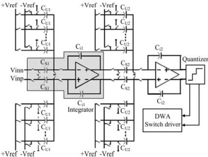
Fig. 2.1 Circuit topology of 2nd order single loop SC SDM... 4
Fig. 2.2 A block diagram of a B-bit flash DAC ... 9
Fig. 2.3 DAC transfer curve: (a) DAC with smaller DAC output error, and (b) DAC with larger DAC output error... 10
Fig. 2.4 DAC transfer curve: (a) DAC with fewer output levels, and (b) DAC with more output levels ... 11
Fig. 2.5 Behavior simulation for DAC nonlinearity ... 13
Fig. 2.6 2-1 Mash architecture of SDM ... 14
Fig. 3.1 The performance of SNDR versus SDM input signal amplitude. ... 18
Fig. 3.2 The block diagram of 2nd-order single-loop SDM ... 19
1( ) q f x The pdf of q1(n) (b) q ( ) 2 f y The pdf of q2(n) ... 21 Fig. 3.3 (a) Fig. 3.4 (a) The theoretical pdf of q(n) (b) The simulated distribution of q(n)... 21
List of Symbols
Symbols
VLSB OS V OSR n B fS fB Vref A0 fin Ain . jit σ CS CI VS T Ron . cap σ K Erf SR GBW h Vov fcr . capε
CU a1 V2nOTA a a −Quantizer step size
Maximum output swing of op-amp Oversampling ratio
Order of the Sigma-Delta modulator Number of bits in the quantizer Sampling frequency
Signal bandwidth
Reference voltage of the quantizer Finite gain of OTA
Frequency of the input signal Amplitude of input signal
Standard deviation of clock jitter Sampling capacitor
Integrating capacitor
Input signal plus feedback DAC signal Absolute temperature
Switch on resistance
Standard deviation of mismatch of unit capacitance Boltzmann’s constant (1.38×10⁻²³) J/K
Error Function Op-amp slew-rate Op-amp gain bandwidth Comparator hysteresis Overdrive voltage Corner frequency
Capacitor mismatch error Unit DAC capacitor
The gain of first stage integrator in 2nd order SDM Input-referred PSD of OTA
The value of activated unit DAC The value of deactivated unit DAC
ek -ek μ σ VSW Ceq
Activated mismatch error of unit DAC Deactivated mismatch error of unit DAC Finite dc-gain error
Standard deviation
Swing of quantizer input node Equivalent capacitor of integrator
1
Introduction
1.1 Background, Current Status, Motivation and Aims
Sigma-Delta modulator (SDM) A/D converter is the most popular topology for high resolution applications because the SDM is implemented by feeding back quantization signal which reduces the quantization noise power [1]. Besides, the SDM is essential for system-on-chip (SoC) design, due to smaller area and lower power consumption [2]. The SDM can be implemented by continuous-time (CT) or discrete-time (DT). DT SDM with switch-capacitor (SC) implementation is much more popular than CT SDM because CT SDM suffers from problems such as sensitivity of clock jitter and excess loop delay [3]. We will focus on the design of SC SDM in this research.
In SDM designs, the designer needs to adjust design parameters so that high SNR or SNDR [4] can be achieved. The design parameters include oversampling ratio (OSR), sampling capacitor, op-amp gain bandwidth, op-amp slew-rate, op-amp DC-gain, quantizer bit number, etc. The variation of any single design parameter can potentially affect several noises and distortions in different ways, and may change system power consumption. For example, increasing OSR can reduce quantization noise, but increases settling noise and power consumption. It is typically a complex task to adjust all design parameters to come up with a good design. Currently, the design tasks rely heavily on simulation tools. Conventional circuit simulator (SPICE) provides high accuracy, but it takes too long simulation time. In order to overcome this problem, various SDM simulators have been developed such as circuit-based macro models [5], time-domain macro models [6], finite difference equation [7], table-lookup models [8] and behavior simulation technique [9], [10]. The circuit-based macro models are equivalent circuits made from components available in the circuit simulator. It increases the
speed over circuit simulator but still needs too much time for simulation. The time-domain macro models are based on the time-domain equations used to describe the circuit transient behavior. Although it produces quick simulation and can model dynamic error, this approach is not flexible. The finite difference equations model is based on the z-transfer function of SDM. It produces the quickest simulation time. However, the capability for modeling non-idealities is poor. The table-lookup model is quick, but not flexible [11], [12]. Recently, behavior simulation technique provides good accuracy, high speed and more flexibility [2], [11]. In the early period, the behavior simulator used event-driven behavior simulation techniques [13]-[15]. In these techniques, the behavior simulators are implemented in C-language. Therefore, the block models can’t be easily modified [2]. Recently, in order to overcome this problem, the most popular approach is to implements the behavior simulation in MATLAB Simulink environment [2], [3], [16]-[18]. On the other hand, there exist behavior simulations by using VHDL-AMS and Verilog-A [19]-[23]. The VHDL-AMS behavior simulation provides faster simulation time than MATLAB Simulink [23] and the Verilog-A behavior simulation can provide many choices between accuracy and efficiency [22]; however, to date, both simulations are not popular enough for SDM designs. Since behavior simulation is very time consuming, in order to search for adequate design parameter combinations at much lesser cost, recently techniques related to simulated annealing [2] and generic algorithm [14], [24] have been employed. However, the designs obtained in such cases are suboptimal.
This thesis is the first one in the literature to propose model-based SDM design method. In contrast to simulation-based designs reviewed above, model-based designs can potentially be at the order of 104 times faster. Model-based designs can also explicitly compute each noise
power and distortion power, greatly enhancing design process, while simulation-based designs only generates sum of noise and distortion powers.
Model-based designs require that all relevant noise models and distortion models be available. During the past two decades, most non-ideality models have been developed [4, 13,
27, 28, 29], except that models for op-amp nonlinear DC-gain distortion and settling noise were critically lacking. This is the reason model-based SDM design has never materialized. Recently, however, both the nonlinear DC-gain distortion power model and the settling noise power model have been proposed in [25] and [26] respectively. Thus model-based design becomes possible. Nonetheless, new problems associated with model-based design surface, notably the overload problem.
The overload issue is due to quantizer overload may seriously degrades SDM performance. In this research, we establish model to estimate maximum SDM input signal allowed such that quantizer overload problem can be avoided. A model-based design optimization algorithm is also proposed, which is applied to a previously published SDM design task to demonstrate capability and advantage of model-based design method. The model can significantly improve model-based SDM designs.
1.2 Organization
The rest of chapters are organized as follows. Chapter 2 describes all non-idealities noise and distortion power models of 2nd order single loop SDM and MASH SDM. Chapter 3 presents the new problems associated to model-based designs. Chapter 4 presents the design optimization scheme and two examples for high-level synthesis of DT SDM based on model-based design. Chapter 5 presents the conclusion of this thesis.
2
Discussion about Non-idealities Noise and
Distortion Models of 2
nd
Order Single Loop
SDM and MASH SDM
Model-based high-level SDM designs employ only mathematical models. In this chapter, we will first check about the availability of noise and distortion models against all non-idealities in SDM, which are functions of design parameters. Important design parameters are listed in TABLE 2.1. Modification to existing models will be made wherever needed. We will propose a DAC distortion power model since no DAC distortion model is available up to date. The models discussed in this section are for the popular single-loop two-stage SDM structure shown in Fig. 2.1. Models for MASH and other SDM structures are also discussed in the rest of section of this chapter.
TABLE 2.1
Important SDM design parameters
Symbol Design parameters Symbol Design parameters
B bit number Vov overdrive voltage
OSR oversampling ratio Vref quantizer reference voltage
GBW op-amp gain bandwidth fcr corner frequency
SR op-amp slew-rate Ron switch on resisance
CS first stage integrator sample
capacitance
εcap capacitor mismatch error
Ain input signal amplitude fB input signal frequency
A0 op-amp DC-gain Vos op-amp output swing
σj sampling uncertainty Ci first stage integrator integral
capacitance
h comparator hysteresis σdac standard deviation of DAC capacitor
mismatch error
2.1 SDM Noise Power and Distortion Power Models
For the 2nd-order switch capacitor SDM shown in Fig. 2.1, major circuit non-idealities are listed below:
1) Switches non-idealities; 2) Capacitors non-idealities; 3) Finite and nonlinear DC-gain; 4) Bandwidth and slew rate; 5) OTA noises;
6) Clock jitter effect; 7) Comparators;
8) Multi-bit DAC non-idealities.
outside of integrators. In the following, noises and distortions power models related to each of eight nonidealities are discussed.
1) Switch Non-idealities
y Switch thermal noise power model (PSwitch_thermal) [4, 13]. PSwitch_thermal from switches
before CU and CS. The Power Spectrum Density (PSD) of switch thermal noise at SDM
output is derived as 8KT/CS. Therefore, the in-band switch thermal noise power is
B B S S f Switch_thermal -f 8KT 1 8KT C OSR C P =
∫
df= (2.1)y Nonlinear switch resistance distortion power model (PSwitch_distortion) [4]. The switch
on-resistance is nonlinear because its value depends on input signal. The related SDM output distortion power PSwitch_distortion can be obtained from [27].
y Clock-feedthrough. The clock-feedthrough is caused by the charge of the gate-to-source capacitors of the switch that is injected to the sampling capacitor when switch turns off. This error can be attenuated by fully differential integrator [3].
y Charge injection. Charge injection is due to the charge of mobile channel injected to the sampling capacitor when the switch turns off. This error can be solved by widely used circuit technology [3].
2) Capacitors Non-idealities
y Capacitor mismatch noise power model (PCap_mismatch). εcap can alter integrator gain
from its nominal value, resulting in SDM output noise power PCap_mismatch [13].
introduces harmonic distortion because its capacitance depends on the input signal. The related SDM output distortion power PCap_distortion is derivedin [13] under the assumption
that the gain of the second stage equals to 1.
3) Finite and Nonlinear DC-gain
y Finite DC-gain noise power model (PFinite_DC-gain). A0 affects the noise transfer function,
resulting SDM output noise power PFinite_DC-gain [13].
y Nonlinear op-amp DC-gain distortion power model (PDC-gain_distortion). A0 is nonlinear
because it varies with integrator output voltage. The related SDM output distortion power
PDC-gain_distortion can be obtained from [25] related to A0 and Vos.
4) Bandwidth and Slew-Rate
y Settling noise power model (PSettling_noise). The limited integrator GBW and SR make
the voltage charge and discharge incomplete at integrator output, which causes SDM output noise power PSettling_noise [26].
y Slew-rate distortion power model (PSettling_distortion). If input signal of integrator is so
large that it exceeds the integrator SR limitation, a dependency of the settling error on its input is created, which results slew-rate distortion. The related SDM output distortion power PSettling_Distortion can be obtained from [13].
5) OTA Noises
y OTA thermal noise power model (POTA_thermal). The OTA thermal noise originates from
the MOSFET non-idealities of OTA. The input-referred noise PSD is formed as 2
nOTA
V [4,
2 2 2 _ 2 0 i 1 1 ( ( ) ( ) )
OTA thermal nOTA samp nt
P V H f H f OSR
a
∞
≅
∫
⋅ + df (2.2)where a1 is equal to CS1/Ci1, andHsamp(f) and Hint(f) are the transfer functions from noise
source to integrator output in sampling phase and integration phase respectively.
y Flicker ( /f1 ) noise power model (POTA_flicker). The flicker noise also originates from
the MOSFET non-idealities of OTA. The related SDM output noise power POTA_flicker can
be obtained from [28] related to fcr.
y Reference circuit noise power model (PRef_noise). Reference circuit noise usually
contains OTA thermal noise and flicker noise, appearing at reference voltage of DAC circuit in Fig. 2.1. The related SDM output noise power can be obtained from [28] and [4].
6) Clock Jitter Effect (PJitter_noise).
The clock jitter noise originates from σj in sampling phase, resulting in non-uniform
sampling of converter input signal. The related noise power PJitter_Noise can be obtained
from [29].
7) Comparator Hysteresis(PHysteresis)
The h is defined as the minimum overdrive to change the comparator’s output, which leads to a loss of performance of SDM. The related SDM output noise power PHysteresis can
be obtained from [29].
8) Multi-bit DAC Non-idealities
y DAC noise power model (PDAC_noise). The DAC noise originates from the σdac (CU).
y DAC distortion power model (PDAC_distortion). The DAC is nonlinear because the
transfer function of DAC depends on the capacitance of CU. A DAC nonlinear distortion
power model is proposed in next section.
2.2 DAC Nonlinear Distortion Power Model
DAC distortion is related to component mismatch which is random in nature. Fig. 2.2 shows a block diagram of a common B-bit flash DAC [4]. The output yk(nT) of the kth unit
DAC is defined as , ( ) 1 ( ) , ( ) k k k k k a e g n y nT a e g n ⎧⎪ ⎨ ⎪⎩ 0 + = = − − = (2.3)
where a and a− are the values of the activated and deactivated kth unit DAC respectively, and and are the activated and deactivated mismatch error of the kth unit DAC respectively. The errors and
k
e −ek
k
e − are assumed to be Gaussian random variables with ek
zero mean and same standard deviationVref ⋅
σ
dac.Fig. 2.2 A block diagram of a B-bit flash DAC The DAC’s analog output y(nT) can be written as
2 1 0 ( ) ( B k k y nT − y nT = =
∑
) (2.4)Assuming the thermometer encoder activates x(n) unit DACs and deactivates the remaining
(
)
( ) 2 1 ( ( ) 2 1 ( ) 1 ( ) ( ) 2 ( ) 2 ( ) 2 B B x n B k k k k x n B k k k k x n y nT n a e n a e n a a e e χ χ χ = = = = + = ⋅ + − − ⋅ − = ⋅ − + − ) 1 x n+∑
∑
∑
∑
(2.5) The variance of error in y(nT) is( ) 2 2 2 2 1 ( ) 1 [ ( )] [ ( )] 2 B x n B k k ref k k x n y nT e e V σ σ = = + =
∑
+∑
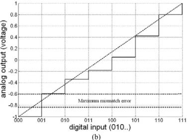
− = ⋅ ⋅ 2 dac σ (2.6)The characteristic of nonlinear DAC I/O transfer curve depends on two factors. The first is the DAC output error variance (2.6), as is demonstrated by Fig. 2.3 that larger output errors would result in an I/O curve which is more nonlinear. The second factor is the number of DAC output levels. Fig. 2.4 shows two I/O curves with the same output error variance, but Fig. 2.4 (b) is more nonlinear than Fig. 2.4 (a) because more levels in Fig. 2.4 (b) result in more variation.
(b)
Fig. 2.3 DAC transfer curve: (a) DAC with smaller DAC output error, and (b) DAC with larger DAC output error
(a)
(b) Fig. 2.4 DAC transfer curve: (a) DAC with fewer output levels, and (b) DAC with more output levels.
Accordingly, we propose to model DAC I/O relationship as
( ) ( ) cap sin( ( )
y nT =x nT
+
Δ⋅
a x nT⋅ +θ
) (2.7)where is related to variation magnitude demonstrated by Fig. 2.3, a is related to
variation frequency, and θ is a uniformly distributed random variable in representing possible horizontal shift. Then, utilizing Taylor’s series, (2.7) can be expanded as follows:
cap Δ [0,2π] 2 1 2 0 0 2 3 4 0 1 2 3 4 sin( ) ( ) ( ) cos ( 1) sin ( 1) (2 1)! (2 )! = ... cap n n n n cap cap n n a x ax ax n n a a x a x a x a x θ θ ∞ + θ ∞ = = Δ ⋅ ⋅ + = Δ × − + + Δ × − + + + + +
∑
∑
(2.8)Suppose x in (2.8) is a sinusoidal input. The harmonics distortion powers in y of (2.7) can be derived as follows: 2 2 4 6 6 2 4 15 1 2 s
2 2sin in 2sin in 32sin in DAC a a a HD A A A in2θ θ θ θ ⎛ ⎞ ⎜ ⎟ ⎜ ⎟ ⎝ ⎠ = + + +⋅⋅⋅ ⋅ 2 3 5 3 5 5 1 3 c 2 4cos in 16cos in DAC a a HD A A os2θ θ θ ⎛ ⎞ ⎜ ⎟ ⎜ ⎟ ⎝ ⎠ = + +⋅⋅⋅ ⋅ 2 4 6 6 4 3 1 4 s 2 8sin in 16sin in DAC a a HD A A in2θ θ θ ⎛ ⎞ ⎜ ⎟ ⎜ ⎟ ⎝ ⎠ = + +⋅⋅⋅ ⋅ (2.9)
Then, expressing the harmonics powers as their expected values, one obtains
2 2 4 4 6 6
[ 2DAC] 20log cap | 0.125 in 0.010415 in 0.0003255 in|
E HD ≅ Δ ⋅ − a A + a A − a A
3 3 5 5
[ 3DAC] 20log cap| 0.02083 in 0.00130208 in|
E HD ≅ Δ ⋅ − a A + a A
4 4 6 6
[ 4DAC] 20log cap |0.002604 in 0.00013021 in|
E HD ≅ Δ ⋅ a A − a A (2.10)
The expressions (2.10) suggest that, once , a, and Ain are fixed, DAC distortion powers
are determined, and can be expressed as PDAC_distotion = HD2DAC+HD3DAC+HD4DAC. For (2.10)
to be useful, we need to establish and a as functions of and u (=2B) is the number of unit DAC in Fig. 2.2. Behavior simulations are employed for this task, which is shown in
cap
Δ
cap
Fig. 2.5,
Fig. 2.5 Behavior simulation for DAC nonlinearity
where EDAC is obtained from Eq. (2.4) for each level and μ represents the finite DC-gain error.
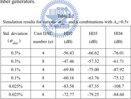
The simulation results of various and u combinations are shown in Table 2.2. Each
harmonic distortion power listed in Table 2.2 is the average of results from twenty simulation runs. These twenty simulations differ only in DAC mismatch errors ek which are generated
from random number generators.
dac
σ
Table 2.2
Simulation results for various σdac and u combinations with Ain=0.5v
Std. deviation (σdac) Unit DAC number (u) HD2 (dB) HD3 (dB) HD4 (dB) 0.3% 4 -56.43 -66.62 -76.01 0.3% 8 -47.46 -57.32 -61.71 0.1% 4 -69.88 -75.00 -87.92 0.1% 8 -60.16 -63.76 -75.12 0.025% 4 -83.58 -87.35 -108.7 0.025% 8 -72.77 -79.25 -84.60
By marking use of (2.10) and Table 2.2, after some efforts on comparison and calculation, we come up with the following equations:
0.707 cap u σdac Δ = ⋅ × 2 0.8 (0.59 in 0.263) (1.4667 0.125 0.0084 ) a= A − + ⋅ + ⋅ +u ⋅u (2.11)
model. In order to check our model to see if it is generally correct, we compare our model (2.10), (2.11) with behavior simulation results for other and u combinations to see if they closely match each other. Theoretical results from our model (2.10) and (2.11) and the corresponding simulation results are tabulated in Table 2.3.
dac
σ
Table 2.3
Theoretical results and simulation results for various σdac and u combinations with Ain=0.7v dac σ (%) u HD2 (dB) Simulation results HD2 (dB) Theoretical results HD3 (dB) Simulation results HD3 (dB) Theoretical results HD4 (dB) Simulation results HD4 (dB) Theoretical results 0.2 4 -61.34 -57.24 -67.85 -68.68 -82.16 -82.68 0.2 8 -54.23 -49.91 -55.87 -58.09 -63.85 -68.57 0.125 4 -60.89 -61.32 -71.71 -72.76 -84.42 -86.77 0.125 8 -57.83 -53.99 -62.98 -62.18 -70.96 -72.65 0.05 4 -73.85 -69.28 -80.96 -80.72 -88.30 -94.73 0.05 8 -64.91 -61.95 -74.15 -70.14 -76.45 -80.61
The theoretical and simulation results are mostly close and they confirm that our DAC distortion model is reasonable one.
Fig. 2.6 2-1 Mash architecture of SDM
MASH architecture shown in Fig. 2.6 cascades low order single loops modulator in order to get high order noise shaping effect. The output can be derived as follow:
3 3 1 2 1
1 1
( ) ( ) ( ) (1 ) ( )
Y z =z X z− +z N z− + −z− z N z− 2 (2.12)
where N1(z) and N2(z) are the noises and equivalent distortions generated by first and second
stage single loop SDM respectively. According to equation (2.12), the noises and equivalent distortions generated by second stage single loop SDM are subjected to noise shaping effect. Furthermore, the quantization noise of first stage single loop SDM is the input of second stage single loop SDM; hence SDM input signal will not affects the integrators of second stage single loop SDM. The harmonic distortion due to non-idealities in second stage single loop SDM can be significantly reduced [40]. For these reasons, the MASH output noise powers and nonlinear distortion powers are dominated by those of the first stage single loop modulator. Therefore, most MASH output non-ideality power models are the same as those discussed in Chapter 2, except finite DC-gain noise and capacitor mismatch noise. Models of finite DC-gain noise and capacitor mismatch noise need to be re-derived and they can be obtained from [28].
2.4 Non-idealities Models for Other Architecture
The Single-loop and MASH SDM discussed above are by far the most popular architectures. Non-ideality models for other special-purpose SDM architectures can also be systematically derived. In general, SDM non-idealities can be separated into two categories. Those in the first category are due to some noise sources; related power models can be derived by
2 - B ( ) | ( ) | B f noise f
Non ideality Power + S f H f df
−
=
∫
⋅ (2.13)where H(f) is the transfer function from noise source to SDM output, and Snoise(f) is the PSD
of noise source. Non-idealities in the second category involve some nonlinearity. Techniques used in [25], [26] and Appendix A can be reapplied to obtain power and distortion models.
3
Discussion of New Problems Associated to
Model-Based Designs
The SDM design spec. is typically given in terms of SNDR (3.1). SNDR is defined as
S N D P SNDR P P = + (3.1)
where PS represents the signal power, PN the total noise power and PD the total distortion
power. In simulation-based high level SDM designs, PN and PD are generated from behavior
simulations. In model-based approach, PN is computed by summing up each SDM output
noise power models described in Chapter 2, and PD is computed by summing up each SDM
output distortion power models described in Chapter 2. However, there are two issues associated with the computation of PN and PD:
1) Identifying essential models for model-based designs
Not every noise or distortion power model discussed in Chapter 2 should be included in PN or PD because some noise or distortion power models can be greatly suppressed by
various techniques. This issue will be discussed this chapter. 2) Quantizer overload problem
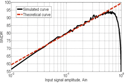
Ideally, SNDR is proportional to input signal amplitude Ain. In practice, quantizer
overload can significantly reduce SNDR after Ain grows certain point, as is shown in Fig.
Fig. 3.1 The performance of SNDR versus SDM input signal amplitude
3.1 Identifying Essential Non-idealities Models for Model-Based Designs
Among the models reviewed in Chapter 2, PCap_mismatch, POTA_flicker, PCap_distortion,
PSwitch_distortion, PRef_noise, PHysteresis and PSettling_distortion can be largely suppressed by various
techniques. PCap_mismatch can be greatly limited by the present CMOS technologies providing
the capacitor mismatch as good as 0.05%~1% [28]. POTA_flicker can be improved by decreasing
the corner frequency, and can be further reduced by the cancellation techniques such as correlated double sampling, chopper stabilization, and autozeroing [28]. Recently, PCap_distortion
can be improved by using stacked insulator structure of high-K and SiO2 dielectrics such as
HfO2/SiO2 stacked MIM capacitors [30]. PSwitch_distortion can be improved in many ways. One
way is to adjust switches size; another way is to improve linearity by using low VT devices or
clock boosting techniques [35], [36], [37]. PRef_noisecan be improved by connecting the large
bypass capacitor to the voltage reference buffer [31]. PHysteresis can be neglected in many
cases because it subjects to the same noise shaping effect as quantization noise in SDM [12]. Finally, we verified that PSettling_distortion is either negligible or orders smaller than PSettling_noise.
On the other hand, some of the models reviewed in Chapter 2 can be combined together. Due to finite-dc-gain may produce changes in noise transfer function and increase in-band quantization noise, PFinite_DC-gain and PQuantization_noise should be considered together and,
eventually, the modified quantization noise power for single-loop 2nd-order SDM could be formed as [13]: 2 4 2 _ _ 5 3 2 ( )( 12 5 3 LSB
Modified quantization noise
V P OSR OSR 2 ) π μ π = + (3.2)
where μ represents the finite DC-gain error, and 2
2 ref
LSB B
V
V = represents the quantizer step
size for mid-tread quantizer.
From the discussion above, the PN and PD in (3.1) can be determined as
_ _ _
_ _
_ _
N Modified quantization noise Switch thermal
Jitter noise DAC noise
OTA thermal Settling noise
P
P
P
P
P
P
P
=
+
+
+
+
+
(3.3) and - _ _D DC gain distortion DAC distortion
P
=
P
+
P
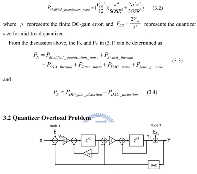
(3.4)3.2 Quantizer Overload Problem
Fig. 3.2 The block diagram of 2nd-order single-loop SDM
If quantizer input amplitude exceeds Vref, the PQuantization_noise and PQuantization_distortion will
increase significantly, resulting in overload problem shown in Fig. 3.1. Overload problem can be easily avoided in behavior simulation because the magnitude of quantizer input can be easily observed. For model-based SDM designs, however, a method is needed to estimate the maximum SDM input amplitude allowed, in order to avoid quantizer overload problem.
To check the occurrence of overload, we need to observe signal Y1 in Fig 3.2, which can be
expressed as
2 2 1 2
1( ) ( ) ( 2 ) Q( ) ( )
In (3.5), Y1(z) consists of three parts. First part is the SDM input X(z) followed by unity gain
transfer function; hence X(z) directly affects Y1 swing. Second part is white noise E(z)
followed by unity gain transfer function. This part can be neglected due to the magnitude of E is typically very small for median to high resolution SDM. For example, a 15 effective number of bit design results in white noise smaller than -80dB which equals to the variance of
E; hence the standard deviation of E is
8
( )E 10 10
σ = − = −4
(3.6)
Since E is typically of Gaussian distribution, the three sigma magnitude contains 99.73% of random number. The magnitude of E can be set as
8
3 ( ) 3 10σ E = − =0.0003
(3.7)
which is very small compared with X. Third part is the sum of two independent time sequences eq(n-2) and 2eq(n-1), denoted by q1(x) and q2(y). The probability density functions
(pdf) of q1 and q2 are shown in Fig. 3.3. Suppose q(n)=q1(x)+q2(y), the distribution function
of q(n) is 1 2 1 2 ( ) ( ) ( , ) n y q q F n P q q n f x y dxdy − ∞ −∞ −∞ = + ≤ =
∫ ∫
q (3.8)Taking the derivation with to the random variable n, we obtained 1 2 [ ( )] ( ) q ( , ) q q q d F n f n f n dn ∞ −∞ = =
∫
−y y dy (3.9)Due to the random variable q1(x) and q2(y) are statistically independent, Eq. (3.9) is modified
to be 1 2 1 2 ( ) ( , ) ( ) ( ) q q q q q f n f n y y dy f n y f y dy ∞ ∞ −∞ −∞ =
∫
− =∫
− (3.10)Eq. (3.10) indicates that the swing of node Y1 can be obtained by convoluting f xq1( ) and
2( ) q
f y , which is shown in Fig. 3.4 (a). Thus, the swing of node Y1 due to quantization
been verified by behavior simulation. For Vref =1 and B=2, the corresponding simulation result is shown in Fig. 3.4 (b). (b Fig. 3.3 (a) (a) ) 1( ) q f x The pdf of q1(n) (b) fq2( )y The pdf of q2(n). (a) (b)
Fig. 3.4 (a) The theoretical pdf of q(n) (b) The simulated distribution of q(n).
From discussions above, the signal swing at quantizer input can be estimated to be 3 2 LSB SW in V V = +A (3.8)
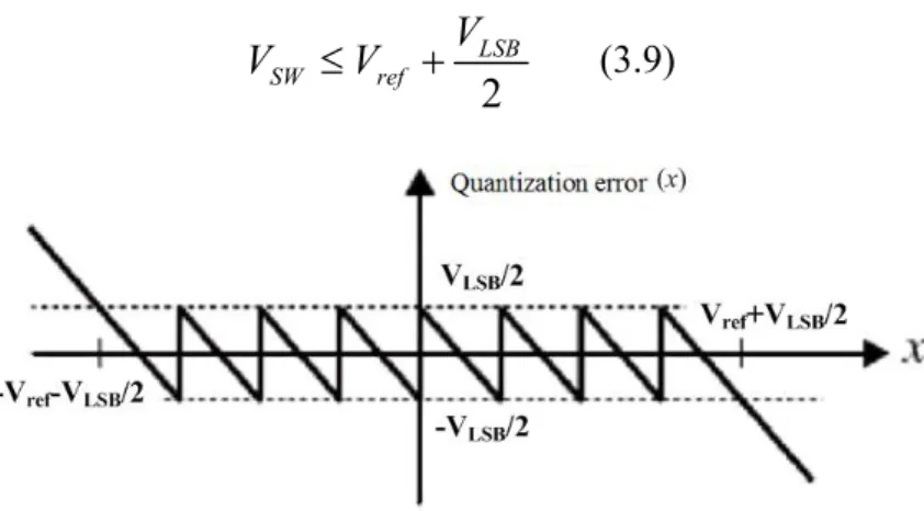
In order to avoid quantizer overload, VSW needs to satisfy 2 LSB SW ref V V ≤V + (3.9)
Fig. 3.5 Quantizer error function v.s quantizer input signal
Eq. (5) comes from the fact shown in Fig. 3.5 that quantizer error grows unbounded when VSW
exceeds the RHS of (3.9). When B≧2, Eq. (3.9) determines the largest allowed Ain to be
in ref LSB
A ≤V −V (3.10)
Eq. (3.9) is verified by behavior simulation w. r. t. different bit number with Vref=1. The result
is listed in Table 3.1.
TABLE 3.1
Simulation results and theoretical results for various B
Bit number Simulation result of maximum allowed Ain Theoretical result of maximum allowed Ain 2 0.56 0.5 3 0.81 0.75 4 0.9 0.875
The case for B=1 needs special attention, since quantizer overloads for all Ain except Ain=0.
But it is indicated in [12] that the excess noise due to overloading the quantizer increases quite slowly; hence there is a margin linearly related to Vref for one bit quantizer. We evaluated
this margin to be 0.36 Vref by behavior simulation. Therefore, for one bit case, Eq. (3.10) is
modified to be
1.36
in ref LSB
4
An Example for High-Level Synthesis of DT
SDM Based On Model-Based Designs
In this Chapter, we propose a methodology for model-based SDM design optimization. This design method is applied to a published design task [34]. Compared with the MASH SDM reported in [34], the SDMs designed by our method achieves much higher SNDR and significantly lower power consumption. This shows that our method can effectively achieve more balanced designs for piratical applications.
4.1 Design Optimization Schemes
A typical SDM design optimization algorithm is reference to [41]
4.2 Example for ΣΔ ADC for 14-bit 2.2-MS/s
The MASH SDM design specs reported in [34] to be achieved are
z Peak SNDR : 72 dB
z Signal bandwidth : 1.1 MHz
According to [34], Vref and VDD are set at 1V and 3.3V for the 0.35-μm CMOS technology.
Design parameter space searched by our model-based optimization scheme is
z B: 1 ~ 4 z OSR: 4~24 z CS: 0.1 ~1.32 pF
z A0: 45 ~ 53 dB
z SR: 50 ~ 475 V/μs z Ain: 0.1 ~ 1 V
The results published in [34] and that achieved from our methodology are all listed in Table VII.
TABLE 4.1
COMPARISONS OF OUR DESIGN RESULTS WITH THOSE IN [34]
Design parameters Reference [34] K = 1 Unit
B (second stage) 5 1 - B (first stage) 1 2 OSR 24 24 - CS 1.32 1.19 pF A0 53 53 dB GBW 1000 120 MHz SR 475 150.8 V/μs Ain 0.55 0.47 V SNDR reported in [34] 72 - dB SNDR(Our model) 75.64 82.897 dB SNDR(Simulink) 76.585 82.66 dB POWER(Our model) 207.14 24.0304 mW
1. The optimization result compared to [34] demonstrates that our methodology helps designers to design MASH SDM. The concepts for designing MASH SDM focus on the optimization design of first stage single loop SDM and relax the design parameters on second stage single loop SDM, and the analysis of the optimization result compared to [34] is almost the same as the previous one. In addition, the modified quantization noise needs to be carefully taken into account due to the quantization noise rely heavily on the leakage of MASH SDM.
5
Conclusions
The main contributions in this paper are described in the following. First, an overview of the non-idealities power models of 2nd order single loop SDM and MASH SDM was presented, which shows that mathematical models were quit complete for model-based designs. Then, the quantizer overload model could provide that the obtained results of Ain and
SNR from model-based designs could be more similarly to realistic DT SDM, and could
indicate the distribution of different nodes of SDM, which maybe helpful in statistical properties. Furthermore, model-based designs can potentially be at the order of 104 times faster, which can search much more design parameters combination than simulation-based designs over the same period. Model-based designs also can explicitly compute each noise and distortion power, which could demonstrate the dominate non-idealities for designers to reduce the non-idealities by adjusting design parameters or using some circuit techniques. The non-idealities power models are currently being developed for other SDM architectures.
Appendix
A.1 an Approach for Extracting Sine Wave Signal from Any Order SDM
Output (Behavior Simulation)
The sine wave signal from the SDM output can be extracted by the following equations.
0 0 0 0 0 0
[ 2* ( )*(sin( ( )) ( ))*cos( ) ]*cos( )
( )
[ 2* ( )*(sin( ( )) ( ))*sin( ) ]*sin( )
( )
{ 2* ( )*[sin( )*cos( ) cos( )*sin( ) ( )]*cos( ) }*cos( )
( ) T T T T T T T w t t c N t t dt t T w t dt T w t t c N t t dt t T w t dt T w t t c t c N t t dt t T w t dt ω ω ω ω ω ω ω ω ω ω ω ω − + + − + = − + +
∫
∫
∫
∫
∫
∫
0 0 2 0 0 0{ 2* ( )*[sin( )*cos( ) cos( )*sin( ) ( )]*sin( ) }*sin( )
( )
[2* ( )*sin( )*cos( )*cos( ) 2* ( )*cos ( )*sin( )
{ } 2* ( )* ( )*cos( )] ( ) [2* ( { ( ) T T T T T T w t t c t c N t t dt t T w t dt w t t t c w t t c T dt t w t N t t T w t dt w T T w t dt ω ω ω ω ω ω ω ω ω ω ω *cos( )ω ω − + − = + +
∫
∫
∫
∫
∫
2 0)*sin ( )*cos( ) 2* ( )*cos( )*sin( )sin( )
}*sin( ) 2* ( )* ( )*sin( )]
{0 2*0.5*sin( ) 0}*cos( ) {2*0.5*cos( ) 0 0}*sin( ) -sin( )*cos( ) cos( )*sin( ) sin( ( ))
T t t c w t t t c dt t w t N t t c t c t c t c t t c ω ω ω ω ω ω ω ω ω ω ω ω ω ω ω ω − + = − + + − + = + = −
∫
The SDM output expresses as Sin(ω(t-c))+N(t), N(t) is the noise in SDM, w(t) indicates
window function and c is constant delay depending on the SDM order. The MATLAB code is written as
signal=(N/sum(w))*sinusx(vout(1:N).*w,fnormal,N); % Function of sinusx is used to extract sinusoidal
function outx = sinusx(in,fnormal,n)
% in: Input data vector
sinx=sin(2*pi*fnormal*[1:n]); % sin(W*N*T) cosx=cos(2*pi*fnormal*[1:n]); % cos(W*N*T) in=in(1:n); a1=2*sinx.*in'; a=sum(a1)/n; b1=2*cosx.*in'; b=sum(b1)/n; outx=a.*sinx + b.*cosx;
A.2 Error Function
Settling noise power model [26] contains many integral equations which can be expended to increase the speed for model-based design. The hardest integral equation for expending is
Fortunately, such error function can be expended by Taylor series as
References
[1] R. Schreier and G. C. Temes, Understanding Delta-Sigma Data Converters, New York: WILEY-IEEE Press, 2005
[2] J. Ruiz-Amaya, J. M. de la Rosa, F. V. Fernandez, F. Medeiro, R. del Rio, B. Perez-Verdu, and A. Rodriguez-Vazquez, "High-level synthesis of switched-capacitor, switched-current and continuous-time Sigma Delta modulators using SIMULINK-based time-domain behavioral models," IEEE Trans. Circuits
and Syst. I, Reg. Papers, vol. 52, pp. 1795-1810, Sep 2005.
[3] H. Zare-Hoseini, et al., "Modeling of switched-capacitor delta-sigma Modulators in SIMULINK," IEEE
Trans. Instrum. Meas., vol. 54, pp. 1646-1654, Aug. 2005.
[4] Y. Geerts and W. M. C. Sansen, Design of Multi-Bit Delta–Sigma A/D Converters. Norwell, MA: Kluwer, 2002.
[5] G. R. Boyle, D. O. Pederson, B. M. Cohn, and J. E. Solomon, "Macromodeling of integrated circuit operational amplifiers," IEEE J. Solid-state Circuits, vol. SC-9, pp. 353-364, 1974.
[6] J. C. Lin and J. H. Nevin, "A modified time-domain model for nonlinear analysis of an operational amplifier," IEEE J. Solid-State Circuits, vol. 21, pp. 478-483, 1986.
[7] L. A. Williams, III and B. A. Wooley, "MIDAS-a functional simulator for mixed digital and analog sampled data systems," in IEEE Symp on Circuit and Syst., May. 1992, pp. 2148-2151.
[8] G. T. Brauns, R. J. Bishop, M. B. Steer, J. J. Paulos, and S. H. Ardalan, "Table-based modeling of delta-sigma modulators using ZSIM," IEEE Trans. Comput.-Aided Des. Integr. Circuits Syst., vol. 9, pp. 142-150, Feb. 1990.
[9] C. M. Wolff and L. R. Carley, “Simulation of delta-sigma modulators using behavioral models,” in Proc.
IEEE Int. Symp. on Circuits Syst., May 1990, pp. 376-379.
[10] V. Libera li, V. F. Dias, M. Ciapponi, and F. Maloberti, "TOSCA: a simulator for switched-capacitor noise-shaping A/D converters," IEEE Trans. Comput.-Aided Des. of Integr. Circuits and Syst., vol. 12, pp. 1376-1386, 1993.
[11] P. Malcovati, S. Brigati, F. Francesconi, F. Maloberti, P. Cusinato, and A.Baschirotto, “Behavioral modeling of switched-capacitor sigma–delta modulators,” IEEE Trans. Circuits Syst. I, Fundam. Theory
Appl., vol. 50, no. 3, pp. 352–364, Mar 2003.
[12] S. R. Norsworthy, R. Schreier, G. C. Temes, Delta-Sigma Data Converters. Theory, Design and Simulation, New York: Wiley-IEEE Press, 1997.
[13] F. Medeiro, B. P. Verdu, and A. R. Vasquez, Top-Down Design of High-Performance Sigma-Delta
Modulators. Boston, MA: Kluwer, 1999.
[14] K. Francken and G. G. E. Gielen, "A high-level simulation and synthesis environment for ΔΣ modulators,"
IEEE Trans. Comput.-Aided Des. Integr. Circuits and Syst., vol. 22, pp. 1049-1061, 2003.
[15] F. Medeiro, B. Perez-Verdu, A. Rodriguez-Vazquez, and J. L. Huertas, "A vertically integrated tool for automated design of ΣΔ modulators," IEEE J. Solid-State Circuits, vol. 30, pp. 762-772, July. 1995.
[16] L. Jian-ming, D. Xiao-wu, Z. Xue-cheng, and Z. Zhi-ge, "Modeling Non-idealities of Sigma Delta ADC in simulink," in Proc. Int. Conference on Circuits and syst., ICCCAS, May 25-27, 2008, pp. 1040 - 1043. [17] S. Brigati, F. Francesconi, P. Malcovati, D. Tonietto, A. Baschirotto,and F. Maloberti, “Modeling
sigma-delta modulator non-idealities in simulink,” in Proc. Int. Symp. Circuits and Syst., ISCAS’99, 1999, vol. 2, pp.384–387.
[18] Zare-Hoseini, H., Shoai, O., Kale, I., “Precise Behavioral Modeling of High-Resolution Switched-Capacitor Σ-Δ Modulators,” in Proc. Instrum. and Meas. Technology Conference, IMTC Como, Italy, 18-20 May 2004.
[19] R. Castro-Lopez, F. V. Fernandez, F. Medeiro, and A. Rodriguez-Vazquez, "Accurate VHDL-based simulation of ΣΔ modulators," in Proc. Int. Symp. on Circuits and Syst., ISCAS '03, May 2003, vol. 4, pp. IV-632-IV-635
[20] G. Monnerie, H. Levi, N. Lewis, and P. Fouillat, "Behavioral modeling of noise in discrete time systems with VHDL-AMS application to a sigma-delta modulator," IEEE Int. Conference Industrial Technology,
ICIT '04, Dec 2004,vol. 1, pp. 237-242
[21] G. Suarez and M. Jimenez, "Behavioral modeling of ΣΔ modulators using VHDL-AMS," in Midwest Symp.
Circuits and Syst., MWSCAS, Aug 2005, vol. 1, pp. 704-707
[22] H. Y. Chu, C. H. Yang, C. W. Leng, and C. H. Tsai, "A top-down, mixed-level design methodology for CT BP ΣΔ modulator using verilog-A," IEEE Asia Pacific Conference on Circuits and Syst., APCCAS 2008., 2008, pp. 1390-1393.
[23] G. Suárez, M. Jiménez, and F.O. Fernández, “Behavioral modeling methods for switched-capacitor ΣΔ modulators,”IEEE Trans. Circuits Syst. I, Reg. Papers, vol. 54, no. 6, pp. 1236–1244, Jun 2007
[24] R. Storn and K. Price, “Differential Evolution—A Simple and Efficient Adaptive Scheme for Global Optimization over Continuous Spaces,” Technical Report TR-95-012, International Computer Science Institute, Berkely, 1995.
[25] F. C. Chen and C. L. Hsieh, "Modeling Harmonic Distortions Caused by Nonlinear Op-Amp DC Gain for Switched-Capacitor Sigma-Delta Modulators," IEEE Trans. Circuits and Syst. II: Exp. Briefs, vol. 56, pp. 694-698, 2009.
[26] F. C. Chen and C. C. Huang, "Analytical Settling Noise Models of Single-Loop Sigma-Delta ADCs," IEEE
Trans. Circuits and Syst. II: Exp. Briefs, vol. 56, pp. 753-757, 2009.
[27] Y. Wei,Subhajit Sen, and Bosco H.Leung,. "Distortion analysis of MOS track-and-hold sampling mixers using time-varying Volterra series,"IEEE Trans. Circuits and Syst. II: Analog and Digital Signal Processing, vol. 46, pp. 101-113, 1999.
[28] R. del Río, F. Medeiro, B. Pérez-Verdú, J. de la Rosa, and R.-V. Á., CMOS Cascade Sigma-Delta
Modulators for Sensors and Telecom: Error Analysis and Practical Design. Dordrecht, Netherlands:
Springer, 2006.
[29] B. E. Boser and B. A. Wooley, "The design of sigma-delta modulation analog-to-digital converters," IEEE J.
[30] S. J. Kim, B. J. Cho, M. F. Li, S.-J. Ding, M. B. Yu, C. Zhu, A. Chin, and D.-L. Kwong, “Engineering of voltage nonlinearity in high-k MIM capacitors for analog/mixed-signal ICs,” in VLSI Symp. Tech. Dig., 2004, pp. 218–219.
[31] B. Razavi, Design of Analog CMOS Integrated Circuits. New York: McGraw-Hill, 2000.
[32] Jorge I. Aunon and V. Chandrasekar. Introduction to Probability and Random Processes, 1st ed., New York: McGraw-Hill, 1996.
[33] R. Gaggl, et al., "A 85-dB dynamic range multibit delta-sigma ADC for ADSL-CO applications in 0.18-μm CMOS," IEEE J. Solid-State Circuits, vol. 38, pp. 1105-1114, 2003.
[34] J. Morizio,M. Hoke,T. Kocak,C. Gedd ie,J. Perry,S .Madhavapeddi,M.H. Hood,G. Lynch, H. Kondoh, T. Okuda, H. Noda, M. Ishiwaki, T. Miki, and M. Nakaya,"14-bit, 2.2MS/s sigma delta ADCs," IEEE
J.Solid-State Circuits, vol. 35, pp. 968-976, July 2000
[35] C.C. Hung and C.Y. Yang, “A Low-Voltage Low-Distortion MOS Sampling Switch,” in Proc. IEEE Int.
Symp. on Circuits and Syst., ISCAS 2005, 2005, vol. 4, pp. 3131-3134.
[36] J. Steensgaard, ”Bootstrapped low-voltage analog switches,” in Proc. IEEE Int. Symp on. Circuits and
Syst., ISCAS’99, 1999, vol. 2, pp. 29- 32.
[37] K. Ong, V. I. Prodanov, and M. Tarsia, “A method for reducing the variation in “on” resistance of a MOS sampling switch,” in Proc. Int. Symp.Circuits and Syst., ISCAS2000, 2000, vol. 5, pp. 437 – 440.
[38] Paul R. Gray, Paul J. Hurst, Stephen H. Lewis and Robert G. Meyer, Analysis and design of analog
integrated circuits, 4th ed., John Wiley & Sons, Inc., 2001
[39] Y. Geerts, M. Steyaert, and W. Sansen., "A 12-bit 12.5 MS/s multi-bit ΔΣ CMOS ADC," in Proc. IEEE 2000 Custom Integr. Circuits Conference, CICC., 2000, pp. 21-24.
[40] L. Yao, M. Steyaert, and W. Sansen, Low-Power Low-Voltage Sigma-Delta Modulators in Nanometer
CMOS. New York: Springer, 2006.
[41] 國立交通大學電機與控制工程研究所, Tzu-En Sheng, “Noise Correlation Model and Model-based Design