國 立 交 通 大 學
機 械 工 程 學 系
博士論文
電鍍鎳-鑽奈米複合材料之
熱膨脹係數及疲勞特性研究
Investigation on Coefficient of Thermal Expansion and Fatigue
Properties of Electroplated Ni-diamond Nanocomposite
研 究 生:黃家聖
指導教授:徐文祥、鄭裕庭
電鍍鎳-鑽奈米複合材料之熱膨脹係數及疲勞特性研究
Investigation on Coefficient of Thermal Expansion and Fatigue Properties of
Electroplated Ni-diamond Nanocomposite
研 究 生:黃家聖 Student: Chia-Sheng Huang
指導教授:徐文祥 Advisors: Wensyang Hsu
鄭裕庭
Yu-Ting Cheng
國 立 交 通 大 學
機 械 工 程 學 系
博 士 論 文
A Dissertation
Submitted to Department of Mechanical Engineering College of Engineering
National Chiao Tung University in partial Fulfillment of the Requirements
for the Degree of PhD in Mechanical Engineering October 2009 Hsinchu, Taiwan
中華民國 九十八 年 十 月
電鍍鎳-鑽奈米複合材料之熱膨脹係數及疲勞特性研究
學生:黃家聖 指導教授:徐文祥
鄭裕庭
國立交通大學機械工程學系 博士班
摘 要
電鍍鎳是微機電系統裝置中,常見的結構材料。近來更因為奈米科技的發展,結 合奈米顆粒形成複合材料,不但強化了原先材料的特性,也增廣了電鍍鎳的應用範 圍。在本論文中,將針對電鍍鎳-鑽奈米複合材料,於其熱膨脹係數變化機制、材料 應用、材料可靠度議題等方面,做一完整的探討與研究。 於熱膨脹係數變化機制方面:利用文獻和 X 光繞射實驗的相互比對下,電鍍鎳 基奈米複合材料內的殘留應力類型,可以藉由 X 光繞射角之峰值變化定義之,且被 認定為最有可能影響奈米複合材料之熱膨脹係數變化的因素。而且此一來自製程的殘 留應力,其類型可以由鎳基材與添加顆粒間的硬度差異或楊氏係數差異驗證之。根據 實驗量測結果,電鍍鎳基材結合奈米鑽石顆粒,所形成的奈米複合材料呈現殘留壓應 力,其熱膨脹係數可由原先電鍍鎳的23 ×10-6/°C 提升至 50.1 ×10⁻⁶/°C;相對地,當電 鍍鎳基材結合奈米二氧化矽顆粒,所形成的奈米複合材料則呈現殘留張應力,其熱膨 脹係數由原先電鍍鎳的23 ×10-6/°C 減少至 18 ×10-6/°C。 於材料應用方面:利用雙層板效應,電鍍鎳-鑽奈米複合材料的熱膨脹係數特性 已被應用於一新型的鎳基熱雙層結構上。當熱雙層結構由電鍍鎳和電鍍鎳-鑽奈米複 合材料疊合而成時,藉由電鍍鎳和電鍍鎳-鑽奈米複合材料兩者電鍍順序的調換,即 可簡單地製作出向上或向下致動的熱雙層結構。加上這兩層鎳基材料具有相似的晶格 結構的和相同的電鍍沈積溫度,其所製成的熱雙層結構,由實驗測試結果可知,擁有 較佳的界面結合力和較低的熱殘留熱應力。 於材料可靠度議題方面:利用微機電製程與電鍍技術,分別製作電鍍鎳和電鍍鎳 -鑽奈米複合材料的微懸臂樑測試試片,藉由出平面彎曲測試的方法,討論電鍍鎳與 電鍍鎳-鑽奈米複合材料的疲勞特性與楊氏係數特性。根據實驗量測結果得知,由於 奈米顆粒的添加,使得材料的延性降低,造成複合材料的疲勞強度略低於鎳基材;然 而,當所添加的奈米顆粒尺寸由350 nm 降至 50 nm 時,顆粒的尺寸效應則可使電鍍 鎳-鑽奈米複合材料有~13.6%的楊氏係數提升,且具有與電鍍鎳可相比較的疲勞強度 (~2.4 GPa)。Investigation on Coefficient of Thermal Expansion and Fatigue Properties of
Electroplated Ni-diamond Nanocomposite
Student: Chia-Sheng Huang Advisors: Wensyang Hsu
Yu-Ting Cheng
Department of Mechanical Engineering
National Chiao Tung University
Abstract
Electroplated Ni is the common structure material in MEMS devices. Recently, the nanotechnology has advanced it for enhanced material properties and wide applications by incorporated nano-particles. In this dissertation, the electroplated Ni-diamond nanocomposite has been investigated thoroughly in terms of CTE variation mechanism, material application, and reliability issue.
For the CTE variation mechanism, through the XRD investigation, residual stress types of Ni-based nanocomposites can be determined. These residual stresses resulted from co-deposited process are thought as the promising factor to affect the CTE variations. According to measurement results, the incorporated nano-diamond particles in Ni matrix will enhance the CTE of electroplated Ni from 23 to 50.1 ×10⁻⁶/°C with residual compressive stress; oppositely, the incorporated nano-SiO2 particles in Ni matrix will diminish the CTE of electroplated Ni from 23 to 18 ×10-6/°C with residual tensile stress.
For the material application, the CTE property of Ni-diamond nanocomposite is applied on a newly Ni-based thermal bimaterial structure by bimorph effect. Thermal bimaterial structure made of electroplated Ni/Ni-diamond nanocomposite can achieve upward and downward out-of-plane displacement easily by controlling the plating sequence of electroplated Ni and Ni-diamond nanocomposite. Since Ni and Ni-diamond nanocomposite have different CTE but similar crystal structure and process temperature, the fabricated thermal bimaterial structures show better interfacial bonding strength and smaller residual thermal stress.
For the reliability issue, the characterizations of fatigue and Young’s modulus have been studied employing the bending-test method on the specimens made of electroplated Ni and Ni-diamond nanocomposites. According to the measurement results, Ni-diamond nanocomposite has slightly smaller fatigue strength than that of pure electroplated Ni due to the ductility reduction resulted by the nanoparticles. However, once the particle size of nano-diamond is reduced from 350 to 50 nm, it has been found that the electroplated Ni-diamond nanocomposite can have higher Young’s modulus (~13.6% enhancement) and comparable fatigue strength (~2.4 GPa) with that of pure electroplated Ni.
誌 謝
讀博士班就像跑馬拉松一樣,在孤寂的喘息聲中,一步步地考驗著自我的耐力與 毅力。在這漫長的路程,最值得感謝的是沿途的啦啦隊、補給站以及加油的人群,讓 我隨時能補充體力與活力跑完全程。所以這份榮耀,並不單單屬於我自已。在此,我 希望藉由以下文字分享此份榮耀,衷心地紀錄和感謝一路上曾幫助我、關心我的朋友 與家人。 首先,我要感謝我的指導教授:徐文祥老師。沒有他的知遇之恩,就沒今日的我。 從碩士班到博士班這七年多的時間,老師除了提供無虞匱乏的實驗資源外,更盡心竭 力地在研究上給予指導。而老師對於事物的剖析與獨特的見解,總令我印象深刻,我 多麼希望時間可以暫停,好讓我能從他身上多挖一些寶石,以做為未來人生歷鍊的基 石。 同時,我要感謝我的另一位指導教授:鄭裕庭老師。積極、有衝勁的他,在研究 方法與論文撰寫方面的專業與態度,令我沒齒難忘也獲益良多。對我來說,老師就像 生命中的貴人一樣,每當我的研究山重水複疑無路之時,他總是能適時、關鍵地指引 我柳暗花明又一村。 其次,我要感謝清大材料黃振昌老師、師大機電楊啟榮老師、逢甲機電劉顯光老 師,以及交大機械徐瑞坤老師、周長彬老師,在百忙之中願意擔任我博士論文的口試 委員,並提供我許多研究上的寶貴意見。藉由口試的問答,老師們給了我許多不同觀 點的想法,也讓我思考到許多沒注意到的問題。雖然口試時間短暫,但卻讓我獲益匪 淺。 再次感謝徐文祥老師,因為有他,所以在這時空,我才能有這福氣和許多的實驗 室夥伴相遇、共事。也因為有這些實驗室夥伴當後盾,我才能堅穩地跨出每一步。在 這些實驗室夥伴中,感謝鍾君煒學長、楊涵評學長、邱雅惠學姐、蔡梨暖學姐、林郁 欣學長、張駿偉學長、李毅家學弟、黃元德學弟、葉昌旗學弟,在專業知識上的解惑,與實驗研究上的幫助。感謝葉昶志學弟與逢甲機電林瑜婷學妹的情義相挺,颱風夜仍 堅守崗位,無怨無悔地幫我完成疲勞實驗,真的很感恩。感謝林軒宇學弟、胡皓宇學 弟、蔣鎧宇學弟、廖淳旭學弟、王澤瑋學弟、吳松岳學弟、黃正鄴學弟,有了這些嗨 咖學弟,實驗室總是充滿歡樂與活力,和他們相處的日子是我最快樂的時光。感謝鄭 裕庭老師實驗室的陳永昌學弟與范士岡老師實驗室的許耀文學弟,和我一起作伴去美 國參加會議、瘋狂購物,也一起吃到難吃的牛排。 這研究能完成,還要感謝交大奈米中心、國家奈米元件實驗室、國家晶片系統設 計中心、國家儀器科技研究中心、勤益科大潘吉祥老師、逢甲機電劉顯光老師,提供 代工服務、製程與量測設備。 最後,我要衷心地感謝養育我的銀河爸爸和月卿媽媽,謝謝家芯妹妹和家鴻弟 弟,謝謝月華阿姨、月霞阿姨、劉傳姨丈,感謝你們的支持與關心、加油與鼓勵。還 有最重要的是,感謝瓊慧能耐心地陪我走過這段艱辛的日子,謝謝妳為我所承受及付 出的一切。 ~ 謹以本論文,獻給一路上曾幫助我和關心我的朋友與家人。謝謝你們,感恩。 ~ 家聖 于 新竹.交大 2009/10/10
Content
摘 要 ... i
Abstract ...ii
誌 謝 ...iii
Content ... v
List of Tables ...vii
List of Figures ...viii
Chapter 1 Introduction ... 1
1.1 Motivation ... 1
1.2 Background... 3
1.2.1 Electroplated Ni-diamond Nanocomposite ... 3
1.2.2 Fatigue Test Methods... 6
1.3 Dissertation Outline... 9
Chapter 2 Investigation on CTE Property ... 14
2.1 Introduction ... 14
2.1.1 Rule of Mixtures... 14
2.1.2 Particle Effect ... 17
2.1.3 Factors that Affect CTE... 17
2.2 Measurements and Discussions... 19
2.2.1 Grain Size Measurement ... 19
2.2.2 Stress Mode Investigation ... 20
2.3 Summary... 22
Chapter 3 Application of CTE Property on Bimorph Effect... 30
3.2 Bimaterial Structure Design ... 31
3.3 Bimaterial Structure Fabrication ... 33
3.4 Measurements and Discussions... 35
3.4.1 Thermal Performance Measurement ... 35
3.4.2 Interlaminar Reliability Test... 37
3.4.3 Electro-thermal Driven Discussion ... 38
3.5 Summary... 39
Chapter 4 Investigation on Fatigue Property ... 51
4.1 Introduction ... 51
4.2 Experiment Setup ... 52
4.3 Specimen Preparation... 53
4.4 Measurements and Results ... 54
4.4.1 Static Bending Test ... 54
4.4.2 Young’s Modulus Measurement ... 55
4.4.3 Fatigue Test... 56
4.5 Discussions ... 57
4.6 Summery... 60
Chapter 5 Conclusion... 71
5.1 Summary... 71
5.2 Future Research Direction... 73
Reference ... 74
List of Tables
Table 2.1 Plating bath conditions of Ni-based nanocomposites... 24 Table 2.2 Parameters derived from XRD investigation on Ni-based nanocomposite. ... 24 Table 3.1 Plating bath conditions of Ni and Ni-diamond nanocomposite for structural
layers of thermal bimaterial structure... 41 Table 3.2 CTE and Young’s modulus of each structural layer of thermal bimaterial
structures... 41 Table 4.1 Plating bath conditions of Ni-based materials for microsized cantilever-beam
specimens. ... 62 Table 4.2 Young’s moduli of electroplated Ni and Ni-diamond nanocomposites derived
from F−δ curves, nanoindenter measurement, and resonant frequency
List of Figures
Figure 1.1 Mechanism of particles co-deposition into a metal deposit. [7] ... 10
Figure 1.2 Fatigue test apparatus for making rotating-bending test. [21] ... 10
Figure 1.3 Common fatigue test types classified by loading methods. ... 11
Figure 1.4 In-plan tensile method of fatigue test: test machine and specimen. [22] ... 11
Figure 1.5 In-plan tensile method of fatigue test: (a) test system, and (b) schematic diagram of specimen. [23]... 11
Figure 1.6 In-plan tensile method of fatigue test: (a) test system, and (b) schematic dog-bone shape sample. [24] ... 12
Figure 1.7 In-plan bending method of fatigue test: fatigue test device integrated with test beam and electrostatic actuator. [15] ... 12
Figure 1.8 Out-of-plan bending method of fatigue test: block diagram of test system and microsized specimens without/with notch. [25] ... 13
Figure 2.1 Comparison between experimentally measured data and theoretically predicted calculations of CTE values of Ni-diamond nanocomposites... 25
Figure 2.2 Comparison of CTE properties between pure electroplated Ni and Ni-SiO2 nanocomposites with different particle concentration. [13] ... 25
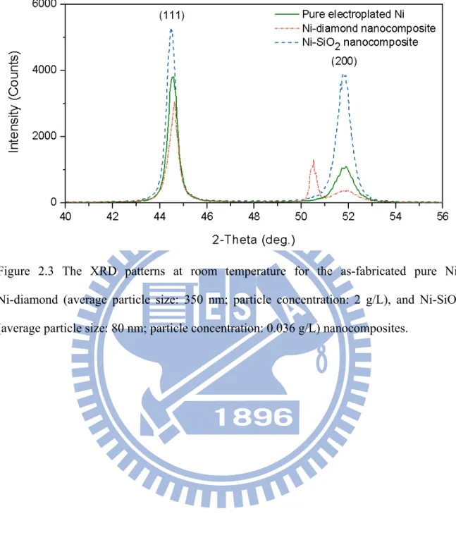
Figure 2.3 The XRD patterns at room temperature for the as-fabricated pure Ni, Ni-diamond (average particle size: 350 nm; particle concentration: 2 g/L), and Ni-SiO2 (average particle size: 80 nm; particle concentration: 0.036 g/L) nanocomposites. ... 26
Figure 2.4 Principle of (a) microstrain measurement by XRD peak broadening; (b) macrostrain measurement by XRD peak shift... 27
Figure 2.5 Comparison of hardness between electroplated Ni and Ni-based
nanocomposites including Ni-diamond and Ni-SiO2 with different particle
sizes and concentrations. [12, 13]... 28 Figure 2.6 Comparison of Young’s moduli between electroplated Ni and Ni-based
nanocomposites including Ni-diamond and Ni-SiO2 with different particle
sizes and concentrations. [12, 13]... 28 Figure 2.7 Resulted residual stress type from particle and matrix in Ni-based
nanocomposite: (a) compressive stress in Ni-diamond; (b) tensile stress in
Ni-SiO2. ... 29 Figure 3.1 Schematic illustration of Ni-based thermal bimaterial structures including
upward and downward deflection types. ... 42 Figure 3.2 Calculated themomechanical sensitivity of thermal bimaterial structure for
layer thickness determination. ... 42 Figure 3.3 Fabrication process of thermal bimaterial structure: (a) 5 μm AZP-4620 PR
deposition and patterning; (b) sputtered Ti/Cu as an adhesion and seed layer, then 15 μm AZP-4620 PR deposition and patterning as the plating mold structure; (c) layers electroplating: Ni-diamond nanocomposite for bottom layer, and Ni for top layer (i.e. upward type); (d) structure releasing; (e) silicon removing by KOH. ... 43 Figure 3.4 SEM pictures of fabricated thermal bimaterial structures: (a) upward type: Ni
layer on top of Ni-diamond nanocomposite layer; (b) downward type:
Ni-diamond nanocomposite layer on top of Ni layer. ... 44 Figure 3.5 Schematic diagram and photo of set-up for thermal performance
Figure 3.6 Thermal performance measurement results and fitting curves in terms of the tip deflection of thermal bimaterial structure at elevated temperature: (a)
upward type; (b) downward type... 46 Figure 3.7 AFM surface images of 6 μm Ni-diamond nanocomposite layer on the top of
(a) 3 μm electroplated Ni layer, Ra=15.313 nm; (b) 1000 Å sputtering Cu layer, Ra=5.275 nm. X: 1 μm/div; Z: 200 nm/div... 47 Figure 3.8 Side wall SEM pictures of fabricated thermal bimaterial structures: (a)
upward type; (b) downward type... 48 Figure 3.9 TEM images of cross section of fabricated thermal bimaterial structure and
interface boundary between layers of Ni and Ni-diamond nanocomposite... 49 Figure 3.10 Schematic diagram of set-up for interlaminar reliability test... 49 Figure 3.11 The 5th resonant frequency of thermal bimaterial structure with 1000 μm
long upward type measured by MMA... 50 Figure 3.12 Resonant frequency detection of thermal bimaterial structure in 109
vibration cycles... 50 Figure 4.1 Set-up photo and schematic diagram of the bending-fatigue test for
microsized cantilever-beam specimen... 63 Figure 4.2 Illustration of microsized cantilever-beam specimen. ... 63 Figure 4.3 Fabrication process of microsized cantilever-beam specimen: (a) sputtered
200 Å Ti and 1000 Å Cu as an adhesion and seed layer on the cleaned silicon wafer, then coated and patterned 20 μm AZP-4620 PR as the plating mold; (b) electro-deposition of Ni-based material; (c) electroplated structure releasing; (d) silicon removing by KOH... 64
Figure 4.4 SEM pictures of as-electroplated cantilever-beam specimens made of: (a) Ni; (b) Ni-diamond nanocomposite with average particle-diameter of 350 nm; (c) Ni-diamond nanocomposite with average particle-diameter of 50 nm. ... 65 Figure 4.5 F−δ curves of microsized cantilever-beam specimens made of
electroplated Ni and Ni-diamond nanocomposites from static bending tests. .... 66 Figure 4.6 S−N curves of microsized cantilever-beam specimens made of
electroplated Ni and Ni-diamond nanocomposites from fatigue tests... 66 Figure 4.7 FEA calculated stress-distribution of specimen under the cyclic displacement
loading. ... 67 Figure 4.8 SEM pictures of electroplated specimen appearance after fatigue fracture: (a)
Ni; (b) Ni-diamond nanocomposite with average particle-diameter of 350 nm; (c) Ni-diamond nanocomposite with average particle-diameter of 50 nm... 68 Figure 4.9 Schematic process of fatigue fracture on microsized cantilever-beam
specimen: (a) crack initiation; (b) crack growth; (c) specimen failure... 69 Figure 4.10 SEM pictures of cross-sectional morphology of electroplated specimen after
fatigue test: (a) Ni; (b) Ni-diamond nanocomposite with average
particle-diameter of 350 nm; (c) Ni-diamond nanocomposite with average
Chapter 1 Introduction
1.1 Motivation
Electro-deposition technique is a cost-effective fabrication with high integration of microelectro-mechanical systems (MEMS). This technique provides several advantages including flexible material choice (ex. Cu, Ni, Cr, Zn, Cd, Sn, Ag, Au, etc), low temperature compatible process of complementary metal-oxide-semiconductor (CMOS), and high manufacturing throughput. Electroplated nickel (Ni) is a common structure material in MEMS devices, because it has low electrical and thermal resistivity (for conduct structure), low processing temperature (~50 °C, for post-fabrication), high Young’s modulus (for robust structure), and high deposition rate (for thicker structure and higher throughput). During last decades, lots of research works have been done in the electroplated Ni for MEMS applications [1-6]. Zavarcky et al. [3] developed a surface micromachining process of electroplated Ni to fabricate micromechanical switches to demonstrate the integrated feasibility of post-process and conventional circuit due to the lack of high temperature steps in the electroplating process. Hsu et al. [4] proposed a Ni-based large-stretch micro drive (LSMD) of electro-thermal microactuator for generating large output displacements (~280 μm) with low operating voltages (~0.5 V). Kataoka et al. [5] presented a MEMS probe card made of electroplated Ni microcantilevers for lower contact resistances between Ni probe and Al electrodes. Huang et al. [6] demonstrated the integration of Ni-based monolithic oscillator with CMOS circuitry via MEMS-last (or called post-CMOS MEMS) technology.
Recently, nanotechnology has advanced the electro-deposition technique for high performance MEMS fabrication in terms of material property enhancement by nanocomposite effect [7]. More and more investigations in the nanocomposite syntheses
and characterizations show that the intrinsic physical property limits of metal, including wear resistance, hardness, Young’s modulus, and coefficient of thermal expansion (CTE), can be further modified and strengthened via the incorporation of well dispersed nanoparticles like SiC, Al2O3, Si3N4, diamond, etc [8-14]. Thus, for MEMS fabrication, employing the nanocomposite synthesized by electro-deposition process has revealed its excellent prospect.
Previously, our groups had shown that adding nano-diamond particles into Ni plating to form the electroplated Ni-diamond nanocomposite can have modified Young's modulus, hardness, and CTE comparing with the pure electroplated Ni. Tsai et al. [12, 13] found that the electro-thermal microactuator made of Ni-diamond can save 73% power consumption comparing with the one made of pure electroplated Ni for the same output displacement via CTE enlargement of structural material. Lee et al. [14] demonstrated micro-resonator made of Ni-diamond nanocomposite could have higher resonance frequency than the one made of pure electroplated Ni via Young’s modulus improvement of structural material, which could be helpful in RF-MEMS application. Therefore, the electroplated Ni-diamond nanocomposite has been thought as a potential structure material for further applications of micromachines and MEMS devices.
It is well known that mechanical properties of thin films are different from those of bulk materials. This difference can be explained by the large surface-volume ratio, since the microstructure of the surface will have significant influence on the mechanical properties of thin film [15]. Therefore, information on the mechanical properties of constructed materials has become essential for the further designs and applications of micromachines and MEMS devices. Furthermore, in order to achieve the long-term reliability in various micromachines and MEMS devices, especially for micro-components under cyclic motion, it is necessary to understand the mechanical properties of constructed
materials including fracture, fatigue, elastic, plastic, etc. Up to now, however, related mechanical properties of electroplated Ni-diamond nanocomposites and long-term reliability of the composite devices have not been well studied and examined.
In this dissertation, a fatigue characterization scheme based on the bending-test design will be proposed and utilized for the investigations of mechanical property and reliability issue on the Ni-diamond nanocomposites, which are incorporated with different particle sizes (i.e. 350 nm and 50 nm in diameter), in terms of Young’s modulus, fatigue lifetime, fatigue strength, and fracture mechanism. Furthermore, in the previous investigation [12, 13], the reason of CTE enhancement on the pure electroplated Ni by incorporated nano-diamond particles is not clear yet and needs to be further studied. Here, through past literatures and X-ray diffraction (XRD) investigation on electroplated Ni-based nanocomposites with different nano-particle types (i.e. diamond and SiO2), the promising factor will be proposed to explain the CTE variation mechanism in the Ni-based nanocomposite. Subsequently, this CTE property will be applied on a newly Ni-based thermal bimaterial structure by bimorph effect.
1.2 Background
1.2.1 Electroplated Ni-diamond Nanocomposite
Metal matrix composites (MMCs) are composed of a metal matrix and a reinforcement, which confers excellent mechanical performance, and can be classified according to whether the reinforcement is continuous (monofilament or multifilament) or discontinuous (particle, whisker, short fiber or other) [16]. For the electroplated Ni-diamond nanocomposite, the consisted materials of metal matrix and reinforcement are electrodeposited Ni and dispersed nano-diamond particles, respectively. Through the mechanism of co-deposition, the electroplated Ni-diamond nanocomposite was fabricated
for expected material properties including electrical and wear resistance, hardness, Young’s modulus, and CTE. Figure 1.1 shows the mechanism of particles co-deposition into growing metallic layers [7]. Five consecutive steps during the co-deposition process can be identified: (1) formation of ionic clouds on the particles, (2) convection towards the cathode, (3) diffusion through a hydrodynamic boundary layer, (4) diffusion through a concentration boundary layer and finally, (5) adsorption at the cathode where particles are entrapped within the metal deposit.
In 1983, Zahavi and Hazan [17] firstly characterized the relationship of concentration and particle size (0.5 ~ 40 μm natural and synthetic diamonds) in Ni-diamond coatings and discuss structure, morphology and wear resistance. They found that the particle concentration of either nature or synthetic diamond particles increased with decrease current density and agitation intensity. The wear resistance of the coating increased with an increase in particle size, giving maximum wear resistance with 3 ~ 6 μm diamond particles.
In 1999, Lee et al. [18] used the direct current (DC) and pulse plating methods to codeposited Ni and nanometer-diamond powder (average size of 25 nm) on Cu substrate to discuss the effect of diamond concentration, current density, current frequency, plating temperature, plating time, and stirring speed on microhardness and friction coefficient of codeposited layer. They found that a plating temperature ranging from 30 to 50 °C and a stirring speed below 300 rpm were suitable for the Ni-diamond co-deposition. With the increasing diamond concentration, the microhardness and surface roughness of the codeposited layer were increased. The microhardness of Ni-diamond made by pulse-plating method was 13% enhancement than that made by DC plating method.
In 2001, Lee and Choi [19] investigated the co-deposition behavior of diamond particles (2 ~ 30 μm sized artificial diamond particles) and Ni onto a steel in Ni sulfamate
baths by using both a rotating disc and wire geometries. They found that since the rate of Ni deposition was controlled by both mass transfer of the Ni ions and electrochemical deposition, the diamond content in Ni-diamond deposition decreased with increasing applied potential and stirring speed in the relatively high rotation speed ranges.
In 2005, unlike previous researches on the optimization between plating condition and diamond concentration, Teh et al. [20] showed the possible application of Ni-based composite on MEMS device, and demonstrated it as a potential structural material due to the advantages of low-temperature, stress-free, and wafer-level fabrication. They found that the incorporation of nano-diamonds (diameter ~4 nm) in electrolytic Ni matrix to form Ni-diamond nanocomposite could reduce the film residual stress and render the film more compressively.
In 2006, our groups, Tsai et al. [12] and Lee et al. [14] successfully demonstrated the applications of Ni-diamond nanocomposites on MEMS devices including electro-thermal microactuator and electrostatic comb-drive, respectively. They found that adding nano-diamond particles (diamond diameter <0.5 μm) into nickel plating to fabricate Ni-diamond nanocomposite could enhance not only the Young’s modulus but also the CTE than that of pure electroplated Ni.
From above reviews, we can find that the electroplated Ni-diamond nanocomposite is a potential material for MEMS applications. In material properties, electroplated Ni-diamond nanocomposite has advantages of well wear resistance, high hardness, high Young’s modulus, high CTE, and stress-free than that of pure electroplated Ni. In fabrication processes, electroplated Ni-diamond nanocomposite, like pure electroplated Ni with MEMS and CMOS compatibility, has advantages of one-step process, selective on-chip deposition, high deposition rate, low process temperature, and wafer-level fabrication. Due to the further designs and applications of micromachines and MEMS
devices, especially for micro-components under cyclic motion, the reliability issue of electroplated Ni-diamond nanocomposite should be characterized.
1.2.2 Fatigue Test Methods
Fatigue is a form of failure that occurs in structures subjected to dynamic and fluctuating stresses. Under these conditions it is possible for failure to occur at a stress level considerably lower than the tensile or yield strength for static load. The term “fatigue” is used because this type of failure normally occurs after a lengthy period of repeated stress or strain cycling. Fatigue is important inasmuch as it is the single largest cause of failure in metals, estimated to comprise approximately 90% of all metallic failures; polymers and ceramics (except for glasses) are also susceptible to this type of failure. Furthermore, it is catastrophic and insidious, occurring very suddenly and without warning [21]. Therefore, the fatigue property of the structure material is an important criterion of device reliability. If we can know the fatigue property of the structural material in advance, the device lifetime can be predicted. That is helpful to design practical micromachines and MEMS devices because the moving components involved in these devices are subjected to cyclic loading.
In the conventional fatigue test of bulk materials, a rotating-bending test apparatus, commonly used for fatigue test, is shown in Figure 1.2; the compression and tensile stresses are imposed on the specimen as it is simultaneously bent and rotated [21]. Tests are also frequently conducted using an alternating uniaxial tension-compression stress cycle.
With the device miniaturization, the conventional fatigue test method is no longer suitable for micrometer-scale specimen. Considering the size, grip, alignment, and loading of specimen, a new fatigue test method is necessary including testing techniques,
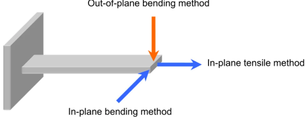
specimen design, and equipment. However, there are no standard test methods so far. Among these test methods of approaches, tensile and bending tests are two common schemes for the fatigue characterization on micrometer-scale specimens. And the microsized cantilever-beam is utilized frequently in specimen design. As shown in Figure 1.3, according to loading methods on the free end of the cantilever-beam, three fatigue test types can be identified: (1) in-plan tensile method, (2) in-plane bending method, and (3) out-of-plane bending method.
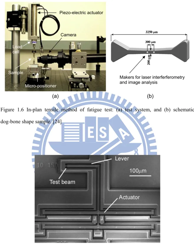
For the in-plan tensile method, in 2003, Cho et al. [22] used microsample tensile machine and non-contact interferometer strain displacement gage to study the fatigue properties of electrodeposited LIGA Ni microsamples (~400 μm thick) with dog-bone shape under the test frequency of 200 Hz, as shown in Figure 1.4. The test results indicated that the fatigue lifetime of the LIGA Ni microsamples increased with decreasing stress amplitude, and the measured fatigue limit and endurance ratio were 195 MPa and 0.35, respectively. In 2004, Son et al. [23] evaluated and discussed the fatigue properties and notch effect of LIGA Ni film (10 μm thick) by micro-tensile and fatigue test methods under the test frequency of 20 Hz, as shown in Figure 1.5. The test results indicated that the fatigue strength of LIGA Ni was very sensitive to stress concentration, and the measured fatigue limit and endurance ratio were 180 MPa and 0.21 for unnotched specimens, and 143 MPa and 0.17 for notched specimens, respectively. In 2007, Yang et al. [24] also used the micro-tensile testing system to study the fatigue mechanisms of LIGA Ni thin films (70 μm and 270 μm thick) with micro-scale and nano-scale grains under the test frequency of 10 Hz, as shown in Figure 1.6. The test results indicated that films with the nano-scale grains (15 nm average grain size) were shown to have higher strength and fatigue resistance than those with micro-scale columnar grain structures (5 μm wide and 5 ~ 25 μm long). The thinner films (70 μm thick with a columnar microstructure) were also
shown to have higher strength and fatigue resistance than those of thicker films (270 μm thick with a columnar microstructure).
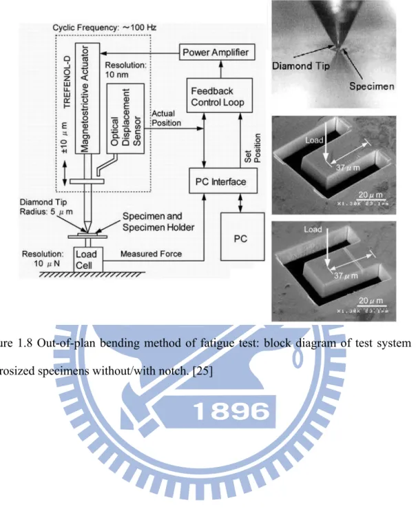
For the in-plan bending method, in 2003, Larsen et al. [15] proposed an in situ bending test device with integrated electrostatic actuator and test beam, made of electroplated nanocrystalline Ni (7 μm thick), for fatigue investigation under the test frequency of 200 Hz, as shown in Figure 1.7. The feature of this test device was approximately pure in-plane bending, and the maximum stresses were calculated using finite element method. The test results indicated that the nanocrystalline Ni had good fatigue properties due to the high strength and toughness of nanocrystalline material. However, the clear fatigue limit and endurance ratio were not obtained in this study.
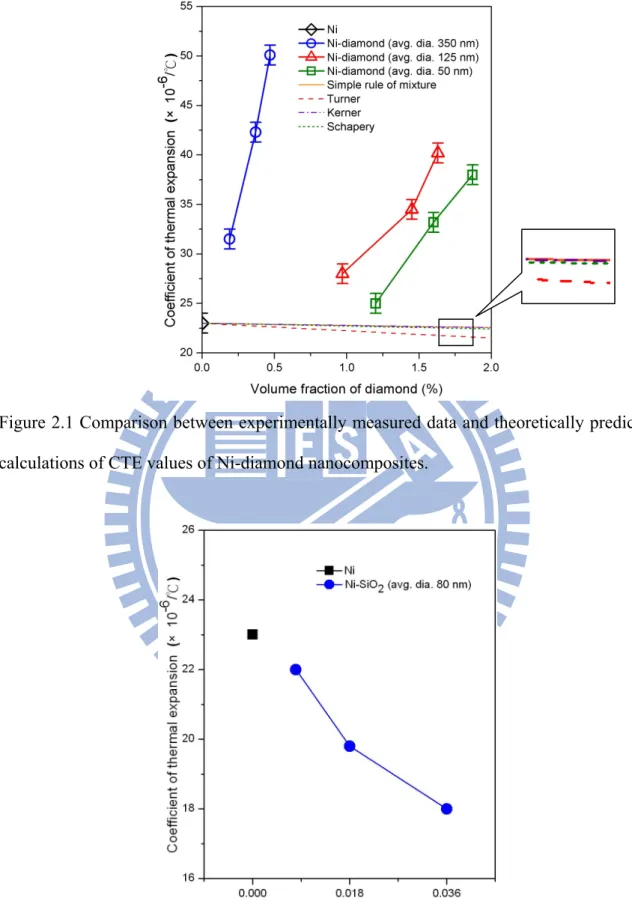
For the out-of-plan bending method, in 1999, Maekawa [25] et al. performed fatigue lifetime and fatigue crack propagation tests on electroless plated Ni-P amorphous alloy specimen (12 μm thick) to investigate the material fatigue properties under the test frequency of 10 Hz, as shown in Figure 1.8. The microsized specimens were cantilever-beam-type prepared by focused ion beam (FIB) machining, and notches with a depth of 3 μm were introduced in some specimens. The fatigue lifetime curve was obtained for unnotched specimens, and the fatigue crack propagation tests were performed using notched specimens. The test results indicated that the crack was deduced to propagate by cyclic plastic deformation at the crack tip even in microsized amorphous alloys, and the measured fatigue limit and endurance ratio were 20 mN and 0.43, respectively.
From above reviews, we can find that once the sample becomes very small only with several micrometers, the setup of tensile method become stringent to grip, align, and pull a tested sample. In comparison with the tensile method, the bending method can be free of the issues raised by sample gripping and alignment. Furthermore, bending method
requires smaller loading force than that of tensile tests to yield a tested sample with a deformation that is large enough for accurate measurement, which makes the method suitable for thin film characterization. Thus, in this dissertation, a fatigue characterization scheme based on the design of out-of-plane bending method is proposed and utilized for the property investigations on the electroplated Ni and Ni-diamond nanocomposite.
1.3 Dissertation Outline
The goal of this dissertation is to investigate CTE and fatigue properties of electroplated Ni and Ni-diamond nanocomposite in terms of CTE variation mechanism, material application, and reliability issue. The detailed study including fabrication and measurement methods, experimental results, and characterizations are described in the following chapters.
In Chapter 2, the promising factor is proposed to explain the CTE variation by using the XRD investigation on electroplated Ni-based nanocomposites with different nano-particle types (i.e. diamond and SiO2).
In Chapter 3, the application of CTE property on bimorph effect is investigated by Ni/Ni-diamond nanocomposite, and a newly Ni-based thermal bimaterial structure for sensor and actuator application is also proposed.
In Chapter 4, a fatigue characterization scheme based on the bending-test design is proposed and utilized for the property investigations on the electroplated Ni and Ni-diamond nanocomposite (incorporated with two different particle sizes, i.e. 350 nm and 50 nm in diameter) in terms of Young’s modulus, fatigue lifetime, fatigue strength, and fracture mechanism.
Finally, Chapter 5 concludes this dissertation and suggests the future research direction.
Figure 1.1 Mechanism of particles co-deposition into a metal deposit. [7]
Figure 1.2 Fatigue test apparatus for making rotating-bending test. [21]
- + Specimen Load Load High-speed motor Counter 1084139
Figure 1.3 Common fatigue test types classified by loading methods.
Figure 1.4 In-plan tensile method of fatigue test: test machine and specimen. [22]
Figure 1.5 In-plan tensile method of fatigue test: (a) test system, and (b) schematic diagram of specimen. [23]
In-plane tensile method Out-of-plane bending method
In-plane bending method
Figure 1.6 In-plan tensile method of fatigue test: (a) test system, and (b) schematic dog-bone shape sample. [24]
Figure 1.7 In-plan bending method of fatigue test: fatigue test device integrated with test beam and electrostatic actuator. [15]
Load cell Piezo-electric actuator Camera Sample Micro-positioner (a) (b)
Makers for laser interferferometry and image analysis
Figure 1.8 Out-of-plan bending method of fatigue test: block diagram of test system and microsized specimens without/with notch. [25]
Chapter 2 Investigation on CTE Property
2.1 Introduction
In the previous investigation, our group, Tsai et al. [12, 13] found that the electro-thermal microactuator made of Ni-diamond can reduce 73% power requirement comparing with the electroplated Ni one for the same output displacement of 3 μm, and can enlarge the reversible displacement range from 1.8 μm to 3 μm (i.e. more than 67% ultimate elongation), simultaneously. These performance enhancements were resulted by the augment of CTE of Ni via the nano-diamond particles incorporation. However, such a CTE enhancement does not follow the rule of mixtures (ROMs) in metal matrix composites (MMCs). There must be some factor that affects the CTE variation via the incorporated nano-diamond particles in the Ni-diamond nanocomposite.
In this study, referring to the past literatures and employing the XRD investigation, the promising factor is proposed to explain the CTE variation on electroplated Ni-based nanocomposites with different nano-particle types (i.e. diamond and SiO2).
2.1.1 Rule of Mixtures
ROMs are the common function to predict the CTE of MMCs. In general, the CTE of MMCs is usually assumed to follow a simple ROMs dependence on volume fractions of presence phases, known as the linear ROMs [26, 27]:
p p m m c V α V α α = + (2.1)
where α is the CTE and V is the volume fraction. The subscripts of c, m, and p
denote composite, matrix phase, and particle phase, respectively. In fact, the CTE of MMCs is hard to be predicted only using the linear ROMs because it is affected by several factors such as reinforcement volume fraction, fabrication process, and the nature of the
composite constituents [28]. For the linear ROMs, it assumes the composite is a simple mixture of two phases with each phase exhibiting physical behaviors that are not influenced by their presence in mixture, and therefore the effects of microstructure, plasticity, and thermal softening are not account for. To improve the accuracy of the linear ROMs, several models have been proposed for predicting the CTE of MMCs. Among these, the most often mentioned and used are Turner [29], Kerner [30], and Schapery [31] models. To begin with the Turner’s model, it assumes homogeneous strain throughout the composite and uses a balance of internal average stresses. By considering that the sum of the internal forces equals to zero, the CTE of MMC is obtained:
m m p p m m m p p p c K V K V K V K V + + =α α α (2.2)
where K is the bulk modulus which calculated using the standard relationship of Young’s
modulus (E ) and Poisson's ratio (υ ):K = E/3(1−2υ). Next, the Kerner’s model assumes that the particle is spherical and clothed by a uniform layer of matrix. By considering that the composite is the volume element, the CTE of MMC becomes:
) 4 / 3 ( ) 1 ( ) )( )( 1 ( m m p p p m p m p m p p p c G K K K V K V K K V V + + − − − − + =α α α α (2.3)
where α is the linear ROMs CTE as expressed in Equation 2.1 and G is the shear modulus which calculated using the standard relationship of Young’s modulus and Poisson's ratio:G= E/2(1+υ). Lastly, the Schapery’s model has been developed by considering the thermoelasticity based on extremum principles for predicting the CTE of isotropic composites. The CTE of MMCs can be expressed as the following equation:
⎥ ⎥ ⎦ ⎤ ⎢ ⎢ ⎣ ⎡ − − − + = p m p c p m p c K K K K / 1 / 1 / 1 / 1 ) (α α α α (2.4)
of α , E , and υ used for computing the predicted CTE of Ni-diamond nanocomposite by Equations 2.1 ~ 2.4 are extracted from previous experiment work [12, 13, 21, 33] that the Young’s modulus of pure electroplated Ni is measured by means of a nanoindentation test, the CTE value of Ni-based nanocomposite is measured by calculating the elongation-temperature ratio of Ni-based microcantilever beam during the temperature range from room temperature (~25 °C) to 400 °C, and the weight fraction of diamond in nanocomposite is measured by the elemental analyzer (EA). As shown in Figure 2.1, the computing results of the predicted CTE of Ni-diamond nanocomposite using Equations 2.1 ~ 2.4 are plotted.
Figure 2.1, compares the CTE values of Ni-diamond nanocomposites between experimentally measured data and theoretically predicted calculations in the range of 0% ~ 2% volume fraction of diamond. It shows that the experimental CTE values of Ni-diamond nanocomposites, which don’t follow the theoretical ROMs, are higher than that of theoretical predictions and the matrix material of pure electroplated Ni (23 ×10-6/°C, as measured). Furthermore, the experimental CTE values of Ni-diamond nanocomposites increase with the volume fraction and the particle size of nano-diamond. For the nanocomposites plated in a bath with an average diameter of 350 nm nano-diamonds, the CTE values increase from 31.5 ×10⁻⁶/°C to 50.1 ×10⁻⁶/°C while the volume fraction increase from 0.19% to 0.47%. With the size enlargement of nano-diamond particles, the CTE values are found to increase from 38.0 ×10⁻⁶/°C of the composite synthesized with an average diameter of 50 nm nano-diamonds up to 50.1 ×10⁻⁶/°C of that with an average diameter of 350 nm nano-diamonds.
2.1.2 Particle Effect
In order to investigate the particle effect on CTE of Ni-based nanocomposite [13], electroplated Ni-SiO2 nanocomposite is prepared by adding SiO2 nanoparticles with an average diameter of 80 nm into Ni plating bath. As shown in Table 2.1, the plating conditions of pH values and temperatures are maintained at 4.1 ~ 4.3 and 50 °C, and the concentration of the SiO2 nanoparticles are ranging from 0 g/L to 0.036 g/L which are determined by the same volume fraction of nanoparticles inside Ni plating bath as nano-diamonds. In Figure 2.2, the measured CTE values of Ni-SiO2 nanocomposites with different particle concentration are obtained by calculating the elongation-temperature ratio of Ni-SiO2 microcantilever beams during the temperature range from room temperature to 400 °C. The measured results show that the added SiO2 nanoparticles will diminish the CTE values of electroplated composites, and the nanocomposite of Ni-SiO2 has opposite CTE performance from Ni-diamond. In our experiment results of Ni-SiO2 nanocomposites, the CTE values are found to decrease from 22 ×10-6/°C to 18 ×10-6/°C with the augment of SiO2 nanoparticles concentration in plating bath from 0.008 g/L to 0.036 g/L.
From the preliminary investigation of particle effect, up to now, the CTE enhancements of Ni are attributed to the incorporation of nano-diamond particles. As mentioned before, however, such a CTE enhancement can’t be explained by the ROMs of MMCs in Equations 2.1 ~ 2.4. There must be some factors, which affect CTE property of Ni-diamond nanocomposite, needing further investigation.
2.1.3 Factors that Affect CTE
From the literature survey, the related research of CTE enhancement is limited and only can be found in pure material. In these limited researches, the factors that affect
CTE enhancement can be attributed to crystalline grain size [34, 35] and stress modes including microstress (ex. microstrain [36]) and macrostress (ex. pre-stressing [37, 38] and residual stress [39]).
For the factor of crystalline grain size, in 1989, Birringer [34] found that the CTE of nanocrystalline Cu (grain size ~8 nm) was about 1.94 times than that of conventional polycrystalline counterpart. In 1995, Lu and Sui [35] found that the CTE of porosity-free nanocrystalline Ni-P (grain size <127 nm) increased with the reduction of crystalline grain size.
For the factor of microstress, in 2002, Qian et al. [36] found that the CTE of nanocrystalline Cu increased by about 12% with an increment of the microstrain from 0.14% to 0.24% which was conducted by quantitative XRD measurements. In addition, the microstrain effect on thermal properties in the nanocrystalline Cu might be attributed to the change in density of grain boundary defects/dislocations.
For the factor of macrostress in pre-stressing, in 1970, Gazda [37] found that a compressive pre-stressing caused the CTE of graphite to increase and that annealing caused the CTE to decrease toward the original value. As expected, the 90% compression samples gave the largest changes in CTE. It was also interesting to note that the increase in CTE appeared to be independent of particle size, but dependent on the grain orientation. In addition, the CTE resulted in the direction perpendicular to the compression gave very slight CTE increase. In 1971, Hart [38] found that uniaxial compressive loading resulted in an increase in CTE of graphite, but tensile loading caused an opposite effect. This result can be explained by the crack closure model [40] which is used to explain graphite thermal expansion accommodation. In the present work, uniaxial compression caused an increase in specimen density and a corresponding increase in thermal expansion. This suggested that cracks which initially contributed to accommodation were closed under
compressive loading modes. On the other hand, tensile pre-stressing reduced density (i.e. opened additional cracks) and reduced thermal expansion. In addition, this research was also shown that all loading mode caused a decrease in the Young’s modulus due to the increased dislocation density and cracking induced by pre-stressing.
For the factor of macrostress in residual stress, in 2000, Fang and Lo [39] found that the CTE of the Al thin film increased from 18.23 ×10⁻⁶/°C to 29.97 ×10⁻⁶/°C as the film thickness increased from 0.3 μm to 1.7 μm under residual compressive stress. Oppositely, the CTE of the Ti thin film decreased from 21.21 ×10⁻⁶/°C to 9.04 ×10⁻⁶/°C as the film thickness increased from 0.1 μm to 0.3 μm under residual tensile stress.
From above researches, in order to further discuss the effects of crystalline grain size and stress mode on the CTE property of Ni-based nanocomposite, the following XRD investigation will be performed.
2.2 Measurements and Discussions
2.2.1 Grain Size Measurement
As shown in Figure 2.3, the XRD patterns of as-fabricated pure Ni, Ni-diamond (average particle size: 350 nm; particle concentration: 2 g/L), and Ni-SiO2 (average particle size: 80 nm; particle concentration: 0.036 g/L) nanocomposites are measured by the X-ray diffractometer (PANalytical X'Pert Pro MRD) using θ −2θ scan with Cu-Kα radiation (i.e. wave length λ =1.5405 Å). In Figure 2.3, the face-centered-cubic (FCC) texture of electroplated pure Ni, Ni-diamond, and Ni-SiO2 nanocomposites have been observed with the preferred orientation of (111). Therefore, in this study, the diffraction peak (111) is chosen for the calculation of crystalline grain size, and the crystalline grain size is estimated according to the Scherrer’s formula [41]:
θ β λ cos 9 . 0 = D (2.5)
where λ is the wave length, β is the full width at half maximum (FWHM), and θ is the diffraction angle which is half of the peak centroid.
By the commercial analysis software (MDI Jade 5.0), the related parameters of Equation 2.5 can be derived from the XRD data (i.e. Figure 2.3) as shown in Table 2.2. The calculated results show that the crystalline grain sizes of electroplated Ni, Ni-diamond, and Ni-SiO2 nanocomposites are 20.5 nm, 20.0 nm, and 21.6 nm, respectively. It is noted that these grain sizes are similar to each other in nanometer size. There is no dramatically size variation from micro-scale to nano-scale. Thus, the effect of crystalline grain size can be eliminated from the factors that affect CTE.
2.2.2 Stress Mode Investigation
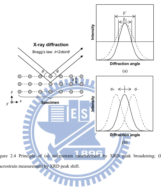
For the investigation on stress mode, as shown in Figure 2.4, the measurement of microstrain (for microstress) and macrostrain (for macrostress) are performed by the XRD peak broadening and peak shift, respectively, which are based on Bragg’s law as follows [41-44]:
θ
λ =2dsin (2.6)
where λ is the wave length, d is the spacing of the diffraction plane, and θ is the diffraction angle. The microstrain is determined by the XRD peak broadening (i.e. the change of FWHM) as follows [41, 42]: θ β ε tan 4 Δ = micro (2.7)
Comparing between Equation 2.5 and Equation 2.7, it can be found that the change of FWHM (β) depends on crystalline grain size (D ). As mentioned before, thus, the effect
of microstress can also be eliminated from the factors that affect CTE.
From Equation 2.6, it can be found that if an additional force yields a lattice spacing reduction (i.e. compressive strain), the position of XRD peak (i.e. diffraction angle) will
shift toward a higher angle On the contrary, the yielded expansion of lattice spacing (i.e. tensile strain) will cause peak position shift toward a lower angle. Therefore, the macrostrain can be determined by the XRD peak shift (i.e. the change of lattice spacing) as follows [41, 43, 44]: 0 0 0 ' d d d d d macro Δ = − = ε (2.8)
where d0 is the lattice spacing of stress-free material and d' is the lattice spacing for strained material. From the Equation 2.6 and XRD data of Figure 2.3, the spacing values of electroplated Ni, Ni-diamond, and Ni-SiO2 nanocomposites can be determined as shown in Table 2.2. Based on the pure electroplated Ni, the macrostrains of Ni-diamond and Ni-SiO2 nanocomposites can be determined as -0.15% and 0.09%, respectively. It is noted that the incorporation of nano-diamond particles in Ni matrix causes compressive strain in nanocomposite, and the incorporation of SiO2 nano-particles in Ni causes tensile strain in nanocomposite.
Combining with the experimental CTE data, Ni-diamond nanocomposite with compressive stress inside is observed to have higher CTE value than that of pure electroplated Ni. As opposed to Ni-diamond nanocomposite, Ni-SiO2 nanocomposite with tensile stress inside is observed to have lower CTE value than that of pure electroplated Ni. Therefore, from the previous literature review, the factor of macrostress effect may be the main reason which causes the CTE variation on Ni-based nanocomposites.
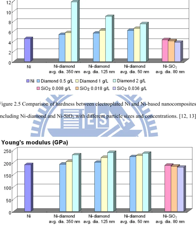
In this dissertation, this stress difference between Ni-diamond and Ni-SiO2 nanocomposites is though coming from the fabrication process, so-call residual stress, according to the hardness or Young’s modulus difference between Ni matrix and nanoparticles. From the hardness and Young’s modulus measurement of electroplated pure Ni, Ni-diamond, and Ni-SiO2 nanocomposites [12, 13] as shown in Figures 2.5 and
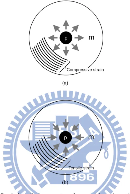
2.6 respectively, it can be found that Ni matrix incorporated with higher hardness and Young’s modulus of diamond particles conducts higher hardness and Young’s modulus of Ni-diamond nanocomposite than that of electroplated pure Ni due to the simple rule of mixtures [21]. Oppositely, Ni matrix incorporated with lower hardness and Young’s modulus of SiO2 particles conducts lower hardness and Young’s modulus of Ni-SiO2 nanocomposite than that of electroplated pure Ni. Therefore, during co-electrodeposited process of Ni-diamond nanocomposite, diamond particles will construct a compressive stress to Ni matrix due to its higher hardness and Young’s modulus than that of Ni matrix, as shown in Figure 2.7(a). On the contrary, for Ni-SiO2 nanocomposite as shown in Figure 2.7(b), the hardness and Young’s modulus of SiO2 particles are lower than that of Ni matrix so that SiO2 particles will construct a tensile stress to Ni matrix during co-electrodeposited process.
2.3 Summary
Through the XRD investigation on peak shift, residual stresses types of Ni-based nanocomposites compared with pure electroplated Ni can be determined. These residual stresses, which are constructed from co-electrodeposited process due to the hardness or Young’s modulus difference between matrix and particles, are thought as the promising factor to affect the CTE variations in nanocomposites. For Ni-diamond nanocomposite, the measured result shows that the incorporated nano-diamond particles (average particle size: 350 nm; particle concentration: 2 g/L) will enhance the CTE of electroplated Ni from 23 ×10-6/°C to 50.1 ×10⁻⁶/°C with residual compressive stress (0.15% compressive strain). Oppositely, for Ni-SiO2 nanocomposite, the measured result shows that the incorporated nano-SiO2 particles (average particle size: 80 nm; particle concentration: 0.036 g/L) will diminish the CTE of electroplated Ni from 23 ×10-6/°C to 18 ×10-6/°C with residual tensile
stress (0.09% tensile strain). Therefore, employing a simple composite-plating process, material properties including CTE, Young’s modulus, and hardness can be modified easily in the expected way. This work has provided an alternative material selection for the development of MEMS devices with optimum properties using nanocomposites.
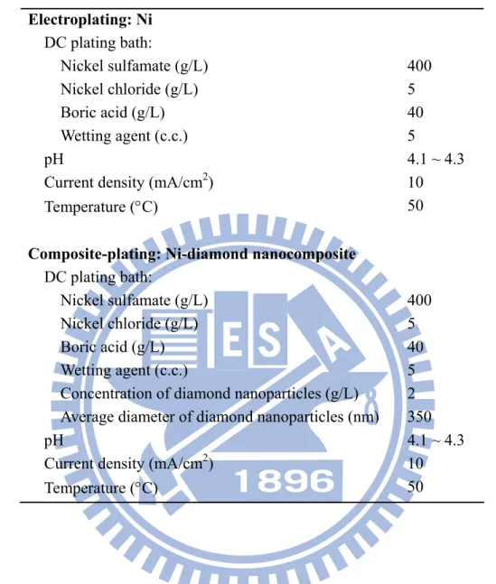
Table 2.1 Plating bath conditions of Ni-based nanocomposites. Ni-diamond nanocomposite DC plating bath: Nickel sulfamate (g/L) 400 Nickel chloride (g/L) 5 Boric acid (g/L) 40 Wetting agent (c.c.) 5
Concentration of diamond nanoparticles (g/L) 0.5, 1, 2 Average diameter of diamond nanoparticles (nm) 50, 125, 350
pH 4.1 ~ 4.3
Current density (mA/cm2) 10
Temperature (°C) 50 Ni-SiO2 nanocomposite DC plating bath: Nickel sulfamate (g/L) 400 Nickel chloride (g/L) 5 Boric acid (g/L) 40 Wetting agent (c.c.) 5
Concentration of SiO2 nanoparticles (g/L) 0.008, 0.018, 0.036 Average diameter of SiO2 nanoparticles (nm) 80
pH 4.1 ~ 4.3
Current density (mA/cm2) 10
Temperature (°C) 50
Table 2.2 Parameters derived from XRD investigation on Ni-based nanocomposite. 2θ (°) β (°) D (nm) d (Å) εmacro (%)
* Ni-diamond nanocomposite 44.569 0.440 20.0 2.0313 -0.15 Pure electroplated Ni 44.498 0.431 20.5 2.0344 ---
† Ni-SiO
2 nanocomposite 44.455 0.409 21.6 2.0362 0.09
* The average diameter and contraction of adding nano-diamond particles in plating bath are 350 nm and 2 g/L.
* The volume fraction of diamond in nanocomposite is 0.47%. † The average diameter and contraction of adding SiO
2 nanoparticles in plating bath are 80 nm and 0.036 g/L.
Figure 2.1 Comparison between experimentally measured data and theoretically predicted calculations of CTE values of Ni-diamond nanocomposites.
Figure 2.2 Comparison of CTE properties between pure electroplated Ni and Ni-SiO2 nanocomposites with different particle concentration. [13]
Figure 2.3 The XRD patterns at room temperature for the as-fabricated pure Ni, Ni-diamond (average particle size: 350 nm; particle concentration: 2 g/L), and Ni-SiO2 (average particle size: 80 nm; particle concentration: 0.036 g/L) nanocomposites.
Figure 2.4 Principle of (a) microstrain measurement by XRD peak broadening; (b) macrostrain measurement by XRD peak shift.
d θ
θ
Bragg’s law: λ=2dsinθ X-ray diffraction Specimen z x y Diffraction angle Intensity d− d+ (b) Diffraction angle Intensity β0 β’ (a)
Figure 2.5 Comparison of hardness between electroplated Ni and Ni-based nanocomposites including Ni-diamond and Ni-SiO2 with different particle sizes and concentrations. [12, 13]
Figure 2.6 Comparison of Young’s moduli between electroplated Ni and Ni-based nanocomposites including Ni-diamond and Ni-SiO2 with different particle sizes and concentrations. [12, 13]
Figure 2.7 Resulted residual stress type from particle and matrix in Ni-based nanocomposite: (a) compressive stress in Ni-diamond; (b) tensile stress in Ni-SiO2.
(b)
m
p Tensile strain (a) pm
Compressive strainChapter 3 Application of CTE Property on Bimorph Effect
3.1 Introduction
Bimaterial structure can provide thermally-bended deformation due to the CTE mismatch between two bonded materials, so-called bimorph effect [45, 46]. Upon this effect, the bimaterial structure based transducers can detect external stimulus of temperature change and provide temperature-driven output force simultaneously. To date, thermal bimaterial structure has been widely utilized in several MEMS devices, such as thermal sensor [47], stress sensor [48], biological sensor [49], microvalve [50], pumping membrane [51], tilting micromirror [52], microrelay [53], microswitch [54], etc. Nevertheless, thermal bimaterial structure typically will exhibit initial deformation once the structure is released. This deformation is resulted by the residual thermal stress [55-57] induced in structural fabrication where structural materials have different CTE and process temperatures. Delaminating is also a common issue that may happen on the interlamination through large residual stress and low cohesive energy [58-60] to reduce the lifetime and reliability of thermal bimaterial structure. For a bimaterial structure, by arranging the low-CTE layer on top, thermal upward actuation can be achieved [61, 62]. However, since metal usually has higher CTE comparing to nonmetal material, thermal upward actuation is difficult to achieve when the metal layer is deposited above the nonmetal layer [52-54, 57]. Thus, further investigations in terms of material and process selection and structure design are still required for future applications of thermal bimaterial structure.
In recent researches, Teh et al. found that the incorporation of nano-diamonds in electrolytic Ni matrix to form Ni-diamond nanocomposite could reduce the film residual stress and render the film more compressively [20]. Besides, the nanocomposite could
exhibit a higher CTE than that of electroplated Ni [12, 13]. Therefore, this study will investigate the bimorph effect of Ni/Ni-diamond nanocomposite bimaterial and propose a newly thermal bimaterial microactuator by employing the advantages of Ni-diamond nanocomposite. It is our belief that the proposed thermal device using the Ni/Ni-diamond nanocomposite bimaterial would have better interfacial bonding strength and smaller residual thermal stress since Ni and Ni-diamond nanocomposite have different CTE but similar crystal structure and process temperature. By controlling the plating sequence of Ni and Ni-diamond nanocomposite, the fabricated thermal bimaterial structure desired to have upward or downward bended deformation can also be easily achieved.
3.2 Bimaterial Structure Design
Figure 3.1 shows the scheme of thermal bimaterial structures made of Ni/Ni-diamond nanocomposite bimaterial including upward and downward deflection types for bimorph effect investigation. Upon the plating sequence of Ni and Ni-diamond nanocomposite, two deflection types of thermal bimaterial structures, including upward and downward types, are available. The designed length L of fabricated thermal bimaterial structure ranged from 200 μm to 1500 μm where the width w is fixed at 50 μm. The connecting beam is 50 μm long (Lc) and 30 μm wide (wc). The thickness of Ni and Ni-diamond nanocomposite layers are determined according to the optimum thermomechanical sensitivity ST defined as tip deflection d for a temperature change TΔ .
T d ST
Δ
= (3.1)
where d and following F are the thermally generated tip deflection and the output force of a thermal bimaterial structure, respectively. The deflection and force can be expressed by the following equations [45]:
) 2 3 2 ( 2 ) ( ) ( ) )( ( 3 2 2 2 1 2 1 2 1 2 1 2 1 2 2 2 2 2 2 2 1 1 1 2 2 1 2 1 2 1 2 1 2 1 t t t t t t E E w w t E w t E w TL t t t t E E w w d + + + + Δ − + = α α (3.2) and Kd L d EI F =3 3 = (3.3)
where E , i αi, w , and i t ( i =1, 2) are, respectively, Young’s modulus, CTE, width, and i
thickness of each layer; L , EI , and K are, respectively, the length, flexural rigidity and
spring constant of thermal bimaterial structure, and TΔ is the temperature change.
A folded structure design is introduced into the thermal bimaterial structure to increase output force and to decrease the thermal vibrational noise. For thermal bimaterial structure, the amount of tip deflection is proportional to the square of the structure length as shown in Equation 3.2, so the thermal bimaterial structure becomes more sensitive with increased length of bimaterial structure as shown in Equation 3.1. However, lower spring constant resulting from an increased length also decreases the output force as shown in Equation 3.3 and increases the thermal vibrational noise as follows [47]: fQ K TB k dn = 2 B / π (3.4)
where kB is the Boltzmann constant, T is the absolute temperature, B is the measurement bandwidth, K is the cantilever spring constant, f is the resonance
frequency, and Q is the quality factor of the resonance. Since a folded structure
behaves like the structure of two beams connected in parallel which can have a higher spring constant due to larger width, a promising way to increase output force and sensitivity of the thermal bimaterial structure without a significant increase of the thermal vibrational noise is to connect multiple bimaterial cantilever beams in a folded manner.
Before the layer thickness determination of thermal bimaterial structure, cantilevers made of single layer of Ni and Ni-diamond nanocomposite are first fabricated to
characterize the CTE of material and to measure CTE mismatch. By measuring the elongation of cantilever in a heated chamber with temperature control, CTE of Ni and Ni-diamond nanocomposite are found to be 15.6 ×10⁻⁶/°C and 19.4 ×10⁻⁶/°C, respectively, where the diamond content of the corresponding nanocomposite film is 0.32% in weight fraction according to the EA measurement. The Young’s modulus of the electroplated film is characterized by the nanoindenter (MTS Nano Indentor XP) [63]. The indentation depth is set as 1/10 film thickness, and the measured value is the average over twenty test points. The measured Young’s moduli of Ni and Ni-diamond nanocomposite by means of a nanoindentation test are found to be 211.0 GPa and 224.1 GPa, respectively.
Based on Equation 3.1, Equation 3.2 and aforementioned material properties, for the upward type thermal bimaterial structure with L =1500 μm and w=50 μm, the calculated thermomechanical sensitivity as function of Ni layer thickness is shown in Figure 3.2, respectively. Then, the optimal Ni thickness t2 is found to be around half of the Ni-diamond nanocomposite thickness t1 for the maximum themomechanical sensitivity [64]. For instance, for a bimaterial with the structure of 3 μm thick Ni and 6 μm thick Ni-diamond nanocomposite, the themomechanical sensitivity can be designed as high as 640.2 nm/K with the flexural rigidity of 6.61×10⁻¹⁰ N⋅m2, and the output force of 150.5 μN as Δ =200 °C. Similarly, for downward type thermal bimaterial structure, the layer T
thickness of Ni and Ni-diamond nanocomposite are also determined to be 3 μm and 6 μm respectively.
3.3 Bimaterial Structure Fabrication
Figure 3.3 depicts the fabrication process of the proposed thermal bimaterial structure. Initially, the 0.5 μm thick SiO2 on a silicon wafer with patterned etching windows is first coated with 5 μm thick AZP-4620 photoresist (PR) and patterned as sacrificial layer
(Figure 3.3(a)) After hard baking, it is followed by sputtering seed layer of 1000 Å Cu onto 200 Å Ti as adhesion layer. 15 μm thick AZP-4620 PR is then spin coated and patterned to form the plating mold of thermal bimaterial structure, as shown in Figure 3.3(b). For upward type thermal bimaterial structure, the 6 μm thick composite-plating of Ni-diamond layer is deposited first to construct the bottom layer of thermal bimaterial structure. Subsequently, 3 μm thick electroplated Ni is deposited to construct the top layer (Figure 3.3(c)). Table 3.1 shows the plating bath condition, and the plating temperatures of both layers are kept at 50 °C. For the composite-plating of Ni-diamond nanocomposite which is different from electroplated Ni, the nano-diamond particles with 350 nm in average diameter are added into a sulfuric based Ni plating bath for the co-deposition, and the concentration of the nano-diamond particles in plating bath is 2 g/L. Finally, the fabricated thermal bimaterial structure is released after stripping the sacrificial layer by acetone solution (Figure 3.3(d)), and the silicon underneath is removed by KOH solution (Figure 3.3(e)). For downward type thermal bimaterial structure, the fabrication process is similar to the upward one except switching the plating sequence of Ni-diamond nanocomposite and Ni in Figure 3.3(c). By controlling the plating sequence of Ni and Ni-diamond nanocomposite, two deflection types of thermal bimaterial structures including upward and downward are easily fabricated.
Figures 3.4(a) and 3.4(b) show the scanning electron microscope (SEM) pictures of the upward and downward types of fabricated thermal bimaterial structures. It is found that no initial deformation is observed as proposed due to the same low process temperature of electroplated Ni and Ni-diamond nanocomposite for lower residual thermal stress in thermal bimaterial structure.
3.4 Measurements and Discussions
3.4.1 Thermal Performance Measurement
Figure 3.5 illustrates the set-up for the thermal performance measurement of the fabricated thermal bimaterial structure in terms of tip deflection in thermal chamber. First, a chip with thermal bimaterial structure is placed on a heating system in a chamber with temperature controller, and the focused tip image of thermal bimaterial structure is captured by a charge-coupled device (CCD) through optical microscope with positional z-adjustment. As the thermal bimaterial structure is heated up, the structural tip will deflect and result in a focus change, which requires z-adjustment to search for a new focus to have a clear tip image. Thus, the micrometer-scale tip deflection of thermal bimaterial structure is determined by measuring the focus variation ( ZΔ ) and the measurement accuracy of Δ is about 0.5 μm on positional z-adjustment. The measured out-of-plane Z
tip deflections of fabricated thermal bimaterial structures including upward and downward types with length of 800 μm, 1000 μm, and 1500 μm are observed with temperature change from 0 °C to 200 °C. The relationship between tip deflection and elevated temperature is plotted in Figures 3.6(a) and 3.6(b). According to the measured results of thermal performance, as structure length L =1500 μm and temperature change TΔ =200 °C, the measured tip displacement of upward and downward types can reach around 82.5 μm and -22.5 μm, respectively. In this condition, the themomechanical sensitivity and output force are calculated, respectively, to be 412.5 nm/K and 97.0 μN for upward type thermal bimaterial structure; and -112.5 nm/K and -26.5 μN for downward type one.
From above calculated results of upward type thermal bimaterial structure, the thermomechanical sensitivity and output force are smaller than the theoretical calculation; and the thermal performance in tip deflection of downward type is not as large as upward type. It seems that the CTE difference between Ni and Ni-diamond nanocomposite in the
thermal bimaterial structure is not equal to the cantilevers’ that made of single material layer. Assuming material properties of bottom structural layers of thermal bimaterial structure are the same as cantilever’s that made of single Ni or Ni-diamond nanocomposite layer. Using Equation 3.2 and the measured data of Figures 3.6(a) and 3.6(b), the CTE of the top structural layer of thermal bimaterial structure have been modified to fit the experiment data. Therefore, as shown in Table 3.2, the CTE of top structural layer of Ni in upward type is modified to be 16.9 ×10⁻⁶/°C which is 8.3% deviation from single Ni cantilever. Similarly, the CTE of top structural layer of Ni-diamond nanocomposite in downward type is modified to be 16.2 ×10⁻⁶/°C which is 16.5% deviation from single Ni-diamond nanocomposite cantilever.
Seed layer effect may be the major cause resulting in the aforementioned CTE variation. While Ni-diamond nanocomposite is used as the top structural layer of thermal bimaterial structure in downward type, the plating seed layer of Ni-diamond nanocomposite is a 3 μm thick electroplated Ni. On the contrary, as Ni-diamond nanocomposite is used as the bottom structural layer in upward type, the plating seed layer is 1000 Å sputtering Cu which is similar to single material cantilever. According to atomic force microscope (AFM) surface images of 6 μm Ni-diamond nanocomposite on 3 μm electroplated Ni and 1000 Å sputtered Cu seed layers as shown in Figures 3.7(a) and 3.7(b), respectively, the Ni-diamond nanocomposite electroplated on the Ni layer has a higher surface roughness value (Ra) than that on the sputtering Cu layer. The rougher surface could be attributed to the difference of grain structure of Ni-diamond nanocomposite that may vary with the different seed layers and so does the material property of CTE. Further material characterization is required for verification.