I
國 立 交 通 大 學
光電工程研究所碩士班
碩士論文
非晶銦鎵鋅氧化物薄膜電晶體之背通道調製效應
Back Interface Engineering of Amorphous
In-Ga-Zn-O Thin Film Transistor
研究生: 葉雋正
指導教授:冉曉雯 教授
蔡娟娟 教授
II
Back Interface Engineering of Amorphous
In-Ga-Zn-O Thin Film Transistor
研究生: 葉雋正
Student:Chun-Cheng Yeh
指導教授:冉曉雯 教授 Advisor:Prof. Hsiao-Wen Zan
蔡娟娟 教授 Prof. Chuang-Chuang Tsai
國立交通大學 光電工程研究所碩士班
碩士論文
A Thesis
Submitted to Electro-Optical Engineering
College of Electrical Engineering and Computer Science National Chiao Tung University
in partial Fulfillment of Requirements for the Degree of Master
in
Electro-Optical Engineering July 2011
Hsinchu, Taiwan, Republic of Chin
III
非晶銦鎵鋅氧化物薄膜電晶體之背通道調製效應
研究生:葉雋正 指導教授:冉曉雯 教授
蔡娟娟 教授
國立交通大學
光電工程究所碩士班
中文摘要
非晶銦鎵鋅氧化物半導體(a-IGZO)所構成的薄膜電晶體,可在低溫製程(常溫濺鍍) 成膜,並具有高於非晶矽薄膜電晶體(a-Si:H TFT)的電子遷移率(>10cm2 /VS),故在顯示 科技領域上具有很大運用潛力。此外由於 IGZO 在大氣環境下非常穩定,複合式 IGZO 生 化感測器(Hybrid IGZO bio-chemical sensor)成為極有潛力之氣體感測器。本研究之 感測器結構為原本的金屬氧化物電晶體上多覆蓋生化物質感測層,利用 a-IGZO 當電子 訊號傳輸層,感測層用於提升感測效能,對於特定或多種生化物質(bio-chemical material)具有靈敏的反應。推測反應機制為生化物質與下層的金屬氧化物 a-IGZO 主動 層有載子的轉移,或是 a-IGZO 載子與具有極性的生化分子之間有電場交互作用,使其 能偵測不同生化物質與其濃度。複合式 a-IGZO 薄膜電晶體具有相當的潛力應用在非侵 入性、低成本的呼氣診療上。 此外,a-IGZO 薄膜電晶體的臨界電壓位置可經由一系列不同費米能階的金屬覆蓋層來 有效的調變,由於a-IGZO 主動層後通道與不同費米能階之覆蓋層間形成不同程度與極 性的電偶極,此會感應出不同的基體電壓(基體效應)來改變元件臨界電壓值。因此,我IV 們提出一個加入金屬覆蓋層的結構來提升元件效能與調變其臨界電壓值而不會造成元 件效能的折損與漏電。於此更發現元件遷移率(mobility)可經由覆蓋層的引入而大幅提 升,尤其以易氧化之材料提升幅度最大,推測是易氧化的覆蓋層影響a-IGZO薄膜的氧含 量,使載子濃度與導電度大幅提升,進而獲得較高的載子遷移率,此方法可應用於目前 顯示器的製程技術。
V
Back Interface Engineering of Amorphous
In-Ga-Zn-O Thin Film Transistor
Student:Chun-Cheng Yeh Advisor: Dr. Hsiao-Wen Zan
Dr. Chuang-Chuang Tsai
Electro-Optical Engineering National Chiao Tung University
Abstract
With a high mobility (>10 cm2/Vs) and a low threshold voltage (< 5 V) under a low temperature process, transparent amorphous oxide semiconductor thin-film transistors (AOS
TFTs) draw considerable attention due to their applications on flexible displays. Beside, a-IGZO is very stable in atmosphere, which makes it an ideal material in sensor technology.
In this study, the sensor structure is based on a-IGZO TFT with an additional sensing layer capped above it. a-IGZO active layer is act as electrical transport layer, and the sensing layer can improve sensitivity significantly to diverse bio-chemical molecules. The sensing mechanism might be due to carrier transfer or field effect interaction between sensing layer and a-IGZO active layer under sensing process and influenced by the concentration of specific molecules. This work opens a route to develop low-cost large-area bio/chemical sensor array
VI
based on the commercialized a-IGZO TFT technology.
Furthermore, we proposed a structure with capping metal layer onto the active layer of bottom-gate a-IGZO TFT to provide a solution to enhance device performance and threshold voltage modulation, which does not cause leakage current degradation. In addition, the device mobility increases significantly after introducing the metal capping layer, and easily oxidized material caused higher mobility in comparison. It is possibly due to variation of oxygen concentration in a-IGZO film causing higher conductivity and carrier concentration in region near the edge and under capping layer assisting carrier transportation. We also propose a defect reduction effect based on reducing weak-bonded oxygen in a-IGZO film. The results enable the development of a-IGZO TFT for the applications like RFID and display driving.
VII
Acknowledgement
兩年的碩士研究生涯匆匆,但過的短暫卻充實,很感冉老師與蔡老師在這兩年中的指 導與照顧,並給予我許多寶貴的意見,讓我不僅在研究上,更在處理事情的態度上都獲 益良多,在此對兩位老師獻上我最誠摯的謝意。 也很感謝學長們在實驗上給我許多寶貴的建議與協助,感謝陳蔚宗學長、戴銘志學長, 陸亭州學長,李長紘學長、高士欽學長、梁辛瑋學長,你們的經驗與智慧讓我在研究上 事半功倍,謝謝你們。另外也感謝學長姊們不辭辛勞的教導與鼓勵,琇文學姊、庭毓學 長、世益學長、明哲學長、仲琪學長,讓我在實驗上有不錯的表現。在此感謝實驗室同 學、培修、洪正、家新、翰政、王辰、智凱、奕文、怡萍。另外也感謝李柏璁實驗室的 郭光揚學長、文齡、品睿、書維,雋威,陳皇民實驗室的毓翔、鎮廷、思維,陳方中實 驗室的亞衛,劉柏村實驗室的鄧立峯學長,還有清大資工所的林王智瑞。感謝有大家的 陪伴與支持,給我自信與勇氣面對重重困難。也感謝學弟即時的幫助,感謝良豪、峻宏、 治寬、季遠、凱瑞,希望大家在未來的研究上都能順順利利。 最後感謝我的父母,給我支持與鼓勵,讓我可以無後顧之憂的完成學業。葉雋正 2011 於交映樓
VIII
Contents
Abstract (Chinese) III Abstract(English) V Acknowledgment VII Contents VIII Figure Captions XI Table Captions XV Chapter 1 Introduction ... 1 1-1 Introduction ... 1
1-1.1 Carrier transmission mechanisms of a-IGZO metal oxide semiconductors ... 1
1-1.2 Advantage of metal oxide transistors ... 2
1-1.3 Body effect of TFT ... 3
1-1.4 Introduction to application of non-invasive gas sensors in medical use ... 4
1-1.5 The value of threshold voltage modulation and the related techniques ... 4
1-1.6 Characteristic of Double gate controlled TFT ... 5
1-1.7 a-IGZO visible light phototransistor with a polymeric light absorption layer ... 6
1-2 Motivation ... 6
1-3 FIGURES OF CHAPTER 1 ... 8
Chapter 2 EXPERIMENTAL PROCEDURE ... 12
2-1 Device structure and fabrication ... 12
2-1.1 Dielectric deposition ... 12
2-1.2 a-IGZO film deposition ... 13
2-1.3 Source/Drain deposition ... 13
2-1.4 Post-annealing ... 13
IX
2-1.6 Metal capping layer deposition... 14
2-2 Analysis instrument ... 14
2-2.1 Current-Voltage measurement instrument ... 14
2-2.2 Micro-fluid gas sensing system ... 15
2-3 Methods of device parameters extraction ... 15
2-3.1 Mobility ... 15
2-3.2 Turn-on voltage (Von) ... 16
2-3.3 Threshold voltage (Vth)... 16
2-3.4 Ion/Ioff current ratio ... 17
2-3.5 Sub-threshold swing (S.S) ... 17
2-4 FIGURE OF CHAPTER 2 ... 18
Chapter 3 RESULTS AND DISSCUSION ... 20
3-1 Dual gate indium-gallium-zinc-oxide thin film transistor with an unisolated floating metal gate for threshold voltage modulation and mobility enhancement ... 20
3-1.1 Motivation ... 20
3-1.2 The threshold voltage varies with capping metallic layers with different work functions ... 21
3-1.3 Mechanism of threshold voltage shift from metal capping. ... 22
3-1.4 Influence of a-IGZO thickness in dual gate structure... 23
3-1.5 Mobility enhancement and equivalent circuit of dual gate structure... 24
3-1.6 An inverter comprised of an enhancement-mode and a depletion-mode a-IGZO TFT 24 3-2 A novel approach to improve biochemical sensitivity of indium-gallium-zinc-oxide thin film transistor (IGZO TFT) by capping sensing layer on active layer ... 25
3-2.1 Electrical properties of IGZO capping different material ... 25
3-2.2 Ammonia sensing properties of P3HT capped IGZO TFT ... 26
X
3-2.4 Acetone sensing properties of CuPC capped IGZO TFT ... 27
3-2.5 Sensing mechanism of hybrid IGZO gas sensors ... 28
3-2.6 The relationship between sensitivity and gate bias ... 29
3-3 High mobility a-IGZO TFT with Ca/Al capping layer ... 30
3-3.1 Transfer characteristics and time decay of Ca/Al capped TFT ... 30
3-3.2 .Stability test of Ca/Al capped IGZO TFT ... 31
3-3.3 .a-IGZO thickness effect of Ca/Al capped TFT ... 31
3-3.4 Measurement in glove box ... 32
3-3.5 Unannealed a-IGZO device capped with Ca/Al ... 33
3-3.6 Similar behaviors of Si oxide capped to Ca/Al capped IGZO TFT ... 33
3-3.7 Activation energy extracted from Ca/Al capped device ... 34
3-3.8 XPS analysis of Ca/Al capped device ... 34
3-4 FIGURE OF CHAPTER 3 ... 36
Chapter 4 CONCLUSIONS AND FUTURE WORK ... 62
4-1 Conclusions ... 62
4-2 Future Work ... 63
XI
Figure Captions
FIG.1-1THE CARRIER TRANSPORT PATHS IN COVALENT SEMICONDUCTORS . ... 8
FIG.1-2THE CARRIER TRANSPORT PATHS IN AOSS . ... 8
FIG.1-3THE OVERLAP BETWEEN THE ADJACENT ORBITALS . ... 9
FIG.1-4SCHEMATIC CROSS SECTION OF DUAL-GATE A-IGZOTFT ... 9
FIG. 1-5 THE SCHEMATIC AND TRANSFER CHARACTERISTICS BEFORE AND AFTER 360-SEC WHITE LIGHT ILLUMINATION OF (A) CONVENTIONAL A-IGZOTFT(STD DEVICE)(B)P3HT CAPPED A-IGZOTFT.[29] ... 10
FIG.1-6SCHEMATIC ENERGY-BAND DIAGRAM OF THE P3HT-CAPPED A-IGZOTFT NEAR THE DRAIN SIDE WHEN DEVICE IS OPERATED IN SATURATION MODE. ... 10
FIG.1-7ON CURRENTS OF P3HT-CAPPED AND STANDARD DEVICES MONITORED UNDER PULSED ILLUMINATION OF 1HZ FREQUENCY. ... 11
FIG.2-1THE SCHEMATIC CROSS-SECTION OF THE (A) CONVENTIONAL TOP-CONTACT... 18
FIG.2-2RF-POWER SPUTTERING DEPOSITION SYSTEM. ... 19
FIG.2-3 MICRO-FLUID SENSING SYSTEM. ... 19
FIG.3-1THE THRESHOLD VOLTAGE SHIFT AS A FUNCTION OF ILLUMINATION TIME OF STANDARD DEVICE AND P3HT CAPPED A-IGZOTFT. ... 36
XII
FIG.3-3(COLOR ONLINE)(A)THE TRANSFER CHARACTERISTICS AND (B) THE SQUARE ROOT... 37 FIG.3-4 (COLOR ONLINE)THE ENERGY BAND DIAGRAMS OF IGZO,(A)AU, AND (B)CA BEFORE CONTACTING. THE ENERGY DIAGRAM AND EQUIVALENT CIRCUIT OF (C) THE ENHANCEMENT MODE DUAL GATE IGZOTFT
AND (D) THE DEPLETION MODE DUAL GATE IGZOTFT. ... 39 FIG.3-5 (A) TRANSFER CHARACTERISTICS OF AU CAPPED DEVICES WITH VARIOUS A-IGZO THICKNESSES. (B) SQURARE ROOT OF DRAIN CURRENT OF AU CAPPED A-IGZOTFT... 40 FIG.3-6 VARIATION OF THRESHOLD VOLTAGES AND MOBILITIES OF AU CAPPED A-IGZOTFTS WITH VARIOUS
A-IGZO THICKNESSES. ... 40 FIG.3-7 THE VOLTAGES OF DRAIN AND FLOATING GATE REFERENCE TO SOURCE OF AL CAPPED A-IGZOTFT. .. 41 FIG.3-8EQUIVALENT CIRCUIT OF DUAL GATE STRUCTURE ... 42 FIG.3-9(COLOR ONLINE)THE VOLTAGE TRANSFER CURVE AND THE VOLTAGE GAIN OF THE INVERTER COMPRISED
OF ONE TI-CAPPED DEVICE (SWITCH) AND ONE CA/AL-CAPPED DEVICE (LOAD).THE INVERTER CIRCUIT IS SHOWN IN THE INSET. ... 42 FIG.3-10P3HT CAPPED A-IGZOTFT WITH VARIES P3HT THICKNESSES ... 43 FIG.3-11CUPC CAPPED A-IGZOTFT ... 43 FIG.3-12SENSING RESPONSE OF 20NM P3HT-CAPPED DEVICE MONITORED UNDER VARIOUS CONCENTRATION OF
NH3.THE INSET SHOWS SENSING RESPONSE OF STANDARD DEVICE IS MONITORED UNDER 10PPM NH3. ... 44
FIG.3-13SENSING RESPONSE OF 70NM P3HT-CAPPED DEVICE MONITORED UNDER 10 PPM NH3. ... 45
XIII
DEVICE UNDER VARIOUS NH3(B)TRANSFER CHARACTERISTIC OF STANDARD DEVICE UNDER 10 PPM NH3. 45
FIG.3-15SENSITIVITY OF P3HT(20NM) CAPPED A IGZOTFT UNDER DIFFERENT NH3 CONCENTRATIONS... 46
FIG.3-16SENSING RESPOND OF STANDARD DEVICE AND OF P3HT-CAPPED DEVICE ARE PLOTTED AS A FUNCTION OF TIME EXPOSED TO DIFFERENT NO CONCENTRATION. ... 47 FIG.3-17SENSING RESPOND OF STANDARD DEVICE AND OF CUPC-CAPPED DEVICE ARE PLOTTED AS A FUNCTION OF
TIME EXPOSED TO DIFFERENT ACETONE CONCENTRATION. ... 47 FIG.3-18SENSITIVITY OF CUPC CAPPED A IGZOTFT UNDER DIFFERENT ACETONE CONCENTRATIONS ... 48 FIG.3-19THE CAPPING LAYER IS REGARDED AS A FLOATING SECOND GATE VARIES IT POTENTIAL AS BIO/CHEMICAL
MOLECULES ATTACH ON IT. ... 49 FIG.3-20CURRENT VARIATION RATIO (IDS/I0) IS PLOTTED AS A FUNCTION OF TIME WHEN DEVICES ARE EXPOSED TO
5-PPM ACETONE AND RECOVERED IN PURE NITROGEN UNDER DIFFERENT BIAS CONDITION. ... 49 FIG.3-21THE TRANSFER CHARACTERISTICS OF ENHANCEMENT TFT(TI CAPPED A-IGZOTFT) AND THE DEPLETION
TFT(CA-CAPPED A-IGZOTFT) ... 50 FIG.3-22TRANSFER CHARACTERISTIC OF CA/AL CAPPED A-IGZOTFT DURING 45 DAYS. ... 51 FIG.3-23VARIATION OF THRESHOLD VOLTAGE AND MOBILITY DURING 50 DAYS. ... 52 FIG.3-24 TRANSFER CHARACTERISTICS MEASURED AT (A) STANDARD AND (B) CA/AL CAPPED DEVICE AS A
FUNCTION OF STRESS TIME. (C) THRESHOLD VOLTAGE SHIFT OF STANDARD AND CA/AL CAPPED DEVICE DURING STRESS. ... 53 FIG.3-25 TRANSFER CHARACTERISTICS OF CA/AL CAPPED DEVICES WITH VARIOUS A-IGZO THICKNESSES.THE
XIV
INSET SHOWS THE INITIAL TRANSFER CHARACTERISTICS OF UNCAPPED DEVICES WITH VARIOUS A-IGZO
THICKNESSES. ... 54 FIG. 3-26 COMPARISON OF (A) TRANSFER CHARACTERISTIC AND (B) OUTPUT CHARACTERISTIC OF STANDARD
DEVICE MEASURED IN AIR (BLACK LINE) AND IN GLOVE BOX (RED LINE). ... 55 FIG.3-27 TRANSFER CHARACTERISTIC OF CA/AL CAPPED DEVICE MEASURED IN GLOVE BOX DURING 7 DAYS ... 55 FIG. 3-28 (A) TRANSFER CHARACTERISTIC OF UNANNEALED DEVICE CAPPED WITH CA/AL. (B) THE OUTPUT
CHARACTERISTIC OF CA/AL CAPPED DEVICE MEASURED AFTER 8 DAYS.VARIATION OF(C) UNANNEALED AND
(D)CA/AL CAPPED DEVICE DURING 7TH
MEASUREMENTS IN SEQUENCE. ... 56 FIG.3-29COMPARISON OF TRANSFER CHARACTERISTIC OF A-IGZOTFTS CAPPED WITH DIFFERENT OXIDE. ... 57 FIG.3-30VARIATION OF TRANSFER CHARACTERISTIC OF SIO CAPPED DEVICE AFTER 3 DAYS ... 58 FIG. 3-31 TRANSFER CHARACTERISTIC OF (A) STANDARD AND (B) CA/AL CAPPED DEVICE UNDER DIFFERENT
TEMPERATURE.ARRHENIUS PLOTS OF THE (C) STANDARD DEVICE AND OF (D)CA/AL-CAPPED DEVICE. ... 59 FIG.3-32ACTIVATION ENERGY EXTRACTED FROM STANDARD AND CA/AL CAPPED DEVICES. ... 60 FIG.3-33(A)TWO POINTS ARE ANALYZED BY XPS, ONE IS NEAR AND ONE IS FAR FROM THE CA CAPPING LAYER (B) INTENSITY OF O1S ORBITAL OF TWO POINT (C)FITTED RESULTS OF POINT 1.(D)FITTED RESULTS OF POINT 2. ... 61
XV
Table Captions
TABLE.3.1THE EXTRACTED PARAMETERS OF A-IGZOTFTS WITH VARIOUS METALLIC CAPPING LAYERS. ... 38 TABLE.3.2EXTRACTED PARAMETERS FROM AU CAPPED IGZOTFT WITH VARIES IGZO THICKNESSES. ... 41 TABLE.3.3EXTRACTED PARAMETERS FROM P3HT AND CUPC CAPPED IGZOTFTS... 44 TABLE. 3.4 THE TRANSFER CHARACTERISTICS OF ENHANCEMENT TFT (TI CAPPED A-IGZO TFT) AND THE
DEPLETION TFT(CA-CAPPED A-IGZOTFT) ... 50 TABLE.3.5TRANSFER CHARACTERISTICS AND TIME DECAY OF CA/AL CAPPED TFT ... 52 TABLE.3.6 EXTRACTED PARAMETERS FOR STANDARD (IN PARENTHESES) AND CA/AL CAPPED DEVICES WITH
VARIOUS A-IGZO THICKNESSES ... 54 TABLE.3.7TRANSFER CHARACTERISTIC OF CA/AL CAPPED DEVICE MEASURED IN GLOVE BOX DURING 7 DAYS. .. 56 TABLE.3.8EXTRACTED PARAMETERS OF A-IGZOTFTS CAPPED WITH VARIOUS OXIDES. ... 57 TABLE3.9EXTRACTED PARAMETERS OF SIO CAPPED DEVICE AFTER 3 DAYS ... 58
1
Chapter 1 Introduction
1-1
Introduction
1-1.1 Carrier transmission mechanisms of a-IGZO metal oxide
semiconductors
The mechanism of carrier transmission in amorphous oxide semiconductor, a-IGZO, was discussed in this section. Before reporting the a-IGZO mechanism, the hydrogenated amorphous silicon (a-Si:H) transmission mechanism, the conventional material for flexible TFTs will be described briefly. As shown in Fig. 1.1, the carrier transport paths in a-Si:H composed with covalent bonds of sp3 orbitals was affected obviously by the ordering of the structure. The electronic levels and trap states was influenced by the fluctuation of the bonding angle in the a-Si:H structure. [1] Compare to the a-Si:H, the characteristics in amorphous oxide semiconductors (AOSs) are different from the semiconductors with covalent bonds. The carrier-transport path in AOSs was shown in Fig. 1.2. The bottom of the conduction band in the oxide semiconductors that has large ionicity is primarily composed by spatially spread metal ns (here n is the principal quantum number) orbitals with isotropic shape. [1] There were no conduction paths formed by the 4s orbitals had been obtain so far in any amorphous oxide. Based on these facts, the condition necessary for good conductivity in a-IGZO is that the conduction paths should be composed of the ns orbitals. The principal quantum number is at least 5 [2] and direct overlap among the neighbor metal ns orbitals is possible. The magnitude of this overlap is insensitiveness to distorted metal–oxygen–metal (M–O–M) chemical bonds that intrinsically exist in amorphous materials. [3,4] The amorphous oxide semiconductors
2
(AOSs) containing element of Ga was introduced the a-IGZO film which was proposed by Hosono et al.[12] The element of Zn in the a-IGZO film was reported to affect the
crystallization of the thin film. When the ratio of the Zn atoms in the a-IGZO film is larger than 65%, the crystalline structure was reported. [7] The crystalline structure in the a-IGZO film may3 degrade the electrical characteristic while the uniformity was decreased by the disorder grain boundaries.
1-1.2 Advantage of metal oxide transistors
Metal oxide semiconductor was first reported in 1964 by H. A. Klasens et.al. [1] The material of metal oxide composed of heavy metal cations with an electronic configuration (n - 1)d 10 ns 0 (n≥4) are promising candidate for next generation semiconductor. [2] These ns orbitals have large radius, so that there is a large overlap between the adjacent orbitals shows in Fig. 1.3. Over the past few years, several oxide materials are reported to be the channel material in TFTs. The polycrystalline zinc oxide (ZnO)[3,4], amorphous zinc tin oxide (ZTO) [5], amorphous zinc indium oxide (ZIO)[6], and amorphous indium gallium zinc oxide (IGZO)[7-9] are proposed to be the active layer in transparent TFTs. Among the transparent oxide channel materials, amorphous indium gallium zinc oxide (a-IGZO) applied to thin film transistors (TFTs) has drawn considerable attention due to their high mobility, good transparency, and unique electrical properties. [10,11] Moreover, the amorphous type of a-IGZO was insensitiveness to the distorted metal–oxygen-metal chemical bonds. [2] Large band gap (>3eV) induces that the a-IGZO material was insensitive to the ambient light and transparent in visible region (400nm~700nm). The carrier contraction (n: 1013~1020 cm-3) in the a-IGZO film was tunable by controlling the oxygen pressure during film deposition.
3
radio-frequency (rf) sputtering technique is one of a few methods which enables us to deposit thin films of high-melting-temperature materials over large areas at low substrate temperatures. [12] However, H. Hosono et al. proposed that the chemical species and/or a structure in a thin film are naturally unstable when thin films are deposited at low temperatures. [12,13] Additionally, they are stable while thin films are deposited at higher temperatures. The chemical species and/or a structure are frozen in the as-deposited thin film which relax to a more stable state and /or give the atoms more energy to rearrange upon thermal annealing, leading to an appreciable change in the electron transport properties. [12,13] Most oxide TFTs, especially a-IGZO TFTs, are fabricated using physical vapor deposition (PVD) techniques at room temperature and often require a high temperature post-deposition thermal annealing process to get high-performance and high-stability TFTs. [12-18] Among the post-deposition thermal annealing techniques, rapid thermal annealing (RTA) [16,17] or furnace annealing [18] are usually used to anneal the oxide TFT devices. For the application of a-IGZO TFTs which is fabricated on the temperature limited flexible substrate, high temperature thermal annealing may damage the substrates. Development of the annealing method at low substrate temperature is essential when applying a-IGZO TFTs to flexible and temperature limited substrates
1-1.3 Body effect of TFT
In the TFT device, the source and body may not at the same potential. It takes potential (VG-VS) ≧VT to accumulate electrons and form the channel which allows electrons flowing
from source to the drain. If there is an additional bias applied to the body, there should be an additional voltage supply to reach the electron accumulation condition. Therefore a threshold voltage shift in TFT transform characteristic can be observed as additional voltage is applied to the body of TFT.
4
1-1.4 Introduction to application of non-invasive gas sensors in medical
use
The combination of biochemical and electronic devices provided many advantages in the field of sensors, calculations, and micro-technologies. There are verity gases can be detected from human breath, like nitrogen, oxygen, carbon dioxide, and other organic compounds, which come from metabolism in human body. By analyzing containment of human breath, doctors can diagnose the state of health in a faster and easier way unlike invasive treatment causing uncomfortable to patients. As a more convenient way compared to invasive
treatments, low-cost and portable and disposable breath testing sensor is valuable for developing.
1-1.5 The value of threshold voltage modulation and the related
techniques
Transparent electronics have been extensively investigated for the past few years for its possible applications on flat, flexible, and transparent display devices. Metal oxide TFTs possesses much higher mobility than low-temperature polycrystalline silicon (LTPS) TFTs, which makes the metal oxide TFT also possible to serve as the driver circuit on the panel. In addition, metal oxide transistor are quite demanded if we are aiming at transparent logic circuit applications, for which transparent complementary or one-type channel inverters are required [19-23] However, because of the poor characteristics of p-type metal oxide TFTs, the reported logic circuits composed of metal oxide TFTs have been mainly implemented with only n-type TFTs. Therefore, it has been a main obstacle in making high performance logic circuits. [19] Furthermore, in modern CMOS technology platforms typically provide up to six different types
5
of logic core device with different oxide thicknesses and threshold voltages to meet the requirement of high performance, low-standby power, or low-operating power. For leakage-aware CMOS circuits, it’s a major challenge to find the optimal tradeoff between high switching speeds and low leakage currents.
Therefore, body-biasing technique in CMOS circuit design have recently been discussed to adjust the performance of circuit blocks or complete integrated circuits to required operating conditions [24,25]. To improve the performance during active region, forward bias voltages are applied to the body contacts of NMOS and PMOS devices. Forward biasing reduces the threshold voltages and thus increases the on-current of the devices. Applying reverse bias voltages raises the threshold voltages, thereby reducing the sub-threshold currents and saving power in the standby mode. Body biasing is highly efficient for CMOS technologies with minimum sizes of 0.3 and 0.2μm [26,27]. Compared to high speed CMOS technologies, device in low-standby power (LSTP) CMOS have higher threshold voltage, less aggressively scaled gate length, and thicker gate oxides. Hence, body biasing is in particular promising for
low-standby power CMOS technologies.
1-1.6 Characteristic of Double gate controlled TFT
Dual gate structure is shown in Fig.1.4., two to three times field effect mobility compared to single gate structure can be obtained for inducing two channels both in the top and bottom gate, which also reducing the scattering effect in channels[44,45]. Furthermore, additional gate provides passivation to the active layer makes double gate structure is more stable than single one[46]. There are two different gate bias can be applied in dual gate structure, which gives more dimension in TFT control. As one gate is supplying constant bias, carriers are driving near or far from the other gate, so the other gate needs an additional bias
6
to accumulate carrier to form channel. That means the threshold voltage can be control in several voltages by additional constant bias to one of gates in dual gate structure.
1-1.7 a-IGZO visible light phototransistor with a polymeric light
absorption layer
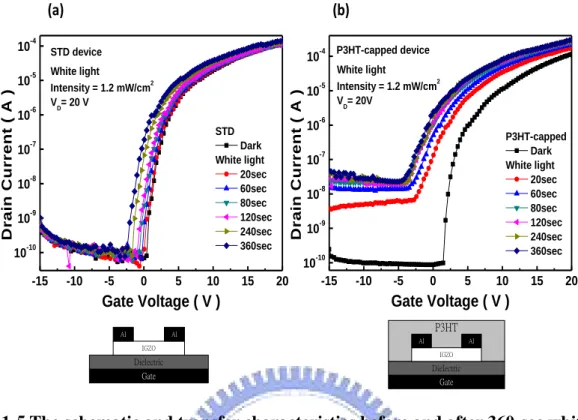
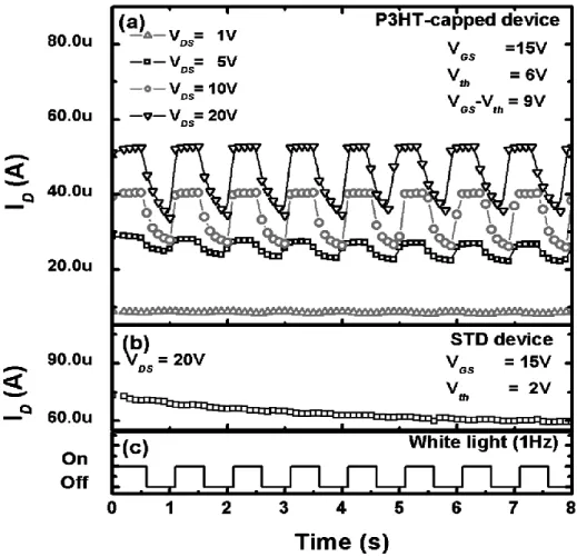
In previous report [29], an additional capping layer is used to improve the optical response of a-IGZO as shown in Fig. 1.5, and the additional light current with polymeric capping layer, forms P3HT/IGZO p-n junction,compared to standard device is due to the electrons accumulated from back channel in the band bending region near the drain side when the device is operated in saturation mode, as shown in Fig. 1.6. The accumulated electrons cause threshold voltage shift of a-IGZO TFT, which can be use to sense visible light. As shown in Fig. 1.7, on currents of P3HT-capped and standard devices monitored under pulsed illumination of 1 Hz frequency, which shows rapid and significant current response is
obtained in the saturation region (VDS=20 and 10 V). In the linear region, small response is
obtained when VDS=5 V and no response is observed when VDS=1 V. The different results are
attributed to band bending conditions of P3HT/IGZO p-n junction.
1-2
Motivation
In display technology, the threshold voltage should be precisely controlled to achieve stable current operation. Base on the result of a-IGZO visible light phototransistor [29], the threshold voltage is very sensitive to carrier concentration on the back channel of a-IGZO TFT, and can be effective influenced by capping layer’s work function. Therefore, we put series of metal with different work functions on the back channel of a-IGZO TFT to observe the variations of threshold voltage shift respect to different work function. If threshold voltage
7
of a-IGZO TFT can be controlled by capping layer with different work function, unnecessary to apply an addition voltage to like in duel gate structure, it is a simple and powerful method could be applied to display technology.
Furthermore, the capping layer might improve the sensitivity of a-IGZO TFT to detect bio/chemical molecules. In this study we capped a sensing layer, (poly(3-hexylthiophene) (P3HT) and copper phthalocyanine (CuPc)) , onto standard device and detect NH3 and acetone,
as vapor sensors. It is important for the development of non-invasive diagnostic breath analysis system [30-32]. For example, the breath NH3 concentration is higher in patients with liver
diseases or disturbed urea balance (~ 0.7 ppm) than that in normal person (< 0.3 ppm) [32]. Patients with diabetes exhale higher concentration of acetone than normal persons. Nitric oxide (NO) gas sensor is important for asthma attack prevention [32].
The of field effect mobility of a-IGZO TFT influenced by the capping layer is also an important topic to investigate. Capping different material and comparing the variation of mobility were demonstrated in this study. The result might give the way to improve mobility of metal oxide TFT by introducing a capping layer on the channel region, and could be applied to display technology.
8
1-3
FIGURES OF CHAPTER 1
Fig. 1-1 The carrier transport paths in covalent semiconductors [7].
9
Fig. 1-3 The overlap between the adjacent orbitals [2].
10
Fig. 1-5 The schematic and transfer characteristics before and after 360-sec white light illumination of (a) conventional a-IGZO TFT (STD device) (b) P3HT capped a-IGZO
TFT. [29]
Fig. 1-6 Schematic energy-band diagram of the P3HT-capped a-IGZO TFT near the drain side when device is operated in saturation mode.
-15 -10 -5 0 5 10 15 20 10-10 10-9 10-8 10-7 10-6 10-5 10-4 STD device White light Intensity = 1.2 mW/cm2 V D= 20 V STD Dark White light 20sec 60sec 80sec 120sec 240sec 360sec D r a in C u r r e n t ( A ) Gate Voltage ( V ) -15 -10 -5 0 5 10 15 20 10-10 10-9 10-8 10-7 10-6 10-5 10-4 P3HT-capped device White light Intensity = 1.2 mW/cm2 V D= 20V P3HT-capped Dark White light 20sec 60sec 80sec 120sec 240sec 360sec D r a in C u r r e n t ( A ) Gate Voltage ( V ) Gate Dielectric IGZO
Al Al Narrow Bandgap Absorption Layer
Gate Dielectric IGZO Al Al P3HT (a) (b)
11
Fig. 1-7 On currents of P3HT-capped and standard devices monitored under pulsed illumination of 1 Hz frequency.
12
Chapter 2 EXPERIMENTAL PROCEDURE
2-1
Device structure and fabrication
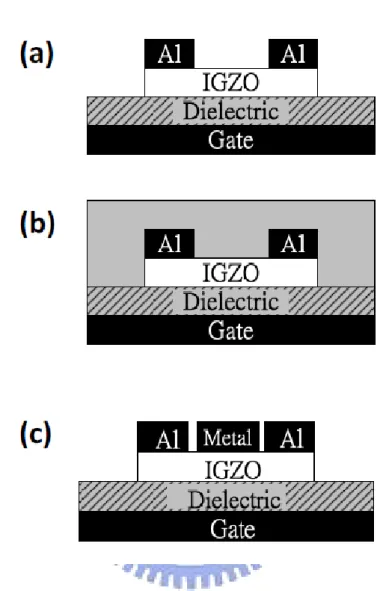
Heavily doped p-type Si (100) was used as a substrate and a gate electrode. Figure 2.1 (a) shows a schematic cross-section of the top-contact bottom-gate a-IGZO TFT structure (b) sensing-layer capped the top-contact bottom-gate a-IGZO TFT structure (c) metal-capped the top-contact bottom-gate a-IGZO TFT structure are used in this study. The detail fabrication process including dielectric deposition, a-IGZO film deposition, source/drain deposition, P3HT capping layer deposition and metal capping layer deposition are described in the following sections.
2-1.1 Dielectric deposition
The dielectric silicon nitride (SiNx) was formed on all samples with 1000 Å using Horizontal Furnace. Before deposition the active layer, the standard clean was carried out to remove the contamination on the dielectric surface. The standard clean is accomplished in two steps, SC1 and SC2. SC1 clean is the first step to remove the particle on the surface. The process was executed with a mixture of ammonium hydroxide, an oxidant hydrogen peroxide, and water in a mixing ratio of 1:4:20.
NH4OH:H2O2:H2O = 1:4:20 (SC1)
The SC2 clean was used to remove metals from the surface. The cleaning process inSC2 contain three solution of HCl, hydrogen peroxide, and water. The mixture ratio inthe SC2 process was 1:1:6.
13
2-1.2 a-IGZO film deposition
Generally, pulsed laser deposition (PLD) and ratio frequency (RF) –magnetron sputter were reported to deposit a-IGZO film as channel [33,34]. In this study, the rf-sputter with 3-in. circular target: In2O3:Ga2O3:ZnO = 1:1:1 at.% was used to deposit
the a-IGZO film. 35nm a-IGZO channel layer was deposited at room temperature with a power of 70W, a working pressure of 7mTorr, and an Ar/O2 flow rate of 30/0. The
active layer patterning was defined using a shadow mask.
RF sputtering (Fig. 2.2) is a process using radio frequency power supply, operating at 13.56MHz, to generate plasma in which atoms, ions, and clusters are created to sputter the target material. The glow-discharge between a target and a substrate, it’s consists of plasma with an equal number of working gas (Ar) and electrons. The ions are accelerated towards to the target by a strong electric field on the target due to the flux of electrons. Consequently, the ions hit the target to eject the target atoms, which are then re-deposited onto the substrate. RF sputtering is performed at low pressure, to increase the mean free path, the distance between collisions, and to improve the quality of the deposited film.
2-1.3 Source/Drain deposition
The metal in source/drain contacts was deposited using thermal evaporator. The base pressure of the thermal evaporator is 4×10⁻⁶ torr, and 50nm-thick Aluminum (Al)
is deposited through a shadow mask to form the source and drain contacts.
2-1.4 Post-annealing
14
annealing process at 350 oC in nitrogen (N2) furnace for 1hr, the base pressure is atmospheric
pressure, and the N2 flow rate is 10 liter per minute (L/min).
2-1.5 Sensing layers deposition
For P3HT-capped devices, P3HT (RR>98.5%, Rieke Metals Inc.) derived from chlorobenzene (1.5 wt%) was coated on some STD devices in 7000 rpm; the coated devices were then annealed at 200 °C for 10 min. The thickness of the P3HT film was 20 nm. For CuPC-capped devices, a 50-nm-thick CuPc (purity>99%, Lumtec) was deposited on the STD device by thermal evaporation at room temperature with a deposition rate as 0.5 Å/sec under 2×10⁻⁶ torr.
2-1.6 Metal capping layer deposition
The Body metal capping layer on the a-IGZO TFT back channel was deposited using thermal evaporator. The base pressure of the thermal evaporator is 4×10⁻⁶ torr and
the thickness of metal capping layer is 50nm.
2-2
Analysis instrument
2-2.1 Current-Voltage measurement instrument
In this study, all electrical characteristics were measured by semiconductor parameter analyzer (Agilent 4156) at room temperature in ambient air.
15
2-2.2 Micro-fluid gas sensing system
As shown in Fig. 2.3, various NH3 concentration is obtained by uniformly mixing
various amount of NH3 (from a cylinder contains 100 ppm NH3) with high purity
nitrogen (N2) into a 20-cm-long U-shape tube. The amount of N2 is controlled by a
mass-flow controller. The amount of 100 ppm NH3 is controlled by an electrical
syringe pump. The U-shape tube with mixed gas is connected to a micro-fluid measuring system made by Polytetrafluoroethylene (PTFE) (width = 1 cm, length = 3.5 cm, and height = 0.1 cm). Two Keithley 2400s are utilized to synchronously generate 20 V (drain terminal) and 5V (gate terminal) pulse each 50 millisecond and read out the currents.
2-3
Methods of device parameters extraction
In this section, the extractions of the device parameters are discussed in details. The field effect mobility, threshold voltage (VTH), turn on voltage (Von), the on/off
current ratio (Ion/Ioff), the sub-threshold swing (S.S) are extracted and assessed,
respectively.
2-3.1 Mobility
Mobility is a measurement of the velocity of the carrier move through a
Material[35]. A higher mobility allows for higher frequency response such as the time it takes for the device to transfer from off state to on state. In the off state, few current flows through the device. In the on state, large amount of currents flow through the device. A large mobility means the device can conduct more current. The mobility in this study was extracted from the saturation region. The device was operated at
16
drain-voltage of 20V, since the threshold voltage was much lower than 20V. The saturation mobility is determined from the transconductance, define by
[ ] D D V const G I gm V (2.1)
The drift component of drain current is
2 1 ( ) 2 D OX GS TH W I C V V L (2.2)
When the mobility is determined, the transconductance is usually taken to be
2 ox W C gm L (2.3)
When this expression is solved for the mobility, it is known as the saturation mobility 2 2 [ m ] sat Saturation OX g W C L (2.4)
2-3.2 Turn-on voltage (Von)
Turn-on voltage (Von) is identified as the gate voltage at which the drain current
begins to increase in a transfer curve. Von can directly characterizes the gate voltage
required to fully“turn off"the transistor in a switching application.
2-3.3 Threshold voltage (Vth)
Threshold voltage is related to the operation voltage and power consumptions of TFTs. We extract the threshold voltage from equation (2.5), the intercept point of the square-root of drain current versus voltage when devices operate in saturation mode
( ) 2 D OX G TH W I C V V L (2.5)
17
2-3.4 Ion/Ioff current ratio
The Ion/Ioff (on/off) ratio represents large turn-on current and small off current. It
is an indicator of how well a device will work as a switch. A large on/off current ration means there are enough turn-on current to drive the pixel and low off current to maintain in low consumption.
2-3.5 Sub-threshold swing (S.S)
Another important characteristic for device application is sub-threshold swing. It is a measurement of how rapidly the device switches from off state to on state. Moreover, the sub-threshold swing also represents the interface quality and the defect density [40].
(log ) [ ] D D V const G I S V (2-1)
If we want to have a better performance TFTs, we need to lower the sub-threshold swing.
18
2-4
FIGURE OF CHAPTER 2
Fig. 2-1 The schematic cross-section of the (a) conventional top-contact bottom-gate a-IGZO TFT. (b) Sensing layer capped the top-contact bottom-gate
19
Fig. 2-2 RF-power sputtering deposition system.
20
Chapter 3 RESULTS AND DISSCUSION
3-1
Dual gate indium-gallium-zinc-oxide thin film transistor with an
unisolated floating metal gate for threshold voltage modulation
and mobility enhancement
In this study, we proposed a modified double gate a-IGZO TFT that can adjust the threshold voltage in both positive and negative directions without the additional dielectric layer and power supply. The control gate metal is formed directly on the back interface of the IGZO active layer. There is no dielectric layer between the IGZO body and the control gate, indicating a metal-semiconductor (MS) back gate. During device operation, the back gate is floated, and therefore the power supply for the back gate is not necessary. The back gate bias (VBG) is
provided from the intrinsic built-in voltage across the IGZO body and the back gate. Because there is no dielectric layer beside the back gate, the control ability of the floating back gate is better than that of the conventional back gate formed by a metal-oxide semiconductor (MOS) diode. By choosing a floating back gate that processes work function higher or lower than that of IGZO (ψIGZO), we can significantly move the threshold voltage(from - 5.0 to 7.9 V).
3-1.1 Motivation
According to the experiment results mentioned before [29], threshold voltage influenced by light induced carriers at the back channel and about -7 volts shift was observed in transfer characteristic, as shown in Fig 3.1. That means threshold voltage is very sensitive to carrier concentration at the back channel. If capping materials with different work functions at the back channel, electrons can transfer inside or outside from the back interface due to the band
21
bending of a-IGZO to the capping material, threshold voltage could be modulated.
3-1.2 The threshold voltage varies with capping metallic layers with
different work functions
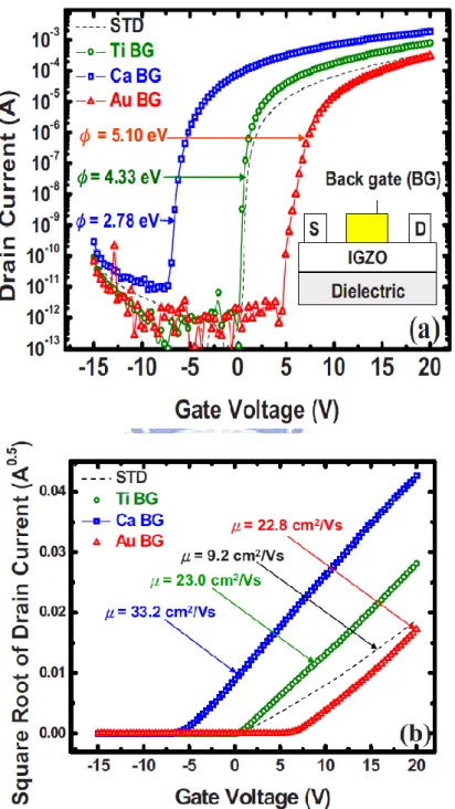
The channel width and length are 1000 um and 300 um, respectively. Then, the 150-um-long metallic back gate was deposited on the IGZO top surface of some standard (STD) devices to form the double gate devices as shown in the inset of Fig. 3.3(a). The capping layer is located between the source and drain contacts. Various metal materials with different work functions include calcium (Ca, φ Ca=2.78 eV), titanium (Ti, φ Ti=4.33 eV), copper (Cu,
φ Cu=4.65 eV), and gold (Au, φ Au=5.10 eV) were used as the floating back gate. Except Ca,
the thickness of these capped layers is fixed as 60 nm. For Ca, to avoid oxidation, 100-nm-thick Al is passivated onto the 35-nm-thick Ca. The threshold voltage and mobility are extracted from the slope and the x-axis intercept of the √ID-VGS curve measured under saturation
condition (VDS=20 V, VGS is scanned from -15 to 20 V). Fig. 3.3(a) presents the transfer
characteristics of the uncapped (STD), Ti-capped, Ca-capped, and Au-capped a-IGZO TFTs. As compared with the STD device, there are significant Vth shifts of -7.4 V and 5.5 V of the Ca-capped and Au-capped devices, respectively; a small Vth shift of -1.7 V of Ti-capped device is probed. Capping a metal layer (a control gate without insulator) on the IGZO back surface does not form a current leakage path to increase SS and leakage current. In Fig.3.3 (b), the slopes of √ID-VG curves are raised by metallic capping layers, indicating a significantly
improved field effective mobility. Table. 3-1 lists the extracted typical parameters of a-IGZO TFTs with various metallic capping layers. A tunable Vth ranges from -5.0 to 7.9 V is demonstrated. Where the threshold voltage shift (ΔVth) is the threshold voltage difference between STD device and the floating dual gate (FDG) device. Besides, all these FDG devices
22
possess an improved field-effect mobility, a comparable SS (0.16–0.33 V/dec) and a high on/off current ratio (>2.6×10⁸).
3-1.3 Mechanism of threshold voltage shift from metal capping.
The back gate bias (VBG) is contributed from the intrinsic built-in voltage between IGZO
body and the floating back gate. As shown in Figs. 3.4(a) and (b), before contact, the Fermi-level in Au and Ca are lower and higher than that of IGZO, respectively. After IGZO contacts with Au, the thermal equilibrium is attained with a constant Fermi-level. The electrons in IGZO flow into Au to form a built-in voltage and a depleted IGZO body as shown in Fig. 3.4(c). The system can be regarded as a conventional dual gate TFT that has a control gate with a negative gate-to-source voltage (always off).The voltage is contributed from the work function difference,(ψIGZO−ψAu) e, where e is the electron charge. Because Au depletes the IGZO body, the channel formation on the dielectric will be suppressed and the Vth is increased (enhancement mode TFT). On the contrary, as shown in Fig. 2.4(d), Ca injects electrons into IGZO body. The injected electrons accumulate near the interface between IGZO and Ca to form a channel. The system can be regarded as a conventional dual gate TFT that has a control gate with a positive gate-tosource voltage _always on_. The voltage is contributed from the work function difference, (ψIGZO−ψCa)e. Because Ca generates a channel on the IGZO back surface, the Vth becomes more negative to suppress the initially existed channel
to turn-off the device (depletion mode TFT). Due to the thin active layer (e.g., 35 nm), the devices are operated with a fully-depleted IGZO body.[36],[37] The proposed double gate transistor can be regarded as a composition of three capacitors. They are the capacitor of the bottom main gate (CG, which is formed by the gate dielectric), the depletion capacitor (CD,
23
formed by the MS back gate contact).[37] In the case of the enhancement mode operation, the channel forms on the dielectric surface and the body is depleted by the back gate. Therefore, the channel is located between CG and CD as shown in the bottom of Fig. 3.4(c). On the contrary, in
the case of the depletion mode operation, the channel forms on the interface between IGZO and the back gate and the IGZO body is depleted by the bottom gate. Therefore, the channel is located between CD and CBG as shown in the bottom of Fig. 3.4(d). Under enhancement mode
operations, the back-gate-voltage dependent threshold voltage shift (dVth) can be estimated by the formulas as: dVthCG=−dVBG[CDCBGCD+CBG]. Under depletion mode operation, dVth can
be given as dVth[CGCDCG+CD]= −dVBGCBG.[37] Compared to the conventional dual gate TFT
that uses a MOS diode as the back gate, the MS back gate contact in this study leads to a high capacitor (CBG). As a result, a small back gate voltage (VBG) can shift the Vth significantly. The
derivation of Vth to back gate voltage, dVth dVBG, is as high as 5 for the proposed dual gate
TFT.
3-1.4 Influence of a-IGZO thickness in dual gate structure
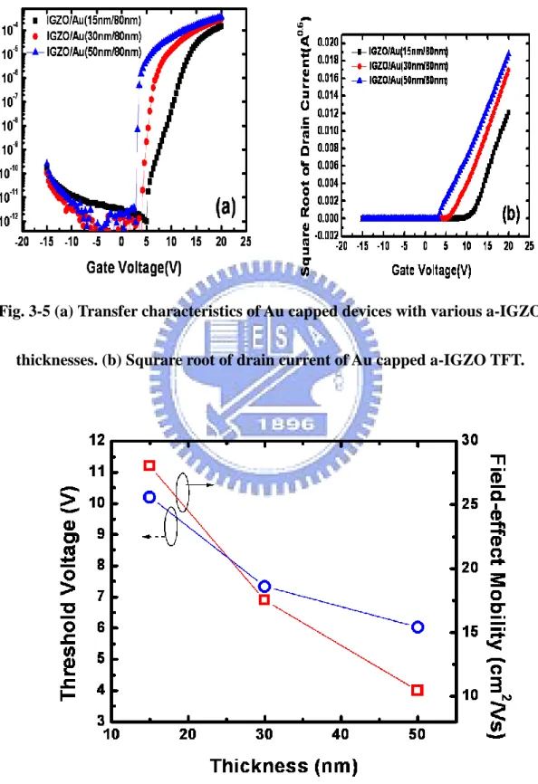
For the dual gate structure, the thickness of a-IGZO influences the control ability of main gate. In Fig 3.5(a), three standard devices with various a-IGZO thicknesses(15nm, 30nm, 50nm) capped with 80nm of Au, threshold voltage and mobility have strong dependence with a-IGZO thickness. As show in Fig 3.5(b), threshold voltage become more positive as a-IGZO thickness decrease indicates back gate becomes more dominant, and its cost higher voltage for main gate to turn on the device as shown in Fig 3.6 and parameters are listed in Table 3.2. On the contrary, as the a-IGZO thickness increase, it has barely threshold voltage shift after Au capped. Mobility is also affected by the thickness of a-IGZO film, as thickness of a-IGZO decrease, higher mobility is measured. This trend might be explained as the reduction of scattering effect
24
in dual gate structure or a parasite back channel will be discussed in the next section.
3-1.5 Mobility enhancement and equivalent circuit of dual gate
structure
In this study, 2 to 3 times increment of mobility has been observed, and the voltage between floating gate and source has been measured as shown in Fig. 3.7. As VGS larger then
VTH, floating gate start to couple the voltage of main gate and induces the second channel under
it. The equivalent circuit is shown in Fig. 3.8, and the voltage of floating gate, VDS×(R2/R1+R2),is influenced by its position. The limitation of mobility is due to two gaps of
uncapped region. If the capping ratio increases, higher mobility value can be obtained.
3-1.6 An inverter comprised of an enhancement-mode and a
depletion-mode a-IGZO TFT
An inverter comprised of an enhancement-mode a-IGZO TFT (Ti back gate) to serve as a switch and a depletion-mode a-IGZO TFT (Ca back gate) to serve as the load is demonstrated as shown in the inset of Fig. 3.9. The voltage transfer curve and the voltage gain of the inverter is shown in Fig. 3.9. With a supply voltage (VDD) of 20 V, a signal inversion behavior with a
maximum voltage gain of -39 V/V is obtained. The maximum input voltage that will be recognized as a low input logic level (VIL) is 1.6 V. The minimum input voltage that will be
recognized as a high input logic level (VIH) is 2.7 V. The output high voltage (VOH) is 20 V and
the output low voltage (VOL) is 0.4 V. The transfer width, defined as VIH−VIL, is only 1.2 V. In
this study, a dual gate IGZO TFT with a floating MS back contact is proposed to modulate the threshold voltage and to increase the field-effect mobility. The floating back gate has a
25
back-gate bias (VBG) contributed from the built-in voltage between the IGZO and the capping
metal. By using various floating metals, a depletion mode or an enhancement mode dual gate TFT can be achieved. An improved mobility is also obtained in the proposed FDG TFT. An inverter comprised of the proposed dual gate a-IGZO TFTs has a maximum voltage gain of -39 V/V with a supply voltage of 20 V.
3-2 A novel approach to improve biochemical sensitivity
of indium-gallium-zinc-oxide thin film transistor
(IGZO TFT) by capping sensing layer on active layer
Metal oxide semiconductor has many benefits beyond organic semiconductor for it stable in operation, low temperature fabrication, simple structure, less insensitive to oxygen and moisture than OTFTs, and can sensing in liquid surrounding. Base on those characteristics, metal oxide semiconductor is a possible candidate for next generation of biochemical sensor. However, metal oxide semiconductor is less sensitive to biochemical particles than organic material, so a sensing layer can be added to solve this problem and sensitivity can be also improved. By alternating the sensing layer, different biochemical particles can be detected.3-2.1 Electrical properties of IGZO capping different material
For detect certain gases, we chose P3HT( 3 - H e x y l t h i o p h e n e ) to detect ammonia and nitride oxide, and CuPC( C o p p e r p h t h a l o c ya n i n e ) to detect acetone.
To make sure that the capping materials does not cause the damage of electrical properties of a-IGZO film by measure transfer and output characteristics. Thickness influence of sensing material is also considered, and electrical characteristics of a-IGZO capped with different
26
thickness of P3HT and CuPC is measured. It shows that IGZO TFT keeps its field-effect control, and no obvious decrement of mobility has been observed. For P3HT capped device, threshold voltage varies with P3HT thickness , shown in Fig. 3.10 , can be attribute to the heating process to solidify P3HT solution in glove box. Glove box is full of N2, therefore
oxygen is tend to escape from the surface from IGZO film under heating process, and it is reasonable that thicker P3HT capped a-IGZO TFT has lesser threshold voltage shift. For CuPC capping, deposited under thermal evaporation, does not exhibit large threshold voltage shift and mobility variation after capping as shown in Fig. 3.11. All parameters are shown in Table 3.3.
3-2.2 Ammonia sensing properties of P3HT capped IGZO TFT
The responses of standard (STD) a-IGZO TFT and P3HT-capped a-IGZO TFT to ammonia are investigated. Drain current variations (I) of these two devices are plotted as a function of time exposed to different ammonia concentration in Fig.3.12. Devices are biased at VGS-VTH=5V and VDS=20 V. For STD device, no significant response can be observed when
ammonia concentration is 10 ppm. For P3HT-capped device, an obvious current drop is obtained when device is exposed to ammonia. After the removal of ammonia, the current drop is recovered. The ammonia sensing response of a P3HT-based OTFT has been reported with ammonia concentration ranging from 10 to 100 ppm. [38] In that report, ammonia molecules behave as acceptor-like deep trap states (or as electron donors) to trap the holes at the P3HT/dielectric interface, shift the threshold voltage to be more negative and cause a current drop. In our study, a positive threshold voltage shift is observed when device is exposed to ammonia as shown in the Fig. 3.14. In our work, a clear response to 0.2 ppm ammonia is observed as shown in Fig 3.15. The sensing sensitivity is also strongly influenced by the
27
thickness of P3HT. When the thickness of P3HT increases to be 70 nm, the response to 10-ppm ammonia becomes almost invisible as shown in the in Fig 3.13.
3-2.3 Nitride oxide sensing properties of P3HTand PbPC capped IGZO
TFT
A typical oxidizing gas, nitric oxide (NO), is used to stimulate the P3HT-capped device. Drain current variations (I) of STD device and of P3HT-capped device are plotted as a function of time exposed to different NO concentration in Fig.3.16. Devices are biased at VGS-VTH=8.6 V and VDS=20 V. When standard device is exposed to NO gas, a slow current
drop is observed. The current drop is not able to be recovered even when NO is removed. The slow and irreversible response is due to the slow adsorption and desorption of NO molecules on the oxide semiconductor thin film. [32]. When P3HT-capped a-IGZO TFT is exposed to NO, on the contrary, a fast current increase is observed. A fast recovery behavior is also obtained when NO is removed. The P3HT capping successfully blocks the reaction between NO and
a-IGZO film. The sensing behavior is dominated by the reaction between NO and P3HT in
which NO molecules act as oxidizing agents to withdraw electrons from P3HT.[39] The positive potential on P3HT film helps to turn on the transistor and thus increase the current of
a-IGZO TFT.
3-2.4 Acetone sensing properties of CuPC capped IGZO TFT
Copper phthalocyanine (CuPc) is capped onto the back channel of a-IGZO TFT to detect a kind of reducing gas, acetone, which is an index gas in the breath of patients with metabolic disease like diabetes mellitus.[31] Drain current variations (I) of standard device and CuPC-capped device are plotted as a function of time exposed to different acetone
28
concentration in Fig. 3.17. Devices are biased at VGS-VTH=0.5 V and VDS=1 V. For standard
device, no clear response to acetone can be observed, indicating a weak charge transfer interaction between the a-IGZO and acetone at room temperature. For CuPC capped a-IGZO TFT, on the contrary, a fast, sensitive, and reversible response to acetone is obtained. The response current variation ratio (IDS/I0 when sensing time is fixed as 120 sec) is plotted as a
function of acetone concentration in Fig. 3.18 A linear relationship is observed. The sensing sensitivity is as high as 100 ppb and is promising to be used to distinguish healthy humans ( 900 ppb) and diabetes patients ( 1800 ppb).
3-2.5 Sensing mechanism of hybrid IGZO gas sensors
The organic layer and the a-IGZO film form a p-n junction. Oxidizing or reducing vapor molecules act like electron acceptors or electron donors to change the potential of the organic sensing layer and thus change the energy band equilibrium of the p-n junction. As a result, the current of a-IGZO TFT is significantly changed. The proposed mechanism has been utilized to form a sensitive visible light sensor in previous report. [29] In that work, visible light absorbed by the organic capping layer produces electron-hole pair, injects electrons into a-IGZO film, and changes the TFT threshold voltage. In another work, we capped various kinds of metals onto the back interface of a-IGZO TFT. The built-in potential between the floating capping metal and a-IGZO is utilized to adjust the device threshold voltage. The capping layer is served as a floating second gate to influence the characteristics of a-IGZO TFT as shown in the Fig. 3.19. When the organic sensing layer (OSL) is exposed to oxidizing or reducing gases, the potential of the OSL is changed. Since the OSL is treated as a floating second gate, the potential variation of the OSL significantly influences the current of the a-IGZO TFT.
29
P3HT. The negative potential on P3HT layer, the second gate, shifts the threshold voltage to be more positive and produces a current drop in a-IGZO TFT. The sensing sensitivity is high because the threshold voltage is sensitive to the body potential.
3-2.6 The relationship between sensitivity and gate bias
An interesting gate-bias-dependent sensing sensitivity is also found when changing the bias conditions during sensing. As shown in Fig. 3.20, the current variation ratio (IDS/I0) is
plotted as a function of time when devices are exposed to 5-ppm acetone and recovered in pure nitrogen under different bias condition. When VGS-VTH=5 V and VDS=1 V, IDS/I0 is less
than 0.04 and is similar to IDS/I0 of the floating gate condition, implying that the sensing
mechanism is similar to a chemical resistor rather than a chemical transistor. When VGS-VTH=0.5 V and VDS=1 V, IDS/I0 is improved 5.5 times and reaches 0.22. The
gate-bias-dependent sensitivity can be explained as follows. When VGS is large, the channel
carriers are mostly induced and controlled by VGS. The potential variation of the OSL (i.e. the
second gate) caused by the charge transfer between acetone and the OSL is much smaller than VGS. Thus, the channel current has only a weak response to the acetone molecules. When
VGS-VTH=0.5 V, the potential variation of the OSL is comparable to VGS-VTH. The channel
current is then significantly influenced by the charge transfer between the OSL and gas molecules.
30
3-3
High mobility a-IGZO TFT with Ca/Al capping layer
In the previous experiment, we capped different metals on the back side of a-IGZO TFT, shown in Fig. 3.3, and an interesting result has been found. The mobility of Ca/Al capped devices is always higher than others, and more the 10 times mobility enhancement can be reached by Ca/Al capping.
In this section, a set of experiments have been demonstrated to investigate the high mobility effect (about than 10 times increment) found in Ca/Al capped a-IGZO TFT. The comparison of Ti capped and high mobility Ca/Al capped devices are shown in Fig.3.21, and listed in Table 3.4.
3-3.1 Transfer characteristics and time decay of Ca/Al capped TFT
After Ca/Al capping, we trace the device for 50 days, as shown in Fig 3.22. Variation of threshold voltage and mobility during 50 days is shown in Fig 3.23. As Ca/Al capped, threshold voltage became negative. To explain the threshold voltage shift, the work function of Ca is 2.8 eV, much higher than the Fermi level of a- IGZO (~ 4.5 eV). And the shift of threshold voltage can be explained by the electrons injection from calcium into a-IGZO due to the work function difference as a back gate discussed in section 3-1. A negative gate bias is needed to deplete the active layer and to turn off the device. When devices are exposed to air, the rapid oxidation of Ca eliminates the threshold voltage shift. An explanation includes two mechanisms is proposed for mobility surge compare to cap with other metals (eg. Al, Ti, Au) demonstrated in section 3-1. The first mechanism is that, for metal oxide semiconductors, oxygen vacancies can be regarded as doping forms highly conductive regions cause high mobility, and variation of oxygen concentration in a-IGZO film due increment of oxygen vacancies at the edge and under Ca capping layer due to the formation of Ca-O bonds.
31
Gradually decrement of mobility after exposed to air can be explained as the reduction of oxygen vacancies in oxygen rich surrounding.
The second mechanism is defect reduction in a-IGZO film after eliminated weak-bonded oxygen by oxidation of Ca, by forming Ca-O, and that may reduce the shallow traps in metal oxide semiconductor and lower energy barriers which limit electrons transport. After 30 days, the device has threshold voltage around -0.5 and mobility about 90cm2/VS, the device
becomes stable and keeps high mobility. Detail parameters are listed in Table 3.5.
3-3.2 .Stability test of Ca/Al capped IGZO TFT
Stability is also an important issue to know if Ca/Al capping causes degradation of a-IGZO film, which limits this work in practical application. A positive bias stress (PBS) and negative bias stress (NBS) is demonstrated. (VG-VT=20 for PBS and VG-VT=-20 for NBS, and
VD was not supplied during bias stress.) The transfer characteristics and threshold voltage shift
as shown in Fig. 3.24. After same bias time, similar voltage shift for Ca/Al capped and standard device indicates Ca/Al capping doesn’t degrade the stability.
3-3.3 .a-IGZO thickness effect of Ca/Al capped TFT
The a-IGZO thickness effect of Ca/ Al capped device is investigated, and the mobility enhancement effect become inferior when IGZO thicknesses increases as shown in Fig. 3.25 Table3.6 lists the extracted parameters for standard (in parentheses) and Ca/Al capped devices with various a-IGZO thicknesses. As discussed before, we supposed the mobility surge after Ca/Al capped attribute to the reduction of shallow traps in a-IGZO film at the interface of Ca/a-IGZO. The defect reduction effect is very sensitive to the distance of Ca/a-IGZO interface and the front channel of bottom gate a-IGZO TFT, and this result supports defect reduction
32
postulation for the trap-reduction effect is suppressed when the front channel is far from the Ca/a-IGZO interface.
3-3.4 Measurement in glove box
Glove box maintains experimental surrounding under low oxygen (<0.1ppm) and low moisture (<0.1ppm) condition, which provides a stable environment to observe variations of device electrical characteristics caused by oxidation of Ca. The capping procedure and electrical measurement has been conducted in glove box. To prevent gate leakage current due to the large pad for measuring in glove box, thicker insulator (200nm) is used. The length and width are 600um and 1000um respectively, and the capping ratio is kept the same (capping length is 300um).
Firstly, comparison of measure standard device inside and outside glove box is demonstrated, and a little threshold voltage shift and mobility increment were observed as shown in Fig.3.26. The variation of transfer characteristic can be explained as the variation of oxygen concentration and carrier concentration of a-IGZO back interface. After Ca/ Al capping, observation in several days are shown in Fig. 3.27 and Table 3.7. The mobility increase 10 times and the threshold voltage recover become much slower compared to observe in air can be explained as slower oxidation rate of Ca keeping the carrier injection by work function difference and, however, mobility is still gradually decrease. In this experiment, we found the threshold voltage shift (caused by electrons injection) is unlikely to have strong relationship to mobility surge effect, therefore, the main we suppose the mobility surge is mainly caused by the defect reduction effect.
33
3-3.5 Unannealed a-IGZO device capped with Ca/Al
The unanneled a-IGZO film has larger subgap DOS and shallow traps than annealed one. Ca/Al is capped on a-IGZO without thermal annealing to investigate if Ca/Al capping can reduce the shallow defects by reducing weak-bonded oxygen in a-IGZO film and improve electrical conductivity and stability. As shown in Fig3.28 (a) a-IGZO film without thermal annealing with high electrical resistance shows no field effect turn on. After Ca capping, the conductivity of IGZO film has much improved, which can be explained as large amount of weak-bonded oxygen were removed from a-IGZO film by formation of Ca-O bonds. Then the device has been placed for several days (8 days) and measured again, it showed well transfer characteristic and output characteristic, Fig 3.28(b), result from reduction of shallow traps in a-IGZO film.
We also checked the stability by measured 7times in sequence, and compared the result with uncapped one, as shown in Fig 3.28 (c) and (d). The Ca/Al capped device is more stable the uncapped one, which indicates bulk defects is suppressed by capping.
3-3.6 Similar behaviors of Si oxide capped to Ca/Al capped IGZO TFT
To understand relation between mobility increment and the oxidation of capping layer, several materials is capped on a-IGZO film and compared the mobility variations, as shown in Fig 3.29 and Table 3.8. For oxide with the highest oxidation state (can’t be oxidized anymore), the mobilities does not increase significantly after capping, even decrease for HfO2. However,
SiO greatly enhance the mobility, which mainly is best considered as an inhomogenous mixture composes of Si and SiO2 [47, 48] at the interface of SiO/a-IGZO. Si might lower
oxygen concentration by forming oxide as the interface of SiO/IGZO in a-IGZO like Ca. And the result indicates oxidization tendency of capping layer has strong relationship with the
34
mobility surge. Materials can reach higher oxidized valance number and are possible candidate to cause mobility surge.
Then we investigate the mobility decay after capping of SiO, as shown in Fig. 3.30 and Table 3.9. It shows that the mobility decrease much faster than Ca/Al capped device, and we guess the faster decrease rate is due to rapid decrement of oxygen vacancies.
3-3.7 Activation energy extracted from Ca/Al capped device
To verify the trap-reduction mechanism is to compare the activation energy of the standard and the Ca/Al-capped devices. Thermal stress has been conducted to extract the activation energy. The transfer characteristics of standard and of Ca/Al capped devices under different temperature are shown at Fig.3.31 (a) and (b), respectively The Arrhenius plots fitted by the following equation: 0
Ea kT D D
I I e
for the standard device and of Ca/Al-capped device are shown in Fig. 3.31(c) and(d), respectively. The extracted activation energy of these two devices are compared in Fig. 3.32. The x-axis represents the gate bias minus the initial (room-temperature) threshold voltage. Apparently, devices with Ca/Al capping layer exhibit lower activation energy than the standard ones, suggesting that the energy barrier for electron transport is lower in Ca/Al-capped devices.
3-3.8 XPS analysis of Ca/Al capped device
Finally, XPS analysis is used to exam the variation of oxygen concentration caused by Ca/Al capping. We supposed that the oxygen concentration of a-IGZO film is lower near the edge and under the Ca/Al capping layer for the formation of Ca-O bonds. A clean glass substrate is prepared with 30nm a-IGZO film above, and half of it was capped with 20nm Ca layer. We analysis two points, one is near the Ca capping layer and one is far from it as show in Fig. 3.33(a) The C 1s at 284.6eV was used as the reference to calibrate the energy positions of all
![Fig. 1-1 The carrier transport paths in covalent semiconductors [7].](https://thumb-ap.123doks.com/thumbv2/9libinfo/8756085.206935/23.892.215.711.131.919/fig-carrier-transport-paths-covalent-semiconductors.webp)
![Fig. 1-4 Schematic cross section of dual-gate a-IGZO TFT [28]](https://thumb-ap.123doks.com/thumbv2/9libinfo/8756085.206935/24.892.295.655.483.778/fig-schematic-cross-section-dual-gate-igzo-tft.webp)
![Fig. 3-1 The threshold voltage shift as a function of illumination time of standard device and P3HT capped a-IGZO TFT.[29]](https://thumb-ap.123doks.com/thumbv2/9libinfo/8756085.206935/51.892.143.803.189.939/threshold-voltage-shift-function-illumination-standard-device-capped.webp)