國
立
交
通
大
學
電子工程學系 電子研究所碩士班
碩
士
論
文
適應性電壓調變應用於離散餘弦轉換
Adaptive Voltage Scaling
for Discrete Cosine Transform
研 究 生:劉仲文
指導教授:黃 威 教授
中 華 民 國 九 十 八 年 七 月
適應性電壓調變應用於離散餘弦轉換
Adaptive Voltage Scaling
for Discrete Cosine Transform
研 究 生:劉仲文 Student:Chun-Wen Liu
指導教授:黃 威 教授 Advisor:Prof. Wei Hwang
國 立 交 通 大 學 電 子 工 程 學 系 電 子 研 究 所 碩 士 論 文
A Thesis
Submitted to Department of Electronics Engineering & Institute of Electronics College of Electrical Engineering and Computer Science
National Chiao Tung University in Partial Fulfillment of the Requirements
for the Degree of Master in Electronics Engineering
July 2008
Hsinchu, Taiwan, Republic of China
適應性電壓調變應用於離散餘弦轉換
學生:劉仲文 指導教授:黃 威 教授
國立交通大學電子工程學系電子研究所碩士班
摘要
適應性電壓調變是最有效用的技術在現今低功率積體電路設計
上。論文中提出一個新的可變電壓產生器。這個電壓產生器可以產生
在 0.8V 到 1.2V 之間的五種電壓。我們發展一個適合此可變電壓產生
器的適應性電壓控制器,將這兩者組合成為一個適應性電壓調變系
統。晶片上的可變電壓產生器在這個系統當中扮演很重要的角色,它
取代了在電壓調整時常用的晶片外的直流/直流轉換器。
離散餘弦定理已經成為數位訊號處理中被廣泛應用的轉換技巧之
一。我們將適應性電壓調變的系統應用在離散餘弦定理的處理器上然
後成功的減少了離散餘弦定理處理器最多 45%的電源消耗。所有的模
擬結果都是利用 TSMS 0.13 μm CMOS 的製程下得到。
Adaptive Voltage Scaling
for Discrete Cosine Transform
Student: Chun-Wen Liu Advisor: Prof. Wei-Hwang
Department of Electronics Engineering & Institute of Electronics
National Chiao-Tung University
ABSTRACT
In the modern digital IC system, adaptive voltage scaling is the most
efficient technology for low power design. A new variable voltage
generator (VVG) has been proposed in this paper. Five voltage levels
ranged from 0.8V to 1.2V can be generated. An adaptive voltage scaling
controller has been developed to fit the VVG to form an adaptive voltage
scaling control system. In stead of the off-chip DC-DC converter which is
often used in voltage regulation, the on-chip VVG takes an important roll
in this system.
Discrete Cosine Transform (DCT) has become one of the widely used
transform techniques in digital signal processing. The adaptive voltage
scaling system has been applied to DCT and reduces at most 45% power
consumption of DCT. All simulations are implemented in TSMC0.13-μm
CMOS technology.
Acknowledgements
I would like to express my deepest gratitude to my advisor Prof. Wei Hwang for his enthusiastic guidance and encouragement throughout the research. With his support, I have the confidence and energy to stride forward.
Following, I would like to thank all my friends, Po-Tsang Huang and Wei-Chih Hsieh at LPSOC lab. They gave me much support and discussion on my thesis research.
Finally, I give the greatest respect and love to my family, and I want to express my highest appreciation for their support and understanding.
Contents
1 Introduction1.1 Motivation of the Thesis………..1
1.2 Research Goal and Contributions………..1
1.3 Thesis Organization………...2
2 Voltage Scaling Techniques for Low Power 2.1 Introduction………..………4
2.2 Voltage Influence on Power………....4
2.3 Voltage Scaling Influence in Delay………...5
2.4 Voltage Scaling Techniques………...6
2.4.1 Multiple Supply Voltage………...6
2.4.2 Clustered Voltage Scaling (CVS)………...7
2.4.3 Multiple Threshold Voltage………...8
2.4.4 Adaptive Voltage Scaling (AVS)………....10
2.4.5 Adaptive Body Bias (ABB)………....11
2.5 Dynamic Voltage Scaling………..12
2.5.1 Essential Components………....12
2.5.2 Improving Energy Efficiency………....13
2.5.3 Fundamental Trade off………..14
2.6 Conversion Efficiency………...14
2.6.1 Limits to Reducing Cdd……….15
2.7 Design Constraints Over Voltage……….17
2.7.1 Circuit Design Constraints………17
2.7.2 Circuit Delay Variation………..18
2.7.3 Noise Margin Variation………..19
2.7.4 Delay Sensitivity………..22
3 Adaptive Voltage Scaling 3.1 Components of Adaptive Voltage Regulation………..24
3.2 Voltage Converter………..25
3.2.1 Pulsed Width Modulation (PWM) Operation………..26
3.2.2 Buck Converter………...27
3.2.3 Boost Converter………..28
3.2.4 Buck-Boost Converter………29
3.3 Reference Voltage Generator 3.3.1 Traditional Reference Voltage Generator……….30
3.3.2 Modified Variable Voltage Generator………...31
3.4.1 Output Buffer……….34
3.5 Simulation Result………..35
3.6 PLL-based Adaptive Voltage Regulation Using FSM………37
3.6.1 Reference circuit……….38
3.6.2 Finite State Machine (FSM)………...39
4 Discrete Cosine Transform 4.1 Introduction to Discrete Cosine Transform……….42
4.2 Alternative Implementation………..44
4.2.1 Multiplier Implementation………45
4.2.2 Pure ROM Implementation………...46
4.2.3 Mixed ROM Implementation………47
4.3 Reducing Power of DCT………...47
4.3.1 Reducing Power Through Pipelining………...47
4.3.2 Reducing Power Through Parallelism……….49
4.3.3 Reducing Power Through Reducing Complexity………...50
4.4 Reconfigurable Architecture………52
4.4.1 Computational Sharing Multiplier Algorithm (CSHM)…………53
4.4.2 DCT Coefficients for 4-bit Decomposition………..55
4.4.3 DCT Coefficients for 2-bit Decomposition………..56
4.4.4 DCT Architecture Based on CSHM Algorithm………..58
4.4.5 Modified DCT Coefficients………...61
4.5 Simulation Result………..62
5 Adaptive Voltage Scaling for Discrete Cosine Transform 5.1 The Proposed Architecture………...64
5.2 Reference Circuit………...65 5.2.1 Ring Oscillator………66 5.2.2 Frequency Detector………67 5.3 Controller………...69 5.3.1 Control Logic………..70 5.3.2 Selector………73 5.4 Simulation Result………..77
5.4.1 Adaptive Voltage Scaling System………..77
5.4.2 AVS for Discrete Cosine Transform………..79
List of Figures
22.1 Multiple Supply Voltage………..6
2.2 Level Converter………7
2.3 Clustered Voltage Scaling………7
2.4 Conventional Level Converting Flip-Flop………...8
2.5 Vdd vs. Vt for a Fixed Delay………...9
2.6 Multiple Threshold Voltage……….9
2.7 Frequency vs. Power of AVS and ABB……….10
2.8 Scheme of the Conventional AVS System………11
2.9 Adaptive Body Biasing………..12
2.10 Energy Efficiency Improvement………..13
2.11 Energy Loss Due to Voltage Supply Ripple………16
2.12 Relative CMOS Circuit Delay Variation over Supply Voltage……….18
2.13 Noise Margin Degradation………20
2.14 Noise Margin vs. Supply Voltage………..21
2.15 Normalized Noise Margin Reduction due to Supply Bounce…………21
2.16 Normalized Delay Sensitivity vs. Supply Voltage………...23
3 3.1 Adaptive Voltage Regulation……….24
3.2 (a) Switching Mode Buck Converter………26
(b) Waveform of the Switching Mode Buck Converter………..27
3.3 Buck Converter………..27
3.4 Boost Converter……….28
3.5 Buck-Boost Converter………...29
3.6 Traditional Reference Voltage Generator………30
3.7 Reference Voltage Generator Circuit………..31
3.8 Modified Variable Voltage Generator…..………...32
3.9 Architecture of On-chip Voltage Converter………34
3.10 Differential Based Output Buffer……….35
3.11 The Proposed On-chip Voltage Converter Circuit……….36
3.12 PLL Based Adaptive Voltage Regulator Using FSM………..37
3.13 Reference Circuit………...38
3.14 FSM……….39
3.15 Enable Generator………..40
4
4.1 Multiplier Implementation………45
4.2 Architecture of DA……….46
4.3 Pure ROM Implementation………..46
4.4 Pure ROM Implementation………..47
4.5 Pipelined DCT Architecture……….48
4.6 Original Data Path……….49
4.7 Two Parallel Data Paths………49
4.8 Changing the Least Sensitive Non Zero Digits to Zeros……….50
4.9 CSHM Architecture for 4-bit Decomposition………..54
4.10 CSHM Architecture for c1‧x………...55
4.11 CSHM Architecture for 2-bit Decomposition of DCT Coefficient……58
4.12 Architecture of Computing [z0, z2, z4, z8]………..59
4.13 Architecture of Computing [z1, z3, z5, z7]………..60
4.14 Pipelined DCT Architecture……….62
5 5.1 Architecture of AVS for Discrete Cosine Transform………..64
5.2 Reference Circuit………...66
5.3 Ring Oscillator………...66
5.4 Traditional Frequency Detector………...67
5.5 Frequency Detector………...68
5.6 Waveform of the Frequency detector………...68
5.7 Waveform of the Frequency detector………...69
5.8 The Proposed Controller………...69
5.9 Propose Control Logic………...71
5.10 (a) Multiple Input D Flip-Flop (b) Waveform……….72
5.11 Waveform of pre_sel[4:0]………..73
5.12 Proposed Selector………...74
5.13 (a) Waveform of the Selector………75
(b) Waveform of the Selector……….75
(c) Waveform of the Selector……….76
5.14 Architecture of the AVS with Voltage Generators………..77
5.15 (a) The Waveform of the adaptive voltage control system……….77
(b) The Waveform of the adaptive voltage control system……….78
List of Tables
33.1 Temperature Variation………..36
3.2 Simulation Result of the Modified Variable Voltage Generator……....37
3.3 Power Efficiency Simulation Results………...38
4 4.1 8 bits DCT coefficients………...43
4.2 DCT Coefficients Represented by CSD………...51
4.3 PSNR………...52
4.4 8-bit DCT Coefficients and the Alphabets………...55
4.5 8-bit DCT Coefficients and the Alphabets for 2-bit Decomposition…..57
4.6 Type1 Modified Coefficients……….61
4.7 Type2 Modified Coefficients……….62
4.8 Simulation Result of the Pipelined DCT………..63
5 5.1 Value of the Flip-Flops………...72
5.2 Simulation Result of the AVS System………...78
5.3 Original DCT………..79
5.4 Adaptive Voltage controlled DCT………80
5.5 Original vs. Adaptive……….80
6 6.1 Fully Digital Power Management System………...82
Chapter 1
Introduction
1.1 Motivation of the Thesis
As technology moves into deep submicron feature sizes, power dissipation due to leakage current is increasing at an amazing rate. Supply voltage has not been scaled substantially enough to keep power per unit area constant over technology generations. It’s a main trend to integrate computer, communication and consumer electronic (3C). It’s emergent to increase battery life and make chips consume as less energy as possible. For the future integrated-circuit (IC) and System-on-Chip (SoC) designs, the need for low-power, high-performance is further prompted by the growing demand for portable devices such as cellular phones, laptops and PDA’s. For such portable devices, power consumption is paramount, and performance must somehow be maintained while decreasing power and hence increasing battery life.
Historically, ICs have been designed with a single supply voltage and a single threshold voltage. Process scaling was the primary mechanism by which the exponential growth in integration and performance was realized. While this scaling allowed enormous gains in operating frequencies, transistor count, performance, power consumption and reliability issues forced the supply voltage to be scaled with decreasing feature size. This in turn required threshold voltage scaling in order to maintain performance. This has a dramatic effect on leakage current, as subthreshold current increases exponentially with reduced threshold voltage.
1.2 Research Goals and Contributions
The goal of this research is to design and implement a on-chip variable voltage generator for low-power and low-voltage applications. This includes the development
of the circuit-level design technique to increase the usefulness of the variable voltage generator in any portable electronic application.
The key contributions of this thesis are listed as follow :
1 A new variable voltage generator which uses the parallel-connected transistors operating has been proposed. It can generate five voltage levels ranged from 0.8V to 1.2V.
2 An adaptive voltage scaling system which is based on the variable voltage generator has been developed. The controller of the system adaptively controls the variable voltage generator to provide the voltage level which is the fittest to the expected performance to the application.
3 The adaptive voltage control system has been applied to the discrete cosine transform processor to reduce the power consumption of it. It successfully reduces at most 45% power consumption of DCT, and only at most 28% power overhead.
1.3 Thesis Organization
The rest of the thesis is organized as follows : the principles of the dynamic voltage scaling design and overview of the voltage scaling techniques in Chapter 2. The reason why the voltage scaling is needed is described in the beginning. The background for voltage scaling is also mentioned in this chapter.
Adaptive voltage scaling is a main stream in recent year. We will introduce three topologies of the switching mode DC/DC converter and linear mode design concept in Chapter 3. We will focus on the on-chip voltage converter. The new variable voltage generator which can provide more than five voltage levels is proposed in this chapter. The adaptive voltage scaling system has been applied to the discrete cosine transform unit. DCT has become a widely used transform technique in digital signal processing. Sort of the various implementations are described in Chapter 4, we modified one of them which is called Computational Sharing Multiplier Algorithm
(CSHM) to implement our DCT unit.
In Chapter 5, the adaptive voltage scaling system would be developed based on the proposed circuit. The system adaptively controls the variable voltage generators and provides the fittest one to the application. And we proposed the adaptive voltage controller which makes the variable voltage generator circuit adaptive to the system frequency. It controls the voltage level to the lowest one which still meets the expected performance. The expected performance is predicted by the reference circuit which is mainly constructed by a fast-lock frequency detector and a ring-oscillator. Finally, we would make the conclusion and the future work about this thesis in Chapter 6.
Chapter 2
Voltage Scaling Techniques for Low Power
2.1 Introduction
Nowadays, there are more and more requirements for the portable digital products, for example, smaller size, longer run-time and more functional abilities. All these requirements have something to do with power or energy. Therefore, low power issues are more and more important for every product, we need ultra-low power hardware to maximize run-time and to achieve more functional abilities.
2.2 Voltage Influence on Power
In CMOS circuits, the average power consumption is defined as follow[1]:
static leakage t shor dyn av
P
P
P
P
P
=
+
+
+
(2.1) where Pdyn stands for dynamic power consumption, Pshort stands for short-circuitpower consumption, Pleakage stands for leakage power consumption, and Pstatic stands
for static power consumption.
In equation (2.1), dynamic power consumption is the dominant component of power dissipation in CMOS circuit[2], which is defined as follow:
2
dd dyn
CfV
P
=
α
(2.2) where α is the activity factor, f is the switching frequency, C is the effective capacitance fully charged and discharged over voltage swing Vdd , and Vdd is thesupply voltage. From equation (2.2), it is clear that the reduction of the supply voltage is an effective way of saving power dissipation since the supply voltage has a quadratic relationship to the dynamic power consumption. Therefore, voltage scaling
techniques performs the reduction of supply voltage. Dynamic power may be significantly reduced by scaling down the supply voltage, yet reducing the supply voltage increases the execution delay. We need to minimize the supply voltage for a target performance, which is the goal for all the voltage scaling techniques.
2.3 Voltage Scaling Influence on Delay
The energy dissipation per switching event of a properly designed digital CMOS circuit is dominated by the dynamic component. It is clear that a reduction of the power supply voltage yields a quadratic savings in energy dissipation per computational event.
However, this comes at the expense of computational throughput as the propagation delay of a digital CMOS gate increases with decreasing Vdd.
Since gate delay increases with decreasing Vdd as indicated in equation(2.3),
globally lowering Vdd degrades the overall circuit performance[4].
α
)
(
dd t dd dV
V
V
t
−
∝
(2.3)where Vt is the threshold voltage and α is the velocity saturation parameter. Therefore,
it is a trade off between reducing supply voltage (Vdd) to save power and the best
performance[4]. However, if the highest performance is not required, global voltage scaling techniques is applicable. If the power supply provides two fixed voltages, the nominal voltageand the lower voltage, and the delay constraints can not be met using only the lower voltage, multiple supply voltage subject to relaxed delay constraints is the only option[4]. However, if the lower voltage is sufficient to meet the delay constraints, the related delay at the lower voltage compared with the delay at the nominal voltage can be derived from equation (2.3), and is as follow:
α
⎟⎟
⎠
⎞
⎜⎜
⎝
⎛
−
−
•
=
t ddl t dd dd ddl dd d ddl dV
V
V
V
V
V
V
t
V
t
)
(
)
(
(2.4)2.4 Voltage Scaling Techniques
2.4.1 Multiple Supply Voltages
Multiple supply voltage is a voltage scaling approach, which reduces the power consumption while still meeting the timing constraints. Its concept is to operate the speed-critical parts of the circuit at the higher voltage, and parts which are not speed-critical at the lower voltage. This results in the slower speed of the non-critical parts, yet it has no influence on the critical parts. The whole circuit still works on the same performance, but some power is reduced since the voltage on the non-critical parts is lowered. Level converters, illustrated on Figure 2.2, are needed when the signal is propagating from the gates operated on Vddl to the gates operated on Vddh ,
since the high output of the low voltage-gate cannot fully turn off the pmos part of the high voltage-gate which could cause a DC leakage path to increase the power consumption. In Figure 2.1, there are four points (A, B, C, D) inserted level converters.
Figure 2.2 Level Converter
2.4.2 Clustered Voltage Scaling(CVS)
An advanced scheme of multiple supply voltage, often called clustered voltage scaling[5], is illustrated in Figure.2.3. In Figure 2.3, the gates on the critical path are operated on Vddh while the gates off the critical path are operated on Vddl . Since level
conversion is required whenever an output from a low Vdd (Vddl) gate has to drive an
input to a high Vdd (Vddh) gate, in order to reduce the overhead of the level converters,
clustered voltage scaling which critical and non-critical paths of the design are clustered has been developed. The low Vdd (Vddl) clusters are followed by pipeline
flip-flops and level conversion is merged into the flip-flops. These flip-flops are called level converting flip-flops(LCFF), which is illustrated in Figure2.4.
Figure 2.4 Conventional Level Converting Flip-Flop
2.4.3 Multiple Threshold Voltage
Since the energy per computational event ideally scales as Vdd2 while circuit speed
is related to (Vdd – Vt ) rather than, lower power dissipation can be achieved without
compromise of throughput approximately scaling device threshold voltages, Vt,
together with the voltage supply, Vdd . It can be shown that a circuit running at a
supply voltage of Vdd = 1.5V with Vt = 1.0V will have nearly identical performance to
the same circuit running at Vdd = 0.9V with Vt = 0.5V[6]. However, the circuit running
at Vdd = 0.9V will consume about one third the power. Voltage scaling with threshold
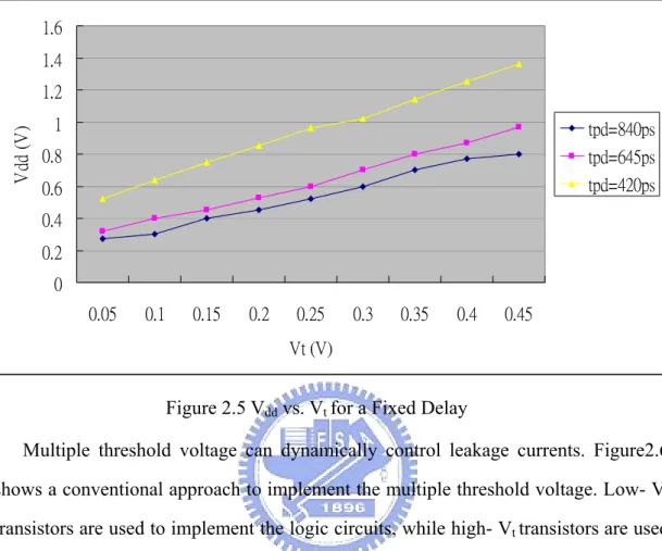
threshold devices, which increase exponentially with decreasing Vt. Figure2.5 shows
the relationship that Vdd versus Vt while keeping the performance constant.
0 0.2 0.4 0.6 0.8 1 1.2 1.4 1.6 0.05 0.1 0.15 0.2 0.25 0.3 0.35 0.4 0.45 Vt (V) Vd d (V ) tpd=840ps tpd=645ps tpd=420ps
Figure 2.5 Vdd vs. Vt for a Fixed Delay
Multiple threshold voltage can dynamically control leakage currents. Figure2.6 shows a conventional approach to implement the multiple threshold voltage. Low- Vt
transistors are used to implement the logic circuits, while high- Vt transistors are used
as switches between the main circuit to Vdd and between the main circuit to ground.
The high-Vt transistors are cut-off during sleep (standby) periods, since the
subthreshold leakage can be largely reduced. During active periods, the high-Vt
transistors are turned on and the circuits works normally.
2.4.4 Adaptive Voltage Scaling (AVS)
In recent years, adaptively control the voltage or the threshold voltage has been emphasized, and gaining more and more attention. Figure2.7 shows the relationship of frequency vs. power of both adaptive voltage scaling (AVS) and adaptive body bias (ABB)[7]. Adaptively control the voltage means that the AVS system can locate the optimal voltage for the operating frequency. Whenever the frequency is changed, it sweeps the power supply for the optimal voltage of the new frequency. We can see in Figure2.7, the AVS operation sweeps the power supply at a reference frequency. Since the frequency indicates the performance which the designer wants, as long as it is not the highest performance of the design, the AVS system can locate a lower optimal voltage for the operating frequency. The difference between full swing voltage and the lower optimal voltage is the power which is saved by the AVS system.
The scheme of the conventional AVS system is shown in Figure 2.8. It is consists of a dc-dc converter, which a buck converter is used in the figure, a reference circuit, and a digital controller[8]. The reference circuit indicates the highest frequency at the regulated voltage, which is labeled as V in Figure2.8. the controller compare the reference frequency and the frequency output from the reference circuit, which is labeled as f in Figure2.8, and send the error along with the decision to the dc-dc converter. The buck converter is often used for a good efficiency dc-dc conversion, it converts the voltage to the voltage level that the controller indicates, and then applies the regulated voltage to the digital system.
Figure 2.8 Scheme of the Conventional AVS System[8]
2.4.5 Adaptive Body Bias (ABB)
Adaptive body biasing, which is shown in Figure 2.9, changes the threshold voltage dynamically by changing the substrate bias. It uses a lower threshold voltage to operate at low power supply voltage during active periods, and raise the threshold voltage during idle periods. Although the purpose is the same as using multiple threshold voltage, adaptive body biasing controls much better. The limitation of ABB
is that the threshold voltage changes in a square root with respect to source to bulk voltage and therefore a large voltage is required to change Vt , which also comes along
with increased parasitic capacitance.
Substrate
Voltage
Control
ABB.p
nWell
pWell
ABB.n
Vdd+3.3@standby
Vdd+0.5V@active
Vthp:<0.5V@standby
-0.27V@active
Vthn:<0.27V@active
>0.5V@standby
-0.5V@active
-3.3V@standby
Figure 2.9 Adaptive Body Biasing[9]
2.5 Dynamic Voltage Scaling
2.5.1 Essential Components
The dynamic voltage regulator consists of a detector , a loop filter, and a dc-dc converter. The frequency detector generates a digital error signal in proportion to the frequency error. This error is translated into an update signal for the dc-dc converter through the loop filter. The dc-dc converter provides the supply voltage Vdd ,
The voltage-controlled oscillator (VCO) is intergrated together with the circuit, and designed to match its critical path. The loop forces the output frequency of the VCO to equal the commanded frequency, at an input voltage Vdd . The circuit is therefore
run at the minimum supply voltage, at which the state request can be met, resulting in the lowest achievable energy per operation while sustaining Vdd .
2.5.2 Improving Energy Efficiency
Figure2.10 Energy Efficiency Improvement
The possible energy efficiency improvement of DVS is illustrated in Figure2.10. Starting at the nominal Vdd , when the clock frequency fclk, is reduced, there is a
proportional decrease in throughput. When this is at constant Vdd, there is no
reduction in energy. However, if it is scaled lock-step with fclk , then the lower curve is
2.5.3 Fundamental Trade-off
The digital circuits generally operate at a fixed voltage, and require a regulator to control the supply voltage variation. Sometimes the digital circuit produces large current for which the regulator’s output capacitor supplies the charge. Hence, a large output capacitor on the regulator is desirable to minimize the ripple on Vdd . A large
capacitor also helps to maximize the regulator conversion efficiency by reducing the voltage variation at the output of the regulator. However, the voltage converter required for DVS is different from a standard voltage regulator because in addition to regulating voltage for a given clock frequency, it must also change the operating voltage when a new clock frequency is request. To minimize the speed and energy consumption of this voltage transition, a small output capacitor on the converter is desirable, in contrast to the supply ripple requirement. Thus, the fundamental trade-off in a DVS system is between good voltage regulation and efficiency dynamic voltage conversion. It is possible to optimize the size of the output capacitor to balance the requirements for good voltage regulation with the requirements for a good dynamic voltage conversion.
2.6 Conversion Efficiency
The efficiency of a voltage regulator is defined as:
Total
Power
Dissipatio
n
Load
to
Delivered
Power
=
η
(2.5)The buck converter is very efficient at voltage conversion, with efficiencies typically in the 90-95% range[10]. It can be designed methodically for a fixed operating voltage. The converter designed for a large range of voltage and current loads is difficult. Several techniques have been developed for the converter loop design to improve the efficiency over this broad range of operating conditions[10].
In addition to the supply ripple and conversion efficiency performance metrics of a standard voltage regulator, the DVS converter introduces two new performance metrics: transition time and transition energy/ For a large voltage change (Vdd1 ->
Vdd2), the transition time is :
1 2
2
dd dd MAX dd TRANV
V
I
C
t
>>
×
×
−
(2.6)where IMAX is the maximum output current of the converter, and the factor of 2
exists because the current is pulsed in a triangular waveform. In practice, tTRAN will be
slightly longer for a low-to-high voltage transition because the actual current changing Cdd is IMAX – Idd * Vdd . The energy consumed during this transition is:
2 1 2 2 dd dd dd TRAN
h
C
V
V
E
=
×
×
−
(2.7) Since both transition time and transition energy are proportional to Cdd ,minimizing Cdd , yields a faster and more energy-efficient voltage converter.
2.6.1 Limits to Reducing C
ddDecreasing Cdd reduces transition time, and by doing so increases the speed at
which the voltage changes, dVdd/dt. But decreasing Cdd increases supply ripple, which
in turn increases circuit energy consumption as shown in Figure 2.11. The increase is moderate at high Vdd, but begins to increase as Vdd approaches VT because the
negative ripple slows down the circuit so much that most of the computation is performed during the positive ripple, which decreases energy efficiency. For values of supply ripple above 10%, the processor can still operate properly, but the increased energy consumption of the processor outweighs the decreased transition energy consumption, degrading overall system energy-efficiency.
Figure 2.11 Energy Loss Due to Voltage Supply Ripple
Loop stability is another limitation on reducing capacitance. As Cdd is reduced
the pole frequency increases. As the pole approaches the sampling frequency, interaction with higher-order poles will eventually make the system unstable.
The third limitation is that low-voltage conversion efficiency scales down with Cdd. Since the DVS processor will ideally be operating most of the time at low voltage,
it is important to maintain reasonable low-voltage conversion efficiency.
Increasing the converter sampling frequency will reduce the supply ripple and increase the pole frequency due to the sample delay. Thus, these two limits are not fixed, but can be varied. However, increasing the sampling frequency has two negative side-effects. First, low-load converter efficiency will decrease because the converter loop will need to be activated more frequently to maintain the same voltage. Second, the fCLK quantization error will increase. These side-effects may be mitigated
with a variable sampling frequency that adapts to the system power requirements .
hard constraint because system failure can be induced, but occurs for a much smaller Cdd than the supply ripple and stability constraints. Low-voltage conversion efficiency
is a soft-constraint, but cannot be improved by adjusting the converter sampling frequency.
2.7 Design Constraints Over Voltage
A typical circuit targets a fixed supply voltage, and is designed for ±10% maximum voltage variation. In contrast, a DVS circuit must be designed to operate over a much wider range of supply voltages, which impacts both design implementation and verification time.
2.7.1 Circuit Design Constraints
To realize the full range of DVS energy efficiency, only circuits that can operate all the way down to should be used. NMOS pass gates are often used in low-power design due to their small area and input capacitance. However, they are limited by not being able to pass a voltage greater than
Th
V
dd thn
V −V , such that a
minimum of is required for proper operation. Since throughput and energy consumption vary by 4x over the voltage range to
dd
V 2⋅VTh
Th
V 2⋅VTh, using NMOS pass gates
restricts the range of operation by a significant amount, and are not worth the moderate improvement in energy efficiency. Instead, CMOS pass gates, or an alternate logic style, should be utilized to realize the full voltage range of DVS. As previously demonstrated in Figure 3.1, the delay of CMOS circuits track over voltage such that functional verification is only required at one operating voltage. The one possible exception is any self-timed circuit, which is a common technique to reduce energy consumption in memory arrays. If the self-timed path layout exactly mimics that of the circuit delay path as was done in the prototype design, then the paths will scale similarly with voltage and eliminate the need to functionally verify over the entire range of operating voltages.
2.7.2 Circuit Delay Variation
While circuit delay tracks well over voltage, subtle delay variations exist and do impact circuit timing. To demonstrate this, three chains of inverters were simulated whose loads were dominated by gate, interconnect, and diffusion capacitance respectively. To model paths dominated by stacked devices, a fourth chain was simulated consisting of 4 PMOS and 4 NMOS transistors in series. The relative delay variation of these circuits is shown in Figure 2.12 for which the baseline reference is an inverter chain with a balanced load capacitance similar to the ring oscillator.
Figure 2.12 Relative CMOS Circuit Delay Variation over Supply Voltage
The relative delay of all four circuits is a maximum at only the lowest or highest operating voltages. This is true even including the effect of the interconnect’s RC delay. Since the gate dominant curve is convex, combining it with one or more of the other effects’ curves may lead to a relative delay maximum somewhere between the two voltage extremes. However, all the other curves are concave and roughly mirror the gate dominant curve such that this maximum will be less than a few
percent higher than at either the lowest or highest voltage, and therefore insignificant. Thus, timing analysis is only required at the two voltage extremes, and not at all the intermediate voltage values.
As demonstrated by the series dominant curve, the relative delay of four stacked devices rapidly increases at low voltage. Additional devices in series will lead to an even greater increase in relative delay. As supply voltage increases, the drain-to-source voltage increases for the stacked devices during an output transition. For the devices whose sources are not connected to or ground, their body-effect increases with supply voltage, such that it would be expected that the relative delay would be a maximum at high voltage. However, the sensitivity of device current and circuit delay to gate-to-source voltage exponentially increases as supply voltage goes down. So even though the magnitude change in gate-to-source voltage during an output transition scales with supply voltage, the exponential increase in sensitivity dominates such that stacked devices have maximum relative delay at the lowest voltage. Thus, to improve the tracking of circuit delay over voltage, a general design guideline is to limit the number of stacked devices, which was four in the case of the prototype design. One exception to the rule is for circuits in non-critical paths, which can tolerate a broader variation in relative delay. Another exception is for circuits whose alternative design would be significantly more expensive in area and/or power (e.g. memory address decoder), but the circuits must still be designed to meet timing constraints at low voltage.
dd
V
2.7.3 Noise Margin Variation
Figure 2.13 demonstrates the two primary ways that noise margin is degraded. The first is capacitive coupling between an aggressor signal wire that is switching and an adjacent victim wire. When the aggressor and victim signals have the same logic level, and the aggressor transitions between logic states, the victim signal can also incur a voltage change. If this change is greater than the noise margin,
the victim signal will glitch and potentially lead to functional failure. Supply bounce is induced by switching current spikes on the power distribution network, which has resistive and inductive losses. If the gate’s output signal is the same voltage as the supply that is bouncing, the voltage spike transfers directly to the output signal. Again, if this voltage spike is greater than the noise margin, glitch, and potentially functional failure, will occur.
Figure 2.13 Noise Margin Degradation
For the case of capacitive coupling, the amplitude of the voltage spike on the victim signal is proportional to to first order. As such, the important parameter to analyze is noise margin divided by to normalize out the dependence on . Figure 2.11 plots two common measures of noise margin vs. , the noise margin of a standard CMOS inverter, and a more pessimistic measure of noise margin,
. The relative noise margin is a minimum at high voltage, such that signal integrity analysis to ensure there is no glitch only needs to consider a single value of . If a circuit passes signal integrity analysis at maximum , it is guaranteed to pass at all other values of . dd V dd V dd V Vdd Th V dd V dd V dd V
Figure 2.14 Noise Margin vs. Supply Voltage
Supply bounce occurs through resistive (IR) and inductive (dI/dt) voltage drop on the power distribution network both on chip and through the package pins. Figure 2.15 plots the relative normalized IR and dI/dt voltage drop as a function of . It is interesting to note that the worst case condition occurs at high voltage, and not at low voltage, since the decrease in current and dI/dt more than offsets the reduced voltage swing. Given a maximum tolerable noise margin reduction, only one operating voltage needs to be considered, which is maximum . to determine the maximum allowed resistance (R) and inductance (L). The global power grid and package must then be designed to meet these constraints on resistance and inductance.
dd
V
dd
V
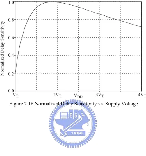
2.7.4 Delay Sensitivity
Supply bounce has another adverse affect on circuit performance in that it can induce timing violations. Supply bounce decreases a transistor’s gate drive, which in turn increases the circuit delay. If this increase occurs within a critical path, a timing violation may result leading to functional failure. A typical microprocessor uses a phase-locked loop to generate a clock frequency which is locked to an external reference frequency and independent of on chip voltage variation. As such, both global and local voltage variation can lead to timing violations if the voltage drops a sufficient amount to increase the critical paths’ delay past the clock cycle time. However, in the DVS system, the clock signal is derived from a ring oscillator whose output frequency is strictly a function of , and not an external reference. As such, global voltage variations not only slow down the critical paths, but the clock frequency as well such that the processor will continue operating properly. Localized supply variation, however, may only effects the critical paths, and not the ring oscillator. These can lead to timing violations if the local supply drop is sufficiently large. As such, careful attention has to be paid to the local supply routing. For the prototype design, a design margin of 5% was included in the timing verification to allow for localized voltage drops. Delay sensitivity is the relative change in delay given a drop in , and can be calculated as:
dd V dd V ⎟⎟ ⎠ ⎞ ⎜⎜ ⎝ ⎛ Δ ⋅ ∂ ∂ = ∂ → Δlim ( ) ) ( 0 Delay Vdd Vdd Vdd Delay Vdd Delay Delay Vdd ( 2.8)
This equation can be analytically quantified using Equation 2.8, and the nor
dd
malized delay sensitivity is plotted as a function of V in Figure 2.13. For dd
sub-micron CMOS processes, the delay sensitivity peaks at approximately 2 V⋅ . Thus, the design of the local power grid only needs to consider one value of V ,
Th
2 V⋅ , to ensure that the resistance/inductance voltage drop meets the design margin
ay variation. If the power grid meets timing constraints at this value of V , it is
Th
guaranteed to do so at all other voltages.
Chapter 3
oltage Scaling
Adaptive V
aptive supply voltage regulation reduces power and energy consumption by low
.1 Components of Adaptive Voltage Regulation
Ad
ering the supply voltage to the minimum which is required to support the operating frequency. On the other hand, it maximizes the energy efficiency of the circuits. Whenever the maximum performance is not required, the supply voltage can be scaled down so that the critical path can still meet the timing constraints. Hence, the power can be significantly reduced due to the quadratic dependency between the supply voltage and power.
3
In order to adaptively control the supply voltage, three essential components are required. A critical path emulator accurately predicts the performance of critical path at the regulated supply voltage, if the regulated voltage is not high enough for the critical path to meet the timing constraints, then the supply voltage is supposed to be raised. On the contrary, if the performance is better than expected, the supply voltage can be scaled down more. The other component of adaptive voltage regulation is a controller. The controller receives the result of the critical path emulator, and then compares the result to the expected performance. The output of the controller is transferred to the voltage converter, it contains the decision, which is scaling up the voltage or scaling down it, after the comparison and it also contains the error which gives voltage converter the information of the factor of scaling operation. A dc-dc converter is often used in voltage regulation, as a voltage converter, good energy efficiency is required to save more power than loss. The scheme is illustrated in Figure 3.1, the regulated voltage is transmitted to both the controller and the application. The controller outputs the up/down signal and the error to the dc-dc converter according to the predicted frequency generated by the critical path emulator which indicates the performance at the regulated voltage. The details of these components will be illustrated in next few sections.
3.2 Voltage Converter
The purpose of a voltage converter is to supply a regulated DC output voltage. dc-dc converters are commonly used in applications requiring regulated DC power, such as computers, medical instrumentation and communication devices.
3.2.1 Pulsed Width Modulation (PWM) Operation
Basic dc-dc converters such as buck, boost, and buck-boost converters are similar in that they each have two complementary switches and one inductor. Their conversion ratios may all be adjusted by using PWM to vary the duty cycle. The pulsed width modulation control technique maintains a constant switching frequency and varies the ratio of the charge cycle (time when the switch is on)) and the discharge cycle (time when the switch is off) as the load varies. Duty cycle can be represented as: t s control s on
V
V
T
t
D
=
=
(3.6) This technique offers high power efficiency. In addition, because the switching frequency is fixed, the noise spectrum is relatively narrow, allowing simple low-pass filter techniques to greatly reduce the peak-to-peak voltage ripple at the output. This is the reason why that PWM is popular in telecommunication application where noise interference is of concern. The circuit in Figure 3.2(a) shows a buck converter with a strictly resistive load and the switch mode, and its waveform is shown in Figure 3.2(b).Figure 3.2(b) Waveform of the Switching Mode Buck Converter
3.2.2 Buck Converter
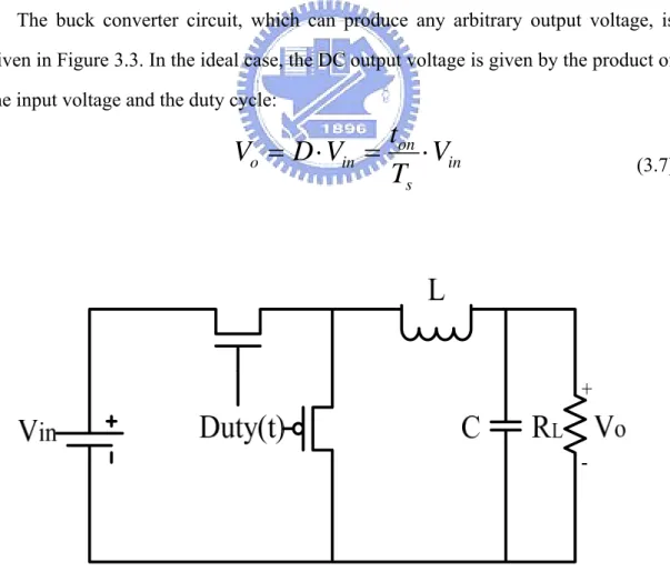
The buck converter circuit, which can produce any arbitrary output voltage, is given in Figure 3.3. In the ideal case, the DC output voltage is given by the product of the input voltage and the duty cycle:
in s on in o
V
T
t
V
D
V
=
⋅
=
⋅
(3.7)3.2.3 Boost Converter
The boost converter circuit, which can produce any arbitrary output voltage Vo≧
Vin, is given in Figure 3.4. In one portion of cycle, (1 - D), the NMOS device is on,
and the input voltage is applied across L, building up current and thus storing energy in the inductor. When the NMOS switch is turned off, the attempt to interrupt the current in the inductor causes the voltage rise rapidly. The PMOS device is turned on at this point, limiting the voltage produced by this inductive kick to the voltage on the output capacitor. During the fraction of the cycle, D, that the PMOS device conducts, some of the energy stored in the inductor is transferred to the output, along with additional energy flowing from the input. The cycle then repeats. The input and output voltages are related by:
o s on o in
V
T
t
V
D
V
=
⋅
=
⋅
(3.8)3.2.4 Buck-Boost Converter
The operation of the buck-boost converter is similar to that of the buck converter, in that the cycle starts with the input voltage applied across the inductor, in this case through the PMOS device for a duration. However, when the PMOS device is turned off, the circuit produces an output voltage polarity opposite to that of the input Figure 3.5. The energy transferred to C during this portion, 1-D, of the cycle(while NMOS device conducts) is only the energy stored in the inductor, with none coming directly from the input. Setting the average voltage across the inductor equal to zero allows the conversion ratio to be found:
in o
V
D
D
V
⋅
−
=
1
(3.9)This allows the output voltage of smaller or larger magnitude than the input.
3.3 Reference Voltage Generator
3.3.1 Traditional Reference Voltage Generator
In order to scale down the supply voltage, we need a reference voltage generator to generate a stable voltage. Therefore, the most important thing in the reference voltage generator is that the reference voltage must independent of temperature and external supply voltage as possible. Figure 3.6 shows the traditional reference voltage generator circuit.
Figure 3.6 Traditional Reference Voltage Generator
In Figure 3.6, there are four stages in this architecture, voltage divider, reference voltage generator, voltage follower and output driver. M1~M3, M5, M7 and M8 are operated at saturation region. M4 and M6 are operated at linear region. Voltage follower is a differential amplifier. Output driver is a large PMOS providing large current to the logic circuit. Figure 3.7 shows the illustration of reference voltage
generator circuit.
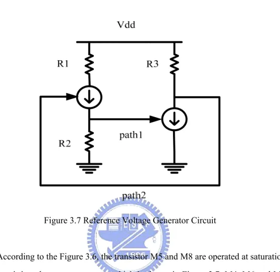
Figure 3.7 Reference Voltage Generator Circuit
According to the Figure 3.6, the transistor M5 and M8 are operated at saturation region, so it is to be a current source which is shown in Figure 3.7. M4, M6 and M7 are operated at linear region, so it is to be a resistor. In this reference voltage generator, there are two important paths, path1 (P1) and path2 (P2). P1 is a supply-independent skill to reduce the dependency between M2 current and supply voltage. P2 is a negative feedback compensation to increase the Vref stability. M5 and M8 are operated in saturation region to be a voltage control current source, so M5 and M8 will pull each other. On the other hand, it should be point out that in this reference voltage generator Vref > Vt (M5) + Vt(M8) must be satisfied.
3.3.2 Modified Variable Voltage Generator
In the adaptive voltage regulation, not only one voltage level is needed. Therefore, a modified scheme of the variable voltage generator is proposed. The modified
scheme is shown in Figure 3.8. Since the output of the reference voltage generator varies along with the value of R3 in Figure 3.8, we replace the transistor M7 with five paralleled transistors and a 5-bit control signal. After properly sized, these transistors can produce five different values of resistance. As the result, five different voltage levels can be produced. In this case, we set the five voltage levels to be 0.8V, 0.9V, 1.0V, 1.1V and 1.17V.
Figure 3.8 Modified Reference Voltage Generator
3.4 DC-DC Voltage Converter
The linear regulator is the basic building block of nearly every power supply used in electronics. Many efforts have recently been made to incorporate an on-chip dc-to-dc voltage converter into a high-density VLSI chip. This is because the power-supply voltage must be reduced to solve problems such as thermal cooling, power dissipation, and device reliability of a shorter channel MOS transistor. A straightforward approach to solve the above problem is to lower the supply voltage to below the traditional 1.2 V in accordance with the parts of chip that can accept the
lower supply voltage but at the same time does not degrade their performance.
A voltage regulator provides this constant DC output voltage and contains circuitry that continuously holds the output voltage at the design value regardless of changes in load current or input voltage (this assumes that the load current and input voltage are within the specified operating range for the part).
There are two kinds of voltage coverters have been widely used in modern VLSI chip. One is op-amp-based on chip dc-dc voltage converter. Another type of voltage converter that has traditionally been used in power systems is the switching mode circuit. Switching-mode voltage converter has high power efficiency but must use an LC filter that requires external parts. This is a main drawback of the switching-mode voltage converter. On the other hand, if the L and C components are integrated into the chip, the layout area will be very large and the accuracy is usually very poor. So, for a fully integrated solution, op-amp-based voltage converter shall be adopted.
A voltage converter for use in digital logic chips should have the following target specifications:
1. Low standby current so that the voltage converter consumes little power when on standby.
2. A small layout area.
3. A stable reduced internal supply voltage for a wide range of operation conditions.
The architecture of the on-chip voltage converter is shown in Figure 3.9. The basic blocks include a reference voltage generator, a differential-amplifier-based voltage follower, and an output driver circuit with low output impedance and high-driving capability. The function of the reference voltage generator is to produce a stable voltage that is free from fluctuations of and temperature. Because there are two
possible equilibrium points on the current source circuit, a voltage divider circuit is necessary. The voltage follower consists of a differential amplifier is to work as a gain stage in the voltage converter. Then, a nMOS transistor is used to work as a source follower and the output of the source follower is connected to the input of the differential amplifier to form a negative feedback system. This structure is very suitable for voltage converter when it is used in random logic circuits in terms of both drivability and layout.
Figure 3.9 The Architecture of On-chip Voltage Converter
3.4.1 Output Buffer
The voltage follower should have enough current supply capability and low output impedance so that the output voltage is not very much affected by the large loading current fluctuation. In the practical design, two kinds of follower s have been employed: n-type and p-type, both shown in Figure 3.10.
Figure 3.10 Differential Based Output Buffer
N-type has excellent phase margin, and therefore suitable for the logic chip concerning loop stability. The other type has been widely used in memory chips, because the storage capacitances of memory cells can be used to make the follower stable. For digital logic chip application, it should use n-type voltage follower. Since the voltage down converter should supply large current to logic gates which have large fluctuation of loading current, we attach a large-size nMOS transistor at the output as the driver to enhance drivability of this voltage down converter. On the other hands, it should be point out that in n-type voltage follower,
should be satisfied. The larger Vref is, the more the range of Vext is limited, though reference voltage generator allows a wide range. Therefore, selection of the voltage follower should be determined by its application and specific parameters.
Vext > Vout + Vtn
3.5 Simulation Result
The most important thing in reference voltage generator is that the reference voltage must be independent of temperature. Figure 3.11 shows the proposed voltage converter circuit. Five voltage levels can be produced by switching the “sel[4:0]”
signal. The simulation of each voltage versus the temperature is illustrated in Table 3.1.
Figure 3.11 The Proposed On-chip Voltage Converter Circuit
Voltage Level Vref(-25℃) Vref(25℃) Vref(100℃) Variation
1 1.17V 1.17V 1.15V -0.02V
2 1.10V 1.10V 1.07V -0.03V
3 1.01V 1.00V 0.96V -0.05V
4 0.92V 0.90V 0.82V -0.10V
5 0.82V 0.80V 0.70V -0.12V
Table 3.1 Temperature Variation
Table 3.2 and Table 3.3 show the simulation results of the modified Variable voltage generator.
Simulation Model TSMC 0.13um Temperature Variation (at 0.8V) 0.94 mV/°C Temperature Variation (at 1.17V) 0.16 mV/°C Average Power Consumption 1.73 mW
Output Loading 1uf/10k
Table 3.2 Simulation Result of the Modified Variable Voltage Generator
Output Voltage 1.17V 1.1V 1.0V 0.9V 0.8V Power Efficiency 78% 75% 70% 64% 58%
Table 3.3 Power Efficiency Simulation Results
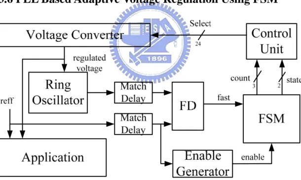
3.6 PLL Based Adaptive Voltage Regulation Using FSM
Figure 3.12 PLL Based Adaptive Voltage Regulator Using FSM
A scheme of PLL based adaptive voltage regulation is shown in Figure 3.12. It has a voltage-controlled ring oscillator as a critical path emulator, a phase lock loop (PLL) with a finite state machine (FSM) as the controller, and a variable reference voltage generator as a voltage converter.
3.6.1 Reference Circuit
Fig. 3.13 Reference Circuit
Figure 3.13 shows the reference circuit which is used in Figure 3.12. The frequency detector is composed of a voltage-controlled ring oscillator, a frequency detector. The ring oscillator operates at the regulated voltage, and indicates the highest performance of the critical path. The frequency detector compares the output of the ring oscillator and the reference frequency, and generates the “fast” signal to the finite state machine (FSM). If the “fast” signal becomes logic “1” means the output of the ring oscillator is higher than the reference frequency. The frequency detector consists of three connected D flip-flops with using the output of the ring oscillator as the clock inputs of the first two D flip-flops, and the reference frequency is used as the clock input of the last D flip-flip. The “fast” signal captured at the second cycle of the reference circuit is the right value. However, there may be some distance between the clock edge of the ring oscillator and the reference frequency at the first clock cycle. Hence, match delay elements in Figure 3.12 are placed between the ring oscillator and the frequency detector and between the reference frequency and the frequency detector.
3.6.2 Finite State Machine (FSM)
Figure 3.14 FSM
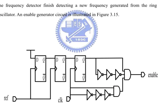
The finite state machine, which is shown in Figure 3.14, is a mechanism to determine if the voltage should be level up or level down according to the “fast” signal and enable. The voltage is determined to be level up if “fast” signal is at logic “0” when the enable rises, and is determined to be level down if “fast” signal is at logic “1” when the enable rises. Moreover, the voltage is determined to be locked in three conditions, if “fast” signal is at logic “0” when the first enable rises and then it changes to logic “1” when the next enable rises, or if “fast” signal is a logic “1” when the first enable rise and then it changes to logic “0” when the next enable rises, the
other condition is when the voltage level is at the top level (LV6) or at the bottom level (LV1), which can not be level up or level down anymore. In Figure 3.15, four states and the conditions are illustrated. ST0 is the initial state, when a logic “0” is detected, the voltage level count increases by one, and it goes to ST1. At ST1, it remains ST1 when a logic “0” is detected, if a logic “1” is detected or the voltage level count is 5 (LV6), it goes to ST3, which is the lock state. On the other side, when a logic “1” is detected at ST0, the voltage level count decreases by one, and it goes to ST2. At ST2, it remains ST2 when a logic “1” is detected, if a logic “0” is detected or the voltage level count is 0(LV1), it goes to the lock state, ST3. The finite state machine (FSM) determines the voltage level count, and then sends it to the control unit in Figure 3.12. However, and enable generator is needed to produce a pulse when the frequency detector finish detecting a new frequency generated from the ring oscillator. An enable generator circuit is illustrated in Figure 3.15.
Figure 3.15 Enable Generator
Chapter 4
Discrete Cosine Transform
The increase of the demand for high throughput portable digital equipment, with limited improvement in battery topology, has an increasing interest in low power systems. Since more and more functions are related to video information, video compression and decompression become an essential process to be done in digital devices. Discrete cosine transform (DCT) is frequently used in video compression. Many DCT algorithms were proposed in order to achieve high speed DCT.
4.1 Introduction to Discrete Cosine Transform (DCT)
The basic computation in a DCT-based system is the transformation of an 8 x 8 image block from the spatial domain to the DCT domain. The 1-D DCT transform is expressed as:
⎩
⎨
⎧
=
=
=
+
=
∑
=otherwise
k
k
c
k
k
i
x
k
c
z
o i i k,
1
0
,
2
/
1
)
(
7
,
,
3
,
2
,
1
,
0
,
16
)
1
2
(
cos
2
)
(
7K
π
(4.1)This equation can be represented in vector-matrix form as:
t
x
T
z
=
⋅
(4.2) where T is an 8 x 8 matrix whose elements are cosine functions. x and z are row and column vectors, respectively. The 8 x 8 matrix can be expressed as:⎥
⎥
⎥
⎥
⎥
⎥
⎥
⎥
⎥
⎥
⎥
⎦
⎤
⎢
⎢
⎢
⎢
⎢
⎢
⎢
⎢
⎢
⎢
⎢
⎣
⎡
−
−
−
−
−
−
−
−
−
−
−
−
−
−
−
−
−
−
−
−
−
−
−
−
−
−
−
−
=
g
e
d
b
b
d
e
g
f
c
c
f
f
c
c
f
e
b
g
d
d
g
b
e
a
a
a
a
a
a
a
a
d
g
b
e
e
b
g
d
c
f
f
c
c
f
f
c
b
d
e
g
g
e
d
b
a
a
a
a
a
a
a
a
T
(4.3) where⎥
⎥
⎥
⎥
⎥
⎥
⎥
⎥
⎥
⎥
⎥
⎥
⎥
⎥
⎥
⎥
⎦
⎤
⎢
⎢
⎢
⎢
⎢
⎢
⎢
⎢
⎢
⎢
⎢
⎢
⎢
⎢
⎢
⎢
⎣
⎡
=
⎥
⎥
⎥
⎥
⎥
⎥
⎥
⎥
⎥
⎦
⎤
⎢
⎢
⎢
⎢
⎢
⎢
⎢
⎢
⎢
⎣
⎡
16
7
cos
8
3
cos
16
5
cos
16
3
cos
8
cos
16
cos
4
cos
2
π
π
π
π
π
π
π
N
g
f
e
d
c
b
a
These coefficients approximate to real numbers as Table 4.1 shows.
Coef. Real Value Binary number
a 0.4904 0011 1111 b 0.4619 0011 1011 c 0.4157 0011 0101 d 0.3536 0010 1101 e 0.2778 0010 0100 f 0.1913 0001 1000 g 0.0975 0000 1100
Many algorithms replace the 8 x 8 matrix T with its decomposition matrixes. Since the even rows and the odd rows of the matrix T are symmetric, the 1-D DCT matrix can be rearranged as:
(4.3)
⎥
⎥
⎥
⎥
⎦
⎤
⎢
⎢
⎢
⎢
⎣
⎡
−
−
−
−
⎥
⎥
⎥
⎥
⎦
⎤
⎢
⎢
⎢
⎢
⎣
⎡
−
−
−
−
−
−
=
⎥
⎥
⎥
⎥
⎦
⎤
⎢
⎢
⎢
⎢
⎣
⎡
⎥
⎥
⎥
⎥
⎦
⎤
⎢
⎢
⎢
⎢
⎣
⎡
+
+
+
+
⎥
⎥
⎥
⎥
⎦
⎤
⎢
⎢
⎢
⎢
⎣
⎡
−
−
−
−
−
−
=
⎥
⎥
⎥
⎥
⎦
⎤
⎢
⎢
⎢
⎢
⎣
⎡
4 3 5 2 6 1 7 0 7 5 3 1 4 3 5 2 6 1 7 0 8 4 2 0x
x
x
x
x
x
x
x
a
c
e
g
c
g
a
e
e
a
g
c
g
e
c
a
z
z
z
z
x
x
x
x
x
x
x
x
f
b
b
f
d
d
d
d
b
f
f
b
d
d
d
d
z
z
z
z
The seven coefficients in the two matrixes in equation (4.3) are separated in to two groups, which d, b, f are used to compute z0 , z2 , z4 , z8 and the others are used to
compute z1 , z3 , z5 , z7 . Hence, this decomposition is widely used in most of the DCT
algorithms.
4.2 Alternative Implementation
There are alternative methods of implementing DCT. Some of them use fast algorithms to achieve high throughput, some use external memory such as ROM to reduce computation time. The only purpose of these methods is to reduce the number of multipliers used in DCT, since multiplication uses most of the computation time of DCT.
![Figure 2.1 Multiple Supply Voltage[5]](https://thumb-ap.123doks.com/thumbv2/9libinfo/8742215.204408/16.892.132.760.556.1111/figure-multiple-supply-voltage.webp)
![Figure 2.7 Frequency vs. Power of AVS and ABB[7]](https://thumb-ap.123doks.com/thumbv2/9libinfo/8742215.204408/20.892.180.706.518.1031/figure-frequency-vs-power-avs-abb.webp)
![Figure 2.9 Adaptive Body Biasing[9]](https://thumb-ap.123doks.com/thumbv2/9libinfo/8742215.204408/22.892.204.674.237.730/figure-adaptive-body-biasing.webp)