Efficiency enhancement of InGaN/GaN multiple quantum well solar
cells using CdS quantum dots and distributed Bragg reflectors
Yu-Lin Tsai
a,
Chien-Chung Lin*
b, Hau-Vei Han
a, Hsin-Chu Chen
a, Kuo-Ju Chen
a,
Wei-Chi Lai
c,
Jin-Kong Sheu
c, Fang-I Lai
d, Peichen Yu
a,
and Hao-Chung Kuo*
aa
Department of Photonics and Institute of Electro-Optical Engineering, National Chiao Tung
University, Hsinchu 30010, Taiwan, R.O.C.
b
Institute of Photonic System, College of Photonics, National Chiao-Tung University, Tainan
71150, Taiwan, R.O.C.
c
Institute of Electro-Optical Science and Engineering, National Cheng Kung University, Tainan
70101, Taiwan, R.O.C.
d
Department of Photonics Engineering, Yuan-Ze University, Taoyuan 32070, Taiwan, R.O.C.
Email address: [email protected] (Chien-Chung Lin),
[email protected] (Hao-Chung Kuo)
ABSTRACT
In recent year, InGaN-based alloy was also considered for photovoltaic devices owing to the distinctive material properties which are benefit photovoltaic performance. However, the Indium tin oxide (ITO) layer on top, which plays a role of transparent conductive oxide (TCO), can absorb UV photons without generating photocurrent. Also, the thin absorber layer in the device, which is consequent result after compromising with limited crystal quality, has caused insufficient light absorption. In this report, we propose an approach for solving these problems. A hybrid design of InGaN/GaN multiple quantum wells (MQWs) solar cells combined with colloidal CdS quantum dots (QDs) and back side distributed Bragg reflectors (DBRs) has been demonstrated. CdS QDs provide down-conversion effect at UV regime to avoid absorption of ITO. Moreover, CdS QDs also exhibit anti-reflective feature. DBRs at the back side have effectively reflected the light back into the absorber layer. CdS QDs enhance the external quantum efficiency (EQE) for light with wavelength shorter than 400 nm, while DBRs provide a broad band enhancement in EQE, especially within the region of 400 nm ~ 430 nm in wavelength. CdS QDs effectively achieved a power conversion efficiency enhancement as high as 7.2% compared to the device without assistance of CdS QDs. With the participation of DBRs, the power conversion efficiency enhancement has been further boosted to 14%. We believe that the hybrid design of InGaN/GaN MQWs solar cells with QDs and DBRs can be a method for high efficiency InGaN/GaN MQWs solar cells.
Keywords: InGaN multiple quantum well solar cells, quantum dots, luminescent down shifting, anti-reflection
1. INTRODUCTION
The based alloys have been extensively used in light-emitting diode and laser diode. In recent year, InGaN-based alloy was also considered for solar cells application owing to the favorable photovoltaics properties such as direct bandgap, high absorption coefficient at band edge (on order of 105cm-1), high carrier mobility, superior radiation
resistance, thermal stability [1-2], and, most important of all, the wide bandgap range of the InN/GaN alloy materials from 0.7eV to 3.4eV which covers almost all solar spectrum [3-4]. In addition, an over 60% in theoretical conversion efficiency of four-junction solar cells had been verified and the efficiency of tandem solar cells have been discovered to increase with the number of junction [5]. No matter how many junctions are contained in a tandem solar cell, it always requires junctions that possess bandgaps greater than 2 eV. However, very few materials possess bandgap over 2 eV [6]. InN/GaN alloy is one of the few materials that are adaptable under the criteria. Therefore, InN/GaN alloy can be a candidate for high efficiency tandem solar cell.
Nevertheless, there are still many challenges for InGaN-based photovoltaic devices. A large lattice mismatch between GaN and InN limits InGaN-based photovoltaic devices to have high indium composition active layer with large thickness for light absorption. Once the thickness of InGaN layer exceeds a critical thickness, there will be many unexpected
Physics, Simulation, and Photonic Engineering of Photovoltaic Devices II, edited by Alexandre Freundlich, Jean-Francois Guillemoles, Proc. of SPIE Vol. 8620, 86201M · © 2013 SPIE
CCC code: 0277-786X/13/$18 · doi: 10.1117/12.2005823 Proc. of SPIE Vol. 8620 86201M-1
defects which lead to the recombination centers [7]. In general, the critical thickness of In0.1Ga0.9N is around 100nm, and
decrease rapidly with increasing of indium composition [8]. The unexpected recombination centers increase the consumption rate of photo-generated electron-hole pairs further to degrade the photovoltaics performance. Due to crystal quality concern, although multiple quantum wells (MQWs) structure is suitable for solar cell absorber, the thin quantum-well absorber restricted by the epitaxial challenges has led to insufficient light absorption [9]. On the other hand, indium tin oxide (ITO) is usually deposited as a conducting and transparent layer, however ITO shows a high absorption coefficient at ultraviolet region without generating photocurrent. Therefore, a new approach for solving the insufficient light absorption and reducing the high absorption of ITO layer is needed to be developed.
In previous studies, there are many approaches demonstrated to improve the light harvesting of InGaN MQW solar cells, such as using ZnO or SiO2 sub-wavelength structure to realize the graded refractive index interface for reduction of
Fresnel reflection, and simultaneously, for achievement of light scattering effect [10]. In addition, silver nanoparticle was used to utilize the surface plasmonic effect further to increase light scattering effect [11]. However, both of the issues of high absorption at ultraviolet region due to ITO layer and the low external quantum efficiency due to the insufficient light absorption has not been solved. Back reflector which reflects the unused light back to the absorber layer can play an important role in thin film solar cells [12]. The advantages of distributed Bragg reflectors (DBRs) include high reflectance, controllable stop band, and controllable central wavelength. By choosing appropriate DBRs, the issue of low external quantum efficiency can be solved. In the past, QDs have been widely used in optoelectronic devices such as light emitting diodes (LEDs) and solar cells. Recently, the CdS quantum dots on the top of the solar cell device with luminescent down shifting (LDS) effect and anti-reflective characteristic has been demonstrated [13-14]. The luminescent down shifting effect can absorb light in ultraviolet region and emission the light into longer wavelength, thus the issue of high absorption at ultraviolet region of ITO layer can be solved.
In this work, we successfully demonstrated a hybrid design InGaN/GaN MQWs solar cells utilizing colloidal CdS QDs and back-side DBRs to enhance the light harvesting of InGaN/GaN MQWs solar cells. The characteristics of InGaN/GaN MQWs solar cells with colloidal CdS QDs and back-side DBRs were measured by reflectance spectra, external quantum efficiency (EQE), and current density-voltage (J-V) profile.
2. EXPERIMENT
The InGaN/GaN MQW solar cell were grown by Metal-organic chemical vapor deposition (MOCVD) on c-plane sapphire substrate. The devices were composed with a 30-nm thick low temperature GaN nucleation layer and a 2-μm thick undoped GaN on sapphire substrate, 14 pairs In0.15Ga0.85N/GaN (3nm/5nm) undoped MQW sandwiched by a 2-um
thick Si-doped n-GaN layer (n-doping=2×1018 cm-3) and a 200-nm thick Mg-doped p-GaN (p-doping=2×1017 cm-3). A
110-nm thick indium-tin-oxide (ITO) p-GaN conducting layer was deposited by sputtering system. And then, the device were defined by 2x2 mm2 mesa using inductively coupled plasma reactive ion etching (ICP-RIE) system. Finally,
Cr/Pt/Au (50/50/1900nm) was deposited by electron-beam evaporation which serves as the p-GaN and the n-GaN contact metal.
The distributed Bragg reflector were composed of 11 pairs HfO2/SiO2 and grown by sputtering system at room temperature and deposited on the glass substrate. For controlling central wavelength and stop band of DBRs, the quartz was used to monitor during the process. Fig. 1(b) shows the measured reflectance spectra of 11 pairs HfO2/SiO2 DBRs, from wavelength of 385nm to 460nm, the reflectance is over 98%.
After regular semiconductor processes, the spin-coating method was used to form a CdS quantum dots thin film on the top of the device and DBRs was put at the back side of the device. The entire device structures are shown in Fig. 1(a).
Proc. of SPIE Vol. 8620 86201M-2
(a) Id
n
i 350 400 450Wave1
500 550 600.ngth (nm)
(h =nn
4iln :Hl 1N IP r 4411n444 I: 7,1111 =7,11 =Ililiiiiil -OW1
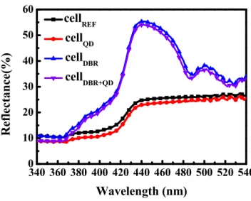
Figure 1. (a) reflectance sp Fig. 2(a) sh sharp rising photolumines nm. Fig. 2(b) solar cells. W and the diame CdS QDs, on Figure 2. (a) T The scanning The reflect and DBRs, an and without characteristic like CdS QD nanosphere-li index interfac Schematic of pectra of 11 pahows the abso edge was scence spectru ) shows the sc We can observe
eters are aroun ne with DBRs, The measured g electron micr tance spectra nd the referen QDs, the re c. The anti-ref Ds clusters. In ike CdS QDs ce and resultin InGaN/GaN M airs HFO2/SiO
orbance and p detected aro um was measu canning electr e the nanosph nd 80~100nm , one with both
d photolumine roscopic (SEM
3
of the InGaN nce bare cell a eflectance spe flection charac addition, bec clusters, acco ng in broadban MQW solar ce O2 DBRs. photoluminesc ound 400nm ured by the 3 ron microscop here-like struc m. Four kinds o h CdS QDs an escence (blue) M) image of th
3. RESUL
MQW solar c are shown in ectra illustrate cteristic of Cd cause the wav ording to the e nd anti-reflect ell structure w cence spectrum and the p 365 nm excita pic (SEM) ima cture on the su of InGaN/GaN nd DBRs, and ) and UV-Vis he CdS QDs oLT AND DI
cell with CdS Fig. 3(a). Wh e that CdS Q dS QDs can b velengths of i effective med tion character with CdS QDs ms of CdS QD peak absorpti ation, and a m age of the Cd urface which w N MQW solar d one bare cellabsorbance (b on the top of I
ISCUSSION
S QDs, the cel hen comparin QDs provide be caused by l incident photo dium theory, th istic for lightand DBRs. (b Ds in toluene.
on occurred major emission
dS QDs on the were the self-a r cells are prep as reference. black) spectra nGaN/GaN M
N
l with DBR, t g the reflectan a significant light scatterin ons are larger hese clusters p harvesting [21 b) The measur . In absorbanc at around n wavelength e top of InGaN assemble CdS pared for analof CdS QDs MQW solar ce
the cell with b nce spectra o t broadband ng effect of th r than the dim provides a gra 1]. red ce spectrum, a 380nm. The is around 410 N/GaN MQW S QDs clusters lysis: one with
in toluene. (b) lls.
both CdS QDs f the cell with anti-reflection he nanosphere mension of the aded refractive a e 0 W s h ) s h n -e e
Proc. of SPIE Vol. 8620 86201M-3
340 360 380 400 420 440 460 480 500 520 540 0 10 20 30 40 50 60
Refle
cta
nc
e(%)
Wavelength (nm)
cell
REFcell
QDcell
DBRcell
DBR+QDFigure 3. The measured reflectance spectra of InGaN/GaN MQW solar cell with CdS QDs, the cell with DBR, the cell with both CdS QDs and DBRs, and one bare cell as reference.
The measured photovoltaic current density-voltage (J-V) curves of the four types of InGaN/GaN MQW solar cells were performed under a simulated AM1.5G illumination condition and the results are shown in Fig. 4(a). The details of measured results are listed in Table 1. Compared to the reference cell, the short circuit current density (JSC) enhancement
of the cell with only CdS QDs and the cell with only DBRs are 5.5% and 16.5% respectively. With the combination of CdS QDs and DBRs, the enhancement in short circuit current density can be further boosted to 22%.
Sample Voc (V) Jsc (mA/cm2) F.F. (%) Efficiency (%)
Reference 1.35 1.09 56.03 0.83 QDs 1.34 1.15 54.52 0.85 DBR 1.37 1.27 56.19 0.98
QDs+DBR 1.37 1.33 54.79 1.002
Table 1. Current-Voltage Characteristics of of InGaN/GaN MQW solar cell with CdS QDs, the cell with DBR, the cell with both CdS QDs and DBRs, and one bare cell as reference.
Fig. 4(b) shows the measured external quantum efficiency (EQE) of the four types of InGaN/GaN MQW solar cells. The results of EQE can indicate the relationship between light absorption and photocurrent. The low EQE at the wavelengths shorter than 360nm can be attributed to several reasons, including junction depth, surface recombination, and absorption of ITO layer at UV regime. For the cell with only CdS QDs, there exhibits an overall EQE enhancement at a wavelength ranging from 350 nm to 440 nm which can be attributed to light scattering effect and anti-reflective characteristic of the nano-cluster CdS QDs on top. The results well agree with the reflectance spectra. It is noteworthy that, a significant enhancement at a wavelength ranging from 350 nm to 365 nm is observed from EQE of the cell with CdS QDs when comparing to that of reference cell. It is due to down conversion capability possessed by CdS QDs. As UV photons incident into the cell with CdS QDs on top, instead of being absorbed by ITO, they are absorbed by CdS QDs and then be converted into photons with longer wavelengths, therefore are able to penetrate through ITO layer without absorption and reach MQW absorber layer. To avoid incident photons being absorbed in ITO layer can suppress deterioration in EQE brought by the poor photon-generated carrier extraction efficiency of ITO and surface recombination in ITO layer. For the cell with only DBRs, there shows a significant EQE enhancement at a wavelength range of 380- 440 nm due to that the DBRs can reflect the photons back into MQW absorber layer and prolong the
Proc. of SPIE Vol. 8620 86201M-4
(a) N E E _ 2.2 2.0 1.8 V cellDBR cellQD +D]
l\
BR 340 36(I\\
10 400 420 g Wavelength --cellREFt cellQD
} cellD
BR-p-cell
QD+DBFLte
140 460 480 (nm)1
optical path significant br with both Cd Figure 4. (a) T efficiency (EQ DBRs, and on To further absorption is with CdS QD by AR charac 365 nm can b explained by surface which wavelengths 360nm indica Figure 5. The comparing to length furthe roadband enha S QDs and DB The measured QE) of InGaN ne bare cell as understand th introduced in Ds when comp cteristic of the be observed in the LDS of C h can be sever and reduce th ates the improe enhancemen reference cel er to enhance ancement at a BRs shows th d photovoltaic N/GaN MQW s reference. he influence n the followin paring to refer e CdS QDs, n n EQE. The d CdS QDs. Mo rely affected b he influence o ovement broug 34 0.95 1.00 1.05 1.10 1.15 1.20 1.25 1.30 1.35 Enh an cement Factor nt factors of bo ll. e the absorpti wavelength r e highest EQE c current densi solar cell with of CdS QDs ng. Fig. 5 show rence cell. Th ot the LDS ef difference betw ost of UV-pho by the surface of surface def ght by this CdS 40 360 W
oth EQE (blue
ion. By comb range of 350-4 E which transf ity-voltage (J-h CdS QDs, t(J-h on the InGaN ws the enhanc he enhanceme ffect of CdS Q ween CdS QD oton-generated e defects. The
fects and ITO S QD layer.
380 400
Wavelength EQEQD/E Absorptio
e line) and abs
bining the Cd 440nm. Comp forms into the
-V) curve (b) T he cell with D N/GaN MQW cement factors ent in absorpti QDs. A signifi Ds absorption d electron-hol presence of C O layer. In Fig 420 440 h (nm) QEREF onQD/Absorptio sorption (red l dS QDs and pared to other e highest JSC. The measured DBR, the cell w W solar cells, d s of both EQE ion of the lon icant peak at a spectrum and e pairs in sola CdS QDs can r g. 5, a strong 0 460 nREF
ine) of the cel
DBRs, the E r three kinds o d external qua with both CdS detail analysi E and absorpt nger waveleng a wavelength d EQE enhanc ar cells are lo re-emit photon g enhancemen ll with CdS Q EQE shows a of cell, the cel
antum S QDs and
is in EQE and tion of the cel gth is achieved
range of 350– cement can be ocated near the ns with longe nt peak around Ds when a ll d ll d – e e r d
Proc. of SPIE Vol. 8620 86201M-5
4. CONCLUSION
We successfully demonstrated a hybrid design of InGaN/GaN MQWs solar cells combined with colloidal CdS QDs and back side DBRs. The down-conversion and anti-reflective effects of CdS QDs enhance the EQE for light with wavelength shorter than 400 nm, and the back side DBRs have effectively reflected the light back into the absorber layer which result in a broad band EQE enhancement. Finally, the overall power conversion efficiency enhancement as high as 7.2% compared to the device without assistance of CdS QDs. With the participation of DBRs, the power conversion efficiency enhancement has been further boosted to 14%.
REFERENCES
[1] O. Jani, I. Ferguson, C. Honsberg, S. Kurtz, Design and characterization of GaN/InGaN solar cells, Applied Physics Letters 91 132117 (2007).
[2] A. David, M. J. Grundmann, Influence of polarization fields on carrier lifetime and recombination rates in InGaN-based light-emitting diodes, Applied Physics Letters 97 033501 (2010).
[3] J. Wu, When group-III nitrides go infrared: New properties and perspectives, Journal of Applied Physics 106 011101 (2009).
[4] J. Wu, W. Walukiewicz, K. M. Yu, W. Shan, and J. W. Ager III, Superior radiation resistance of In1-xGaxN
alloys: Full-solar-spectrum photovoltaic material system, Journal of Applied Physics 94 6477 (2003).
[5] D.J. Friedman, Progress and challenges for next-generation high-efficiency multi-junction solar cells, Current Opinion in Solid State and Materials Science 14 131–138 (2010).
[6] A. Yamamoto, Md. R. Islam, T. T. Kang, A. Hashimoto, Recent advances in InN-based solar cells: status and challenges in InGaN and InAlN solar cells, Physica Status Solidi (c) 7 1309-1316 (2010).
[7] M. Leyer, J. Stellmach, C. Meissner, M. Pristovsek, M. Kneissl, The critical thickness of InGaN on (0 0 0 1) GaN, Journal of Crystal Growth 310 4913–4915 (2008) .
[8] A. Luque, A. Martí, Increasing the Efficiency of Ideal Solar Cells by Photon Induced Transitions at Intermediate Levels, Physical Review Letters 78 5014–5017 (1997).
[9] E. Matioli, C. Neufeld, M. Iza, S. C. Cruz, A. A. Al-Heji, X. Chen, R. M. Farrell, S. Keller, S. DenBaars, U. Mishra, S. Nakamura, J. Speck, and C. Weisbuch, High internal and external quantum efficiency InGaN/GaN solar cells, Applied Physics Letters 98 021102 (2001).
[10] J. Bai, T. Wang, S. Sakai, Influence of the quantum-well thickness on the radiative recombination of InGaN/GaN quantum well structures, Journal of Applied physics 88 4729 (2000)
.
[11] P. H. Fu, G. J. Lin, C. H. Ho, C. A. Lin, C. F. Kang, Y. L. Lai, K. Y. Lai, J. H. He, Efficiency enhancement of InGaN multi-quantum-well solar cells via light-harvesting SiO2 nano-honeycombs, Applied Physics Letters 100
013105 (2012).
[12] H. Sai, M. Kondo, Light trapping effect of patterned back surface reflectors in substrate-type single and tandem junction thin-film silicon solar cells, Solar Energy Materials & Solar Cells 95 131–133 (2011).
[13] H. C. Chen, C. C. Lin, H. V. Han, K. J. Chen, Y. L. Tsai, Y. A. Chang, M. H. Shih, H. C. Kuo, P. Yu, Enhancement of power conversion efficiency in GaAs solar cells with dual-layer quantum dots using flexible PDMS film, Solar Energy Materials & Solar Cells 104 92–96 (2012).
[14] C. C. Lin, H. C. Chen, Y. L. Tsai, H. V. Han, H. S. Shih, Y. A. Chang, H. C. Kuo, P. Yu, Highly efficient CdS-quantum-dot-sensitized GaAs solar cells, Optics Express 20 A319–A326 (2012).
Proc. of SPIE Vol. 8620 86201M-6