Improved performance of GaN based light emitting diodes with ex-situ sputtered AlN
nucleation layers
Shuo-Wei Chen, Heng Li, and Tien-Chang Lu,
Citation: AIP Advances 6, 045311 (2016); doi: 10.1063/1.4947299 View online: http://dx.doi.org/10.1063/1.4947299
View Table of Contents: http://aip.scitation.org/toc/adv/6/4 Published by the American Institute of Physics
Articles you may be interested in
Effect of strain in sputtered AlN buffer layers on the growth of GaN by molecular beam epitaxy AIP Advances 107, 032102032102 (2015); 10.1063/1.4927245
Improved performance of GaN based light emitting
diodes with ex-situ sputtered AlN nucleation layers
Shuo-Wei Chen,1,2Heng Li,1and Tien-Chang Lu1,a
1Department of Photonics, National Chiao Tung University, Hsinchu 300, Taiwan 2Epistar Corporation, Hsinchu 300, Taiwan
(Received 7 February 2016; accepted 11 April 2016; published online 18 April 2016)
The crystal quality, electrical and optical properties of GaN based light emitting diodes (LEDs) with ex-situ sputtered physical vapor deposition (PVD) aluminum nitride (AlN) nucleation layers were investigated. It was found that the crystal quality in terms of defect density and x-ray diffraction linewidth was greatly improved in comparison to LEDs with in-situ low temperature GaN nucleation layer. The light output power was 3.7% increased and the reverse bias voltage of leakage current was twice on LEDs with ex-situ PVD AlN nucleation layers. However, larger compressive strain was discovered in LEDs with ex-situ PVD AlN nucleation layers. The study shows the potential and constrain in apply-ing ex-situ PVD AlN nucleation layers to fabricate high quality GaN crystals in various optoelectronics. C 2016 Author(s). All article content, except where
oth-erwise noted, is licensed under a Creative Commons Attribution (CC BY) license (http://creativecommons.org/licenses/by/4.0/).[http://dx.doi.org/10.1063/1.4947299]
Solid state lighting based on GaN materials has evolved to be the most important general light-ing technology recently because of its high conversion efficiency, rigid structure and long lifetime.1,2
Crystal quality is always one of the most important factors which affect quantum efficiency in GaN based light-emitting diodes (LEDs). Due to the lack of natural GaN substrates, GaN-based LED structures are made typically on the (0001) c-plane sapphire substrates.3,4 The interfacial energy difference between sapphire and GaN could cause large amount of dislocations and low crystal quality of the subsequently grown GaN layer.5The degraded quality of GaN layers presents intensive nonradiative recombination centers severely reducing the efficiency.6For the purpose of decreasing the energy difference from lattice constant and thermal expansion coefficient mismatch between sapphire substrates and GaN, early pioneers applied in-situ low temperature AlN or GaN film to form the nucleation layer which provide a stable surface condition to grow the following bulk GaN.7,8This two-step growth has made great success and become foundation in realization
of commercial grade blue GaN-based LEDs. To further improve the GaN crystal quality, several growth methods, such as epitaxially lateral over-growth,9,10insertion of superlattice layers or SiN
x
nano–masks,11,12etc. had been proposed to reduce threading dislocation densities (TDDs). Among
them, patterned sapphire substrates (PSS) are then widely used on GaN based LEDs because the light extraction efficiency can be largely enhanced due to fluctuated interfaces between GaN and sapphire and the TDDs can be well controlled to a certain level to achieve high internal quantum efficiency (IQE).13
On the other hand, recently developed GaN free-standing substrates can provide excellent crystal quality and benefits of homo-epitaxy in making excellent optoelectronics.14However, high material costs of GaN substrates still hold back the popularity of utilizing the GaN substrates. More recently, ex-situ sputtered AlN nucleation layer on PSS has been demonstrated as a cost-effective way to improve the crystal quality and electrical properties of GaN epitaxy layers for GaN based LEDs.15The improve-ment could be due to the fact that ex-situ sputtered AlN nucleation layer has better coverage on sap-phire substrates and could lower the lattice constant mismatch between sapsap-phire and the GaN film.
aCorresponding author. E-mail address:[email protected]; Tel.:+886-3-5131234; fax: +886-3-5727981
045311-2 Chen, Li, and Lu AIP Advances 6, 045311 (2016)
Nevertheless, there still exists large difference of lattice constant and thermal expansion coefficient between GaN and sapphire substrate which leads to large strain in the LED structure and formation of cracks. According to the strain-related quantum-confined Stark effect (QCSE), this strain can form internal electric field that induces band bending and suppress the recombination efficiency between electrons and holes in the multiple quantum wells (MQWs).16–18 Therefore, relationship of strain, crystal quality and electrical properties needs to be systematically studied.
In the present study, ex-situ AlN nucleation layer was deposited on 4-inch PSS by sputtered physical vapor deposition (PVD). Then, the GaN-based LED epitaxial structures were grown by metal organic chemical vapor deposition (MOCVD) followed by the process to form LED chips. The structural and optical characteristics of the as-grown wafers have been investigated and excel-lent crystal quality has been obtained for GaN films grown on the ex-situ sputtered AlN nucleation layer. On the other hand, the LED with AlN nucleation layer showed a higher strain within the structure. Finally, the improvement of electrical and optical properties can be observed at the LED samples with AlN nucleation layers.
The GaN based LED structures were grown on 4-inch (0001) PSS by MOCVD. Trimethyl-gallium (TMGa), trimethylaluminium (TMAl), trimethylindium(TMIn), and ammonia (NH3) were
used as precursors of chemical reactions for Ga, Al, In, and N sources, respectively. N-type and p-type doping sources were silane (SiH4) and bicyclopentadienyl magnesium (Cp2Mg), respectively.
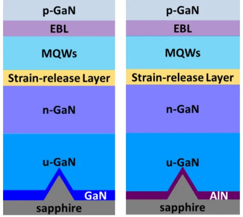
From Fig. 1, for sample A, a conventional in-situ 25-nm-thick low temperature GaN (LT-GaN) nucleation layer was deposited at 550 ◦C on PSS in MOCVD and the sample B was deposited with an ex-situ 25-nm-thick PVD AlN nucleation layer. After that, the same GaN based LED struc-tures grown on both samples consisted of a 4-µm-thick unintentionally doped GaN (u-GaN) layer, 3-µm-thick n-type GaN layer (n-doping = 1 x 1019 cm−3), 900-Å-thick strain-release layer, nine
pairs of InGaN/GaN MQWs with a 3-nm-thick un-doped well and a 12-nm-thick n-doping barriers as active regions, a 60-nm-thick p-type Al0.1Ga0.9N (p-doping= 8 x 1019cm−3) electron blocking
FIG. 1. Schematic diagram of LED structures with an in-situ LT GaN nucleation layer (sample A) and an ex-situ PVD AlN nucleation layer (sample B). The diameter, space, and height of cone on PSS were 2.8, 0.2, and 1.8 µm, respectively.
layer (EBL), and a 100-nm-thick p-type GaN cap layer (p-doping = 1 x 1019 cm−3). The crystal
qualities of sample A and B were analyzed by scanning electron microscope (SEM), transmission electron microscope (TEM), and high resolution X-ray diffraction (HRXRD). The optical properties of the InGaN/GaN MQWs were investigated by measuring power-dependent photoluminescence (PL) at low and room temperature. The excitation source was a 400 nm laser light, second harmon-ically generated from a Ti-sapphire pulse laser (Mira 900), to determine the power-dependent IQE. The efficiency was defined as the photon numbers emitted from the sample divided by the excitation photon numbers.19The strain distribution of the thin film structure was investigated by measuring
depth resolved Raman spectra.20The excitation source was a 532 nm laser light and the scattered
light was collected by a 100x, NA0.7 objective lens. To perform depth-resolved Raman measure-ment, the sample was mounted on a z-axis piezo stage to vary the laser focusing depth. Since the phonon frequency shift was linearly proportional to both the biaxial and uniaxial strain in GaN,21,22
the local strain can be evaluated by analyzing the Raman peak position. The fabricated LEDs had dimension of 26 x 30 mil.2The light output power-current-voltage (L-I-V) characteristics of LEDs were analyzed by a probe station and an integrated sphere instrument under CW operation at room temperature.
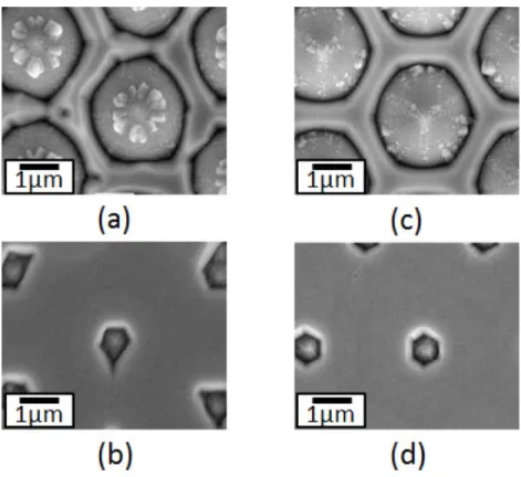
Fig.2shows the surface morphology of GaN grown on PSS with different nucleation layers for
growth time of 10 minutes and 25 minutes, respectively. With the in-situ LT-GaN nucleation layer in sample A [Fig.2(a)and2(b)], the growth of GaN was not only on the spacing area of c-plane region but also on the slope of cones. On the other hand, GaN layers of sample B with the ex-situ PVD AlN nucleation layer [Fig.2(c)and2(d)] have less GaN grains on the cone region. Moreover, Fig.2(c)
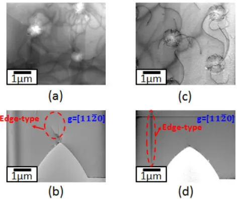
and 2(d) also show better crystalline edges forming perfect hexagonal-shape stacks. Therefore, ex-situ PVD AlN nucleation layer can offer a better coverage condition to enhance c-plane region growth and suppress cone region lateral growth.23,24Fig.3shows the plane view and cross-sectional TEM image of sample A and sample B. The screw dislocation density of sample A [Fig.3(a)] was
FIG. 2. SEM top view images of GaN epitaxial layer grown on PSS with an in-situ LT GaN nucleation layer after (a) 10 minutes and (b) 25 minutes growth, and that with an ex-situ PVD AlN nucleation layer after (c) 10 minutes and (d) 25 minutes.
045311-4 Chen, Li, and Lu AIP Advances 6, 045311 (2016)
FIG. 3. TEM images of GaN epitaxial layer grown on PSS: (a) and (b) with an in-situ LT GaN nucleation layer, (c) and (d) with an ex-situ PVD AlN nucleation layer. (a) and (c) were plane view TEM images around top of cones. (b) and (d) were the cross sectional TEM images. Screw dislocation density was estimated to be 1.22 #/µm2in (a) and 0.56 #/µm2in (c).
twice more than sample B [Fig.3(b)]. From the cross-sectional TEM image [Fig.3(b)and3(d)], stacking fault can be easily seen around top of patterns in sample A; however, there was almost no defects on the top region of cones in sample B. Moreover, in these two cross-sectional TEM images [Fig.3(b)and3(d)], the g vectors of samples A and B were both g=[11-20]. The edge-type dislocations were also identified in these two images, which were marked by red circles. In addition, the X-ray (102) full-width at half maximum (FWHM) could be reduced from 245 of sample A to 113 arcsec of sample B, and (002) FWHM was also from 228 to 106 arcsec. Based on these investigation, the crystal quality of GaN layers can be effectively improved by using the ex-situ PVD AlN nucleation layer.
The forward bias L-I-V results are shown in Fig.4(a). When the injection current density was 120 A/cm2 (injection current at 600 mA), the light output powers were 703 and 729 mW, while
the forward bias voltages were 3.87 and 3.85 V for sample A and sample B, respectively. The light output power (LOP) of sample B was 3.7 % higher than sample A. Furthermore, the forward voltage
of sample A was slightly higher than sample B indicating that the resistance caused by defects could also be decreased while the crystal quality was improved. Fig.4(b)shows the reversed bias leakage current. The reversed bias leakage current for sample A started at -6V, and that for sample B started at -14V. Moreover, the breakdown voltages of sample A and B were -51V and -59V, respectively. It is well-known that reversed bias leakage current closely depends on the dislocation density so that the better crystal quality would result in the lower leakage current. The L-I-V results again demonstrated the benefits of using the ex-situ PVD AlN nucleation layer.
Figs. 5(a) and5(b) show the PL emission peak and spectra FWHM of sample A and B as a function of excitation power, respectively. At the lower excitation power, the FWHM of PL emission peak decreased with the blue-shift of PL emission peak because the QCSE was gradually screened and the MQWs became flatter with increasing the carrier density. At the higher excitation power, the QCSE was completely screened and the Burstein–Moss effect started to dominate the blue-shift of PL emission peak.25Meanwhile, large amount of carriers were pushed to higher energy
states due to the fact that all states close to the conduction band are populated, so the FWHM of PL emission peak increased. The energy shift of PL emission peak of sample A and B before the FWHM raising were 8.0 and 15.5 meV, respectively. The energy shift result indicates that higher compressive strain could exist in the LED with the ex-situ PVD AlN nucleation layer. For the purpose of understanding strain distribution within the LED structure, the depth resolved confocal Raman spectroscopy was measured. The result in Fig.5(c)indicates that both samples were under compressive strain, because the E2
highRaman peak was higher than that of unstrained GaN bulk
occurred at 567.6 cm−1.21,22The Raman peak positions were 569.10 and 569.7 cm−1for sample A
and B, respectively. Fig.5(d)shows the peak position of GaN E2
highRaman peak as a function of
the sample depth, from the sample surface to the substrate interface. The error bars reflected the
FIG. 5. (a) and (b) Power dependent PL peak wavelength and FWHM as a function of excitation power for sample A and B, respectively. (c) The E2highRaman peak of sample A and sample B, respectively. (d) The Raman peak frequency shifts of the GaN E2highphonon modes of sample A and B are plotted as a function of the depth of epitaxial layer from the p-GaN surface toward the sapphire substrate.
045311-6 Chen, Li, and Lu AIP Advances 6, 045311 (2016)
uncertainty in the curve-fitting. There was partial strain release during the growth of GaN in sample A due to the generation of more defects so that the strain around the surface was lower than that in sample B. On the other hand, compressive strain in sample B was relatively high due to the more coherent growth by using the ex-situ PVD AlN nucleation layer. Despite a larger strain existed in sample B, it still possessed higher light output power and reverse breakdown voltage because of the better crystal quality.
Crystal quality of GaN layers was greatly improved with ex-situ PVD AlN nucleation layers owing to the fact that PVD AlN nucleation layer can suppress crystal growth on the cone area of PSS and effectively reduce the dislocation density of GaN layers compared with GaN layers on in-situ LT GaN nucleation layers. In addition, the LOPof LEDs with ex-situ PVD AlN nucleation
layers was increased 3.7% with a lower forward bias voltage. Furthermore, the voltage of reverse bias leakage current and breakdown voltage were significantly improved. Finally, larger compres-sive strain was found in LEDs with ex-situ PVD AlN nucleation layers through PL and depth resolved Raman measurement. Nevertheless, LEDs with ex-situ PVD AlN nucleation layers still possessed better performance on optical and electrical properties because of the excellent crystal quality in LEDs with ex-situ PVD AlN nucleation layers.
ACKNOWLEDGMENTS
The authors would like to gratefully acknowledge Crux Ou, Young Yang and Wei-Chih Wen at Epistar Corporation and Prof. S. C. Wang, and Prof. H. C. Kuo at National Chiao Tung University for technical support. This work has been supported in part by the MOE ATU program and in part by the Ministry of Science and Technology of Republic of China in Taiwan under contract numbers of NSC 102-2221-E-009-156-MY3, and MOST 104-2221-E-009-096-MY3.
1T. Mukai, M. Yamada, and S. Nakamura,Jpn. J. Appl. Phys., Part 138, 3976 (1999).
2T. Mukai, S. Nagahama, M. Sano, T. Yanamoto, D. Morita, T. Mitani, Y. Narukawa, S. Yamamoto, I. Niki, M. Yamada, S. Sonobe, S. Shioji, K. Deguchi, T. Naitou, H. Tamaki, Y. Murazaki, and M. Kameshima,Phys. Status Solidi A200, 52 (2003).
3S. Yoshida, S. Misawa, and S. Gonda,Appl. Phys. Lett.42, 427 (1983).
4X. H. Wu, P. Fini, E. J. Tarsa, B. Heying, S. Keller, U. K. Mishra, S. P. DenBaars, and J. S. Speck,J. Cryst. Growth189–190, 231 (1998).
5C. Sasaoka, H. Sunakawa, A. Kimura, M. Nido, A. Usui, and A. Sakai,J. Cryst. Growth189–190, 61 (1998). 6S. D. Lester, F. A. Ponce, M. G. Craford, and D. A. Steigerwald,Appl. Phys. Lett.66, 1249 (1995). 7H. Amano, N. Sawaki, I. Akasaki, and Y. Toyoda,Appl. Phys. Lett.48, 353 (1986).
8S. Nakamura, M. Senoh, and T. Mukai,Appl. Phys. Lett.62, 2390 (1993).
9S. Gradeˇcak, P. Stadelmann, V. Wagner, and M. Ilegems,Appl. Phys. Lett.85, 4648 (2004). 10S. Einfeldt, A. M. Roskowski, E. A. Preble, and R. F. Davis,Appl. Phys. Lett.80, 953 (2002).
11Z. Y. Li, M. H. Lo, C.T. Hung, S.W. Chen, T. C. Lu, H. C. Kuo, and S. C. Wang,Appl. Phys. Lett.93, 131116 (2008). 12J. Hertkorn, F. Lipski, P. Brückner, T. Wunderer, S.B. Thapa, F. Scholz, A. Chuvilin, U. Kaiser, M. Beer, and J. Zweck,J.
Cryst. Growth310, 4867 (2008).
13Y. J. Lee, J.M. Hwang, T. C. Hsu, M. H. Hsieh, M. J. Jou, B. J. Lee, T.C. Lu, H.C. Kuo, and S.C. Wang,IEEE Photon. Tech.
Lett.18, 1152 (2006).
14M. J. Cich, R. I. Aldaz, A. Chakraborty, A. David, M. J. Grundmann, A. Tyagi, M. Zhang, F. M. Steranka, and M. R. Krames,
Appl. Phys. Lett.101, 223509 (2012).
15C. H. Yen, W. C. Lai, Y. Y. Yang, C. K. Wang, T. K. Ko, S. J. Hon, and S. J. Chang,IEEE Photon. Technol. Lett.24, 294 (2012).
16J. H. Son and J. L. Lee,Opt. Express18, 5466 (2010).
17T. Wang, J. Bai, S. Sakai, and J. K. Ho,Appl. Phys. Lett.78, 2617 (2001).
18W. Z. Tawfik, J. Song, J. J. Lee, J. S. Ha, S.W. Ryu, H. S. Choi, B. Ryu, and J. K. Lee,Appl. Surf. Sci.283, 727 (2013). 19S. Watanabe, N. Yamada, M. Nagashima, Y. Ueki, C. Sasaki, Y. Yamada, T. Taguchi, K. Tadatomo, H. Okagawa, and H.
Kudo,Appl. Phys. Lett.83, 4906 (2003).
20W. L. Chen, Y. Y. Lee, C. Y. Chang, H. M. Huang, T. C. Lu, and Y. M. Chang,Rev. Sci. Instrum.84, 113108 (2013). 21V. Yu. Davydov, Yu. E. Kitaev, I. N. Goncharuk, A. N. Smirnov, J. Graul, O. Semchinova, D. Uffmann, M. B. Smirnov, A.
P. Mirgorodsky, and R. A. Evarestov,Phys. Rev. B58, 12899 (1998). 22H. Hiroshi,J. Phys.: Condens. Matter14, R967 (2002).
23Y. C. Chen, F. C. Hsiao, B. W. Lin, B. M. Wang, Y. S. Wu, and W. C. Hsu,J. Electrochem. Soc.159, D362 (2012). 24K. S. Lee, H. S. Kwack, J. S. Hwang, T. M. Roh, Y. H. Cho, J. H. Lee, Y. C. Kim, and C. S. Kim,J. Appl. Phys.107, 103506
(2010).
25J. Wu, W. Walukiewicz, W. Shan, K. M. Yu, J. W. Ager III, E. E. Haller, Hai Lu, and William J. Schaff,Phys. Rev. B66, 201403 (2002).