Design for Verification
THE HIGH COMPLEXITYof modern circuit designs has made verification the major bottleneck in the entire design process. There is an emerging need for a practical solution to the problem of verifying large designs. The recently proposed coverage-driven approach,1which uses some well-defined functional-coverage metrics2,3
to perform a quantitative analysis on simulation complete-ness, is rapidly becoming popular. Relying on coverage reports, verification engineers can focus on the untested areas and generate more patterns, using formal tech-niques or the designers’ knowledge to achieve better test coverage. Although 100% coverage still cannot guarantee a 100% error-free design, it provides a more systematic, efficient way to measure verification completeness.
It is not easy, however, to generate input patterns that satisfy coverage requirements for designs written in a hardware description language (HDL), especially for deep sequential designs. Certain descriptions in the designs could require execution of several hard-to-achieve conditions, such as specific state sequences. Without help from the original designers, it is hard for verification engineers to generate such input patterns.
The literature discusses several techniques for auto-matically generating functional test vectors for HDL designs.4,5Although these techniques do well on the combinational part of HDL designs, they are still not fea-sible for real designs, because they can become too
computationally expensive when deep state sequences are present. This diffi-culty resembles the major problem encountered in research on sequential automatic test-pattern generation.
A popular approach to this problem in manufacturing test is to insert some extra DFT circuits, such as test points or scan chains.6Adding these extra circuits can improve the testability of the whole design. Moreover, it can significantly reduce both the time needed to generate the required test patterns and the number of patterns needed to achieve the desired test coverage. This suggests that applying similar ideas to functional verification could enable an increase in simulation coverage and reduce verification time by the insertion of some design-for-verification (DFV) points into HDL designs.
Although DFT techniques have been well developed and widely used for many years, various differences between manufacturing test and functional verification prevent their direct application to functional verifica-tion. First, there’s the difference in operating levels. Because the fault model used in manufacturing test is defined at the gate level, most testing algorithms oper-ate at that level. However, the inputs of functional veri-fication problems are RTL descriptions. Obviously, functional-verification algorithms should be modified for running on high-level models the way DFT tech-niques are modified for use at the RTL.7-9
Second, the objectives are different. Manufacturing test checks for physical faults that occurred in the man-ufacturing process, so it focuses only on the netlist struc-tures. Functional verification, however, checks for design errors. Functional correctness is the main
con-A Design-for-Verification
Technique for Functional
Pattern Reduction
This technique reduces the number of required functional patterns by first defining conditions for hard-to-control (HTC) code in a hardware-description-language design and then using an algorithm to detect such code automatically. A second algorithm eliminates these HTC points by selecting a minimum number of nodes for control point insertion.
Chien-Nan Jimmy Liu, I-Ling Chen, and Jing-Yang Jou
However, some DFT circuits cannot be used in func-tional verification, because they might cause unex-pected functional errors after the test mode finishes. Therefore, functional verification requires carefully modified approaches to avoid such functional issues.
Third, the constraints are different. Engineers perform manufacturing test on the actual manufactured hard-ware, but functional verification occurs mostly through software simulation. Some limitations become unnec-essary in functional verification because the designs under test are not real hardware. For example, both con-trollability and observability6
should be considered in manufacturing test because access to the internal nodes is possible only through the primary inputs (PIs) and pri-mary outputs (POs). However, during functional verifi-cation, it’s possible to observe internal nodes in most software simulation environments with little overhead. In such cases, observability issues are less important.
Adding scan chains is also a popular DFT technique in manufacturing test. Although test time increases for shifting in the required values and shifting out the observed values one by one, this technique can reduce the extra overhead on the additional I/O pins present in real hardware. However, in functional verification, scan chains become unnecessary, because those extra pins will not incur real overhead. These differing constraints require suitable modifications.
With these considerations in mind, we propose an efficient DFV technique to help verification engineers reduce verification time. First we define conditions for hard-to-control (HTC) code in an HDL design, and then we propose an efficient algorithm to automatically detect such code. Along with HTC-code detection, we propose an algorithm that can eliminate those HTC points by selecting a minimum number of nodes on which to set up control points. These control points, or DFV points, are easily implemented through simulator support or by inserting extra code, and they provide greater control over a design’s internal nodes.
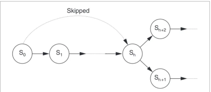
Enough controllability makes it easy to change a cir-cuit’s internal states by applying suitable values to the PIs and the DFV points. This capability lets verification engi-neers reduce the number of functional patterns. For example, if there’s a long state (S) sequence before a branch point, as shown in Figure 1, this preceding sequence will also be verified when branch 1 (Sn→ Sn+1)
is verified. After that, verifying branch 2 (Sn→ Sn+2)
requires going through the preverified state sequence again to reach the branch point for branch 2. In this case, the DFV points can change the internal states such that the preverified state sequence can be skipped. This great-ly reduces the number of required functional patterns, especially for deep sequential designs. Verification qual-ity remains high because only preverified functionalities are skipped. These operations only reduce existing func-tional patterns; they don’t generate any new patterns. The existing output values can produce the expected out-come without new computation, so the original response analyzer can still work by synchronously skipping the same number of clock cycles that were skipped at the inputs. Therefore, using our DFV techniques for func-tional pattern reduction incurs almost no quality degra-dation. Experiments show that the techniques reduce the number of functional patterns by an average of 37.7%.
HTC-code detection
Because the objectives in manufacturing test and functional verification are quite different, it’s necessary to redefine a suitable fault model and the testability measurement for functional verification before devel-oping the DFV techniques. The ability to observe the internal nodes during simulation means only control-lability issues must be considered in functional verifi-cation. However, it isn’t necessary to control the exact value of any net in a circuit when verifying functionali-ty. The concern is whether the HDL descriptions gener-ate correct results. Therefore, testability can be viewed as the ability to fire every code block during functional verification. Any hard-to-fire code blocks in the design are candidates for the application of DFV techniques to make them more testable.
Conditions of HTC code
In an HDL program, a triggering condition
deter-S0 S1 Sn
Sn+1
Figure 1. Applying design-for-verification (DFV) techniques makes it possible to skip preverified state sequences.
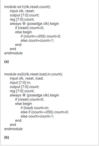
mines whether a description will execute. For example, in the Verilog code shown in Figure 2a, the description, count = count + 1, executes only when clk has a 0 → 1 transition, reset = 0, and count≠ 255, where the inter-section of these conditions is called the description’s triggering condition. Thus, a description is HTC if its trig-gering condition is HTC. Furthermore, because the val-ues of the variables associated with a condition
determine the condition’s result, the triggering condi-tion is HTC if the variables associated with it are HTC. Therefore, HTC code is that which has one or more HTC variables in the triggering conditions.
By this definition, HTC variables are those with HTC values. Propagating an arbitrary value for a variable from the PIs through some paths in the HDL code will make this variable controllable. If no such path exists for a able, it’s called an HTC variable. For example, the vari-able count in Figure 2a is an HTC varivari-able because it can be set only to a constant (0) and cannot propagate arbi-trary values to it. The variable count in Figure 2b, how-ever, is controllable because it can be set to any value while the input “load” of this design equals 1.
Extended S-graph
Using an S-graph10
extension—the extended S-graph (ESG)—to model the HDL design is the first step toward automatically detecting the HTC variables in an HDL design. In each hierarchy, a module, m, will have its own ESG, say Gm, which is a directed graph, Gm(V, E), where V = vertices and E = edges. The ESG contains six types of vertices, v∈ V; Table 1 shows the types and their mean-ings. This table defines sequential signals as the signals assigned in the edge-triggered process. Conditional state-ments represent the if or case statestate-ments. Functional blocks represent the other statements, except for condi-tional statements and statements involving constants only. All other vertices, except the M node, are single output. The edges between vertices represent the data dependency between them. Each directed edge, e(i, j) ∈ E, i and j ε V, means that node i is a fan-in of node j.
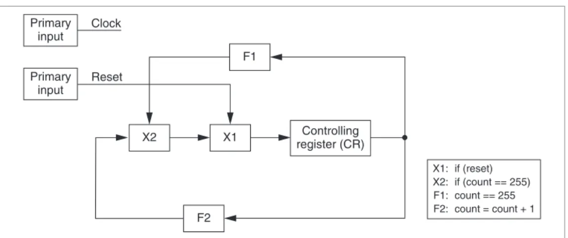
Building the corresponding ESG from HDL code is a simple assignment transformation. Figure 3 shows an ESG for the counter shown in Figure 2a. The corre-sponding assignments for the X and F nodes appear to the right of Figure 3. In this example, there are still two “count = 0” statements not shown in the ESG, because they are constant assignments and can be ignored in the following discussion. Therefore, multiplexers X1 and X2 in Figure 3 have only one data input, because the other input is from the “count = 0” assignment and can be omitted.
Sequential depth
The literature contains many definitions of controlla-bility in a circuit,6-9but they do not pertain to our appli-cation. Some definitions apply at the gate level and are not suitable at the RTL.6Others may be too complex for
Design for Verification
module ex1(clk,reset,count); input clk, reset;
output [7:0] count; reg [7:0] count;
always @ (posedge clk) begin if (reset) count=0; else begin if (count==255) count=0; else count=count+1; end end endmodule (a) module ex2(clk,reset,load,in,count); input clk, reset, load;
input [7:0] in; output [7:0] count; reg [7:0] count;
always @ (posedge clk) begin if (reset) count=0; else begin
if (load) count=in;
else if (count==255) count=0; else count=count+1; end
end endmodule
(b)
Figure 2. Verilog examples of hard-to-control (HTC) code (a) and controllable code (b). Table 1. The types of vertices in the extended S-graph (ESG) and their meanings.
Vertex type Meaning
PI Primary input
CR Controlling register (sequential signal that affects conditional statements)
NR Noncontrolling register (sequential signal that does not affect conditional statements)
X Conditional statement (multiplexer) F Functional block
represent the difficulty of controlling the value of the node’s output net in the ESG. In our definition, SD is the minimum number of registers encountered from the PIs to the current node. From another viewpoint, it’s the minimum number of clock cycles needed to propagate the required value from the PIs to the
current node. If a node’s SD is very large, it is often hard to control the node’s value directly from the PIs. Therefore, in our definition, if a node’s SD is infinite, its output net is recognized as an HTC variable.
Sequential-depth calculation
With a definition for the SD of each node (see the “Sequential-depth definitions for nodes” sidebar), it’s pos-sible to calculate the SD value of each node in the ESG, as
Because different types of vertices have different properties, there are different ways to calculate their sequential depths (SDs). Here we explain the equations and their meanings for the various types of vertices.
Node PI: SDPI= 0. It’s easy to assign any values to the pri-mary inputs without extra effort, so their SDs are set to 0.
Node CR, NR: SDCR,NR= SD(in) + 1. The SD is equal to the number of registers that the value passes in the path from the PIs to the node. Therefore, a register node’s SD should be incremented by 1 from its input SD to repre-sent the increased number of registers in the path. SD(in) means the SD value of its fan-in.
Node X: SDX= SDX_case1or SDX_case2. Because there are two possible cases for calculating the SD of an X node, we explain their different formulations and the conditions used in separate descriptions:
■ Case 1: SDX_case1= max {SD(in1), SD(in2), …}. If the
selection signal’s SD is larger than the SD values of all data inputs, the selection signal will dominate the output values. However, a value can still pass to its output if all input values are the same. This results in a shorter path to control the output values.
Therefore, the maximum value among the data inputs indicates that the output net can be set after the last input signal arrives.
■ Case 2: SDX_case2= max {min(SD(in1), SD(in2), …),
SD(select)}. If the selection signal’s SD is not larg-er than the SD values of the data inputs, the signal at the input with the smallest SD can be selected to pass the multiplexer in the shortest case. However, the signal can pass the multiplexer only when the selection signal has been controlled. Therefore, the minimum value from the data inputs and the maxi-mum value between it and the selection signal ensure that all required inputs can be ready before the number of clock cycles obtained in the formula results have elapsed.
Node F: SDF = max {SD(in1), SD(in2), …}. In the extended S-graph, all combinational assignments are represented as F nodes. In other words, only combina-tional operations exist in the F nodes. Therefore, although an F node’s exact function isn’t known, con-trolling all of its inputs enables control of its output. On the basis of this observation, the maximum value among the data inputs represents the SD value of the output net.
Sequential-depth definitions for nodes
Primary input Reset X2 X1 F2 X1: X2: F1: F2: if (reset) if (count == 255) count == 255 count = count + 1 Controlling register (CR)
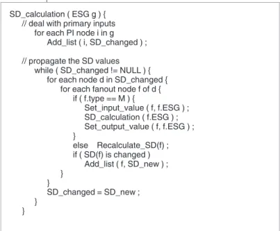
shown in the pseudocode of Figure 4. At the beginning, each node’s initial SD value is set to infinity. The initial SD values of PI nodes, however, are set to 0. After initial-ization, the SD_calculation( ) function propagates the SD values from PIs to internal nodes until each node’s SD value stabilizes. Relying on the definitions of the SDs makes it easy to determine the SD value of each node in the Recalculate_SD( ) function. Because the operations in this algorithm are similar to those in a breadth-first search, the complexity is the same as that of performing a breadth-first search—that is, O(V + E), where O is the order of complexity and V and E are the numbers of nodes and edges in all ESGs of the design.
If an M node is encountered, another ESG in the lower hierarchy must be traversed for the instantiated module. For each M node, the function Set_input_value( ) sets the current SDs at the node’s input nets as the initial SD val-ues of this module’s PI nodes. Then the calculation process can recursively traverse down one level and per-form the same calculation on the instantiated module’s ESG. When the calculations at lower hierarchies are com-plete, the returned SDs can set the SD values at the nodes’ output nets using function Set_output_value( ), and SD calculation of the nodes that follow the M node contin-ues. This strategy can solve the hierarchical issues in the HDL descriptions.
HTC-code elimination
There are many ways to make the HTC code in an HDL design more testable—for example, the
force-branching approach proposed by Hsu, Rudnick, and Patel.8However, not all these methods are useful in functional verification, because they can cause unex-pected functional errors. We therefore decided to use the value-controlling approach. With careful consider-ation of the loaded values, adding some control points to control the values of the HTC variables can drive the circuit to any known state without functional errors. Because the modified descriptions’ PIs can directly con-trol those variables, their SDs can be reduced.
Controlling node values
Some HDL simulators support special commands for directly controlling the values of any internal nodes, per-mitting control of the HTC variables without extra cost. If those commands are available, the DFV points can indicate where to fire the commands. However, not all HDLs and simulators support these commands.
When direct control of the internal variables’ values isn’t possible, inserting an extra input into the HDL code permits direct loading of the desired value into the HTC variable in test mode. Verification engineers can choose either of the two approaches, depending on their simu-lation environment.
Selecting nodes for DFV insertion
Typical HDL designs can contain many HTC vari-ables. Inserting a DFV point at every HTC variable will incur too much overhead in terms of simulation time. It’s better to try to eliminate all HTC variables with the fewest possible nodes selected for DFV point insertion. Generally speaking, controlling the values of all regis-ters in a design makes it possible to control the values of all other nodes. Therefore, only register nodes for controlling and noncontrolling registers (types CR and NR) should be considered for DFV point insertion.
Because only the variables in the conditional state-ments can influence an HDL design’s testability, the NR nodes do not contribute to testability improvement, so only the CR nodes must be considered for DFV inser-tion. Placing DFV points at every HTC CR node can eliminate all HTC variables in the design.
Actually, it isn’t necessary to insert DFV points for all HTC CR nodes, because the SDs of successor nodes might change when DFV points are inserted at their predecessor nodes. Carefully considering the func-tional dependencies between these nodes can pro-duce the same testability improvement with fewer inserted points. There are two cases in which the SDs of some CR nodes will be infinite. As Figure 5 shows,
Design for Verification
SD_calculation ( ESG g ) { // deal with primary inputs
for each PI node i in g Add_list ( i, SD_changed ) ; // propagate the SD values
while ( SD_changed != NULL ) { for each node d in SD_changed {
for each fanout node f of d { if ( f.type == M ) { Set_input_value ( f, f.ESG ) ; SD_calculation ( f.ESG ) ; Set_output_value ( f, f.ESG ) ; } else Recalculate_SD(f) ; if ( SD(f) is changed ) Add_list ( f, SD_new ) ; } } SD_changed = SD_new ; } }
they are classified as nonloop and loop cases. In nonloop cases, the register nodes have infinite SDs because they inherit the infinite SDs of predecessor reg-ister nodes. In these cases, eliminating the first node means that all subsequent nodes can be eliminated. Fortunately, it’s easy to recognize such source nodes because they have an obvious, unique property: no fan-in. All nodes, except for PI nodes, have at least one input in the ESG. If a node has no fan-in, its input must connect to a constant in the HDL descriptions; such a node is hard to control from the PIs. Therefore, select-ing the CR nodes without fan-in in the ESG to be the DFV insertion nodes makes it possible to eliminate all HTC registers belonging to the nonloop cases.
With the nonloop HTC registers eliminated, the remaining HTC registers then belong to the loop cases. So selecting one register in a loop to be the DFV inser-tion node permits eliminainser-tion of all HTC nodes in the same loop. Therefore, finding the minimum number of nodes in the ESG that can appear at least once in all loops formed by the HTC CR nodes amounts to finding the desired nodes at minimal cost. This problem is the same as the well-known cycle-breaking problem, which has many efficient algorithms proposed in the literature as solutions.11,12
These algorithms can directly obtain the optimal node selection.
In summary, there are two phases in the HTC-code elimination algorithm. The first deals with the nonloop
cases. Because the SDs of the nodes in the ESG may change after the DFV points are inserted, SD must be recal-culated to obtain the updated SD values. The second phase concerns the loop cases. The remaining HTC reg-isters in the ESG require a simplified S-graph. The vertices in the S-graph are the HTC CR nodes, and the edges in the graph represent the nodes’ functional dependencies. All other nodes in the ESG are simplified to the edges in the new S-graph; that is, along with their connections, these nodes become only a signal path in the new graph. Performing the cycle-breaking algorithm on this S-graph obtains the optimal selection of nodes for DFV insertion.
Experimental results
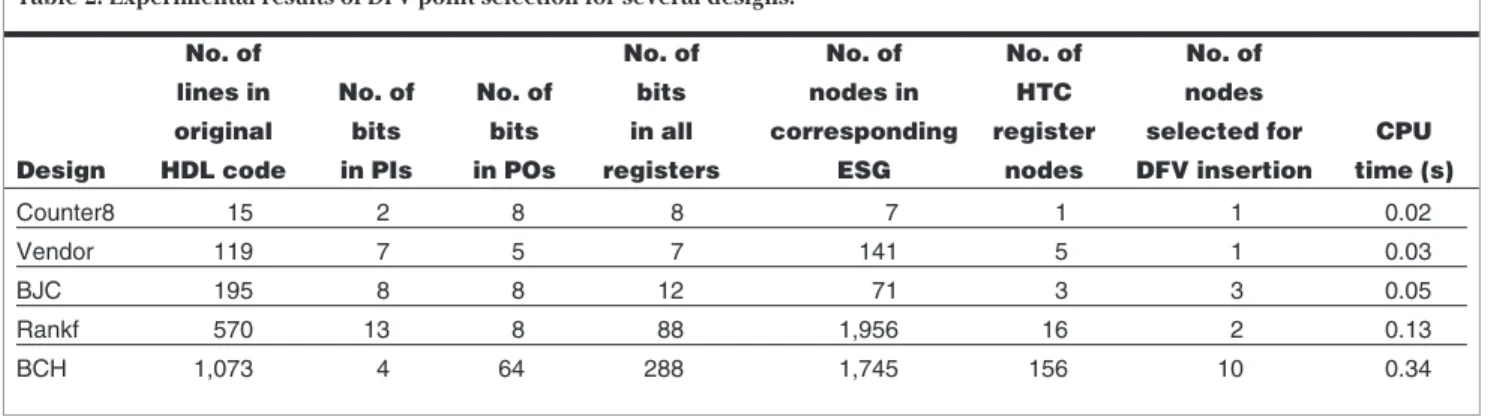
Table 2 shows the experimental results of HTC-code detection and elimination for several designs: an 8-bit counter (Counter8), a controller for a simple vendor machine (Vendor), a controller for a blackjack game machine (BJC), and a (63, 51) Bose-Chaudhuri-Hochquenghem–code decoder. The second-to-last row is for an 8 × 8 presorted rank filter (Rankf). This filter puts the last eight 8-bit data chunks in a register array according to their ranks in a way that permits observa-tion of the corresponding data at the output when users send the desired rank to the Sel input.
Following the proposed algorithms, we implement-ed the DFV selection tool in C++. The number of regis-ter nodes with infinite SDs, afregis-ter the SDs of all nodes
(a) (b)
Figure 5. Two cases of the controlling register nodes with infinite sequential depths: nonloop (a) and loop (b). Table 2. Experimental results of DFV point selection for several designs.
No. of No. of No. of No. of No. of lines in No. of No. of bits nodes in HTC nodes
original bits bits in all corresponding register selected for CPU Design HDL code in PIs in POs registers ESG nodes DFV insertion time (s)
Counter8 15 2 8 8 7 1 1 0.02 Vendor 119 7 5 7 141 5 1 0.03 BJC 195 8 8 12 71 3 3 0.05 Rankf 570 13 8 88 1,956 16 2 0.13 BCH 1,073 4 64 288 1,745 156 10 0.34
have been calculated, appears in the “No. of HTC reg-ister nodes” column. Having obtained the SDs, we per-formed the proposed selection algorithm to determine the number of selected nodes for DFV point insertion. As the results show, the number of HTC register nodes and the number of selected nodes aren’t always the same. This means the extra selection step is necessary to obtain a smaller set of selected nodes. The compu-tation time for total operations, performed on a 300-MHz UltraSparc II, appears in the last column of Table 2.
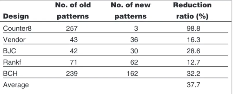
To demonstrate how the DFV techniques reduce the number of functional patterns, we performed another experiment on the same designs. The results appear in Table 3. For each design, we asked the designers to enhance their original functional patterns until the state-ment coverage achieved 100%, and the second column of Table 3 gives the old number of input patterns. After inserting the DFV points, we analyzed the original pat-terns and applied those points to skip the redundant state sequences, as shown in Figure 1, without losing any statement coverage. The number of new input pat-terns appears in the third column of Table 3. According to the reduction ratio, defined as (old – new)/old and appearing in the fourth column, the number of required functional patterns can be greatly reduced with an accompanying reduction in verification time.
SUCH REDUCTIONSin verification time can help verifi-cation engineers. Currently, we can use the proposed DFV techniques only to reduce the user-provided functional patterns, because we have not been able to find an auto-matic test-bench generator for functional verification. We will try to build one that supports the DFV techniques to the extent that initial pattern generation can also be skipped. At the same time, we will consider simulation overhead in our future improvements so that we can min-imize the extra cost our DFV techniques incur. ■
Acknowledgments
Partial support for this work by the R.O.C. National Science Council under grant NSC89-2218-E-009-060 is greatly appreciated.
References
1. A. Gupta, S. Malik, and P. Ashar, “Toward Formalizing a Validation Methodology Using Simulation Coverage,”
Proc. 34th Design Automation Conf. (DAC 97), ACM
Press, 1997, pp. 740-745.
2. D. Drako and P. Cohen, “HDL Verification Coverage,”
Integrated System Design, June 1998; http://www.
eedesign.com/editorial/1998/codecoverage9806.html. 3. J.-Y. Jou and C.-N. Liu, “Coverage Analysis Techniques
for HDL Design Validation,” Proc. 6th Asia Pacific Conf.
Chip Design Languages (APCHDL 99), ACM Press,
1999, pp. 3-10; http://www.ee.ncu.edu.tw/~jimmy/ publication.html.
4. K.-T. Cheng and A.S. Krishnakumar, “Automatic Func-tional Test Generation Using the Extend Finite State Machine Model,” Proc. 30th Design Automation Conf. (DAC 93), ACM Press, 1993, pp. 86-91.
5. F. Fallah, S. Devadas, and K. Keutzer, “Functional Vector Generation for HDL Models Using Linear Programming and 3-Satisfiability,” Proc. 35th Design Automation Conf. (DAC 98), ACM Press, 1998, pp. 528-533.
6. M. Abramovici, M.A. Breuer, and A.D. Friedman, Digital
Systems Testing and Testable Design, Computer
Science Press, New York, 1990.
7. S. Dey and M. Potkonjak, “Non-Scan Design-For-Testability of RT-Level Data Paths,” Proc. Int’l Conf.
Computer-Aided Design (ICCAD 94), IEEE CS Press,
1994, pp. 640-645.
8. F.F. Hsu, E.M. Rudnick, and J.H. Patel, “Enhancing High-Level Control-Flow for Improved Testability,” Proc.
Int’l Conf. Computer-Aided Design (ICCAD 96), IEEE CS
Press, 1996, pp. 322-328.
9. S. Dey, A. Raghunathan, and R.K. Roy, “Considering Testability during High-Level Design,” Proc. Asia and
South Pacific Design Automation Conf. (ASP-DAC 98),
IEEE Press, 1998, pp. 205-210.
10. K.-T. Cheng and V.D. Agrawal, “A Partial Scan Method for Sequential Circuits with Feedback,” IEEE Trans.
Computers, vol. 39, no. 4, Apr. 1990, pp. 544-548.
11. D.H. Lee and S.M. Reddy, “On Determining Scan Flip-Flops in Partial-Scan Designs,” Proc. Int’l Conf.
Computer-Aided Design (ICCAD 90), IEEE CS Press,
1990, pp. 322-325.
12. H.-M. Lin and J.-Y. Jou, “On Computing the Minimum Feedback Vertex Sets of a Directed Graph by
Contrac-Design for Verification
Table 3. Experimental results on functional pattern reduction. No. of old No. of new Reduction Design patterns patterns ratio (%)
Counter8 257 3 98.8 Vendor 43 36 16.3 BJC 42 30 28.6 Rankf 71 62 12.7 BCH 239 162 32.2 Average 37.7
Chien-Nan Jimmy Liu is an
assis-tant professor in the Department of Electrical Engineering at National Cen-tral University in Taiwan, R.O.C. His research interests include functional verification for HDL designs and verification of system-level integration. He has a BS and PhD in electronics engineering from National Chiao Tung University, Tai-wan, R.O.C. He is a member of Phi Tau Phi.
I-Ling Chen is a member of the
tech-nical staff at the SoC Technology Cen-ter of the Industrial Technology Research Institute, Taiwan, R.O.C. Her research interests include functional verification for HDL designs and RTL sign-off method-ology. She has a BS and MS in electronics engineer-ing from the National Chiao Tung University, Taiwan, R.O.C.
ing Department at National Chiao Tung University, Hsinchu, Taiwan. His research interests include behavioral logic, physical synthesis, design verification, and CAD for low power. He has a BS in electrical engineering from National Taiwan University and an MS and PhD in computer science from the University of Illinois at Urbana-Champaign. He is a member of Tau Beta Pi.
Direct questions and comments about this article to Jing-Yang Jou, Department of Electronics Engineering, National Chiao Tung University, Taiwan, R.O.C.; jyjou@ee.nctu.edu.tw.
For further information on this or any other computing topic, visit our Digital Library at http://computer.org/ publications/dlib.