國 立 交 通 大 學
電子工程學系 電子研究所碩士班
碩 士 論 文
用於 UWB 設計之 Viterbi 解碼器
Viterbi Decoder Design
for Ultra-Wide Band System.
研 究 生:蔡彥凱 Yan-Kai Tsai
用於 UWB 設計之 Viterbi 解碼器
Viterbi Decoder Design
for Ultra-Wide Band System
研 究 生:蔡彥凱 Student:Yan-Kai Tsai
指導教授:溫瓌岸 博士 Advisor:Dr. Kuei-Ann Wen
國立交通大學
電子工程學系 電子研究所碩士班
碩士論文
A Thesis
Submitted to the Institute of Electronics
College of Electrical Engineering and Computer Science
National Chiao Tung University
In Partial Fulfillment of the Requirements
For the Degree of Master of Science
In
Electronic Engineering
June, 2006
HsinChu, Taiwan, Republic of China
中華民國 九十五年六月
誌 謝
首先,第一個要感謝的是指導教授,溫瓌岸教授。感謝老師在兩年研究生涯 中,不斷的給予彥凱指導與督促。溫老師的循循教誨,讓學生在學習訓練的路途 上,能夠快速而正確的修正自己的研究方向,並且保持不鬆懈的心態進行研究。 也感謝 TWT_LAB 在這兩年中提供的豐富研究資源,讓我在研究上無後顧之憂。 感謝實驗室的學長們的指導與照顧:彭嘉笙,溫文燊,林立協,莊源欣,周 美芬,陳哲生,鄒文安。感謝兩年來一起打拚的同學:張懷仁,洪志德,賴俊憲, 游振威,廖俊閔,張書瑋,卓彥宏。還有實驗室的學弟帶來的快樂時光:林義凱, 莊翔琮,蘇建喻,吳家岱,梁書旗,李漢建,侯閎仁,蔡函霖。大家在生活上的 互相扶持與鼓勵,讓原本辛苦煩悶的研究工作,也變的輕鬆愉快許多。同時也要 感謝實驗室的助理:翁淑怡,楊怡倩,陳恩齊,陳慶宏,有妳們幫忙處理實驗室 的雜務,才能讓我們能夠專心致力於研究。 最後,感謝默默支持我的母親以及哥哥。你們不斷的支持與鼓勵,讓我覺得 更需要努力來回報你們。Viterbi Decoder Design
for Ultra-Wide Band System
Student: Yan-Kai Tsai Advisor: Dr. Kuei-Ann Wen
Department of Electronics Engineering Institute of Electronics
National Chiao-Tung University
Abstract
In this thesis, an IEEE 802.15.3a OFDM-based error correcting design and
implementation is presented. With the newly proposed arithmetic compare-select (CS),
the newly designed Viterbi decoder present good speed performance. According to
IEEE 802.15.3a, the convolutional code 1/3 is the base coding rate. Through the
puncture scheme, Viterbi decoder for the 802.15.3a standard can support several data
rates. We analyzed the soft decision resolution and traceback-length to get the
optimized solution between performance and complexity. The design flow and coding
scheme is based on IP qualification. The coding style, code coverage up to 100% and
other requirements are considered. Also, the macro design in CMOS.18μm is applied
誌 謝
首先,第一個要感謝的是指導教授,溫瓌岸教授。感謝老師在兩年研究生涯 中,不斷的給予彥凱指導與督促。溫老師的循循教誨,讓學生在學習訓練的路途 上,能夠快速而正確的修正自己的研究方向,並且保持不鬆懈的心態進行研究。 也感謝 TWT_LAB 在這兩年中提供的豐富研究資源,讓我在研究上無後顧之憂。 感謝實驗室的學長們的指導與照顧:彭嘉笙,溫文燊,莊源欣,周美芬,陳 哲生,鄒文安,林立協。感謝兩年來一起打拚的同學:張懷仁,洪志德,賴俊憲, 游振威,廖俊閔,張書瑋,卓彥宏。還有實驗室的學弟帶來的快樂時光:林義凱, 莊翔琮,蘇建喻,吳家岱,梁書旗,李漢建,侯閎仁,蔡函霖。大家在生活上的 互相扶持與鼓勵,讓原本辛苦煩悶的研究工作,也變的輕鬆愉快許多。同時也要 感謝實驗室的助理:翁淑怡,楊怡倩,陳恩齊,陳慶宏,有妳們幫忙處理實驗室 的雜務,才能讓我們能夠專心致力於研究。 最後,感謝默默支持我的母親以及哥哥。你們不斷的支持與鼓勵,讓我覺得 更需要努力來回報你們。Contents
中文摘要……..………..….I Abstract………..II 誌謝…….………..…...III Contents………..….IV List of Tables………..….VI List of Figures………..….VII Chapter 1 Introduction………...1 1.1 Introduction to Ultra-Wideband………...………...11.2 Ultra Wideband Physical Layer (802.15.3a)..……..………..…...2
1.3 OFDM Overview……..………..……...4
1.4 Design and Implementation Issue………...………..……...5
1.5 Organization of this thesis………..……..6
Chapter 2 Viterbi Decoder for Ultra-Wideband ………..……..…………..7
2.1 Design Requirements of Viterbi Codec for UWB………….…………..7
2.1.1 Scrambler……….………8
2.1.2 Convolutional encoder……….………8
2.1.3 Puncture ……..….…….……….……….9
2.1.4 Interleaving …..………...8
2.2 Viterbi Decoder Architecture………..………12
Chapter 3 ACS module with Arithmetic CS unit………...…...17
3.1 Deduction of Arithmetic CS unit ..………...……….……….……17
3.2 Arithmetic CS Circuit Analysis….……….…………...…..22
Chapter 4 Architecture of Viterbi Decoder.….………..…………..35
4.1 Depuncture Module ………….………..………..………36
4.2 Viterbi Decoder Module………..………...38
4.2.1 BMC Module………...…...…………..………....40
4.2.2 ACS Module………...…...………....41
4.2.2.1. Implementation ssues…………...…...………....42
4.2.2.2 ACS Overflow Preventaion…….…...………....43
4.2.3 Traceback Module ..………...…...………....44
4.2.4 Discussion between different Traceback Length………....46
Chapter 5 Implementation and Veriification………..……..……49
5.1 Introduction.….………..…...…….…49
5.2 System Co-simulation……….……….…51
5.3 RTL Design and soft IP Qualification………...………...…53
5.4 Function Verification………..….………...……….…55
5.5 Timing and Area analysis………..….………...……….…57
5.6 FPGA Prototyping………..….………...………….……….…58
Chapter 6 Conclusions and Future Work……….66
6.1 Conclusions………...………66
6.2 Future Work…..………...………67
List of Tables
Table 1.1: Rate-dependent parameters .….………..….…..2
Table 1.2: Timing-related parameters ………….……….3
Table 1.3: PHY layer timing parameters .………...3
Table 3.1: Relations Definition……….…….19
Table 3.2: All relations with four input data……….21
Table 3.3: Conditions of the Maximum Value……….……….………22
Table 3.4: Complexity of CS unit……….………..…………25
Table 3.5: Complexity of ACS unit……….………..…………31
Table 4.1: The mapping table of metrics by the correlation algorithm..………41
Table 4.2: Analysis of ACS architecture..……….………42
Table 4.3: Decoding mapping table..………..………45
Table 5.1: Number of coding rules fits IPQ………..…………53
Table 5.2: The meeting list of soft IP qualification..……….…55
Table 5.3: Synthesis reports for each module..………57
Table 5.4: Xilinx FPGA synthesis report……….…..………58
Table 5.5: The layout area of the proposed design…….………62
List of Figures
Figure 1.1: Overlapping orthogonal carriers……….……….5
Figure 2.1: Scrambler……….8
Figure 2.2: (3, 1, 7) convolutional encoder ……….……...……..……….8
Figure 2.3: Puncture procedure ……..…..………..….……….9
Figure 2.4: Block Interleaver ……..………..…….……….11
Figure 2.5: Tone Interleaver……….………11
Figure 2.6: Example of Viterbi Algorithm …..……….………13
Figure 2.7: Hard Decision……….……….………13
Figure 2.8: Soft Decision……….……….………14
Figure 2.9: Trellis Diagram of Convolution Encoder for 802.15.3a Standards…..…15
Figure 2.10: Trace-back Diagram for Finding Maximum Liklihood Path.………….16
Figure 3.1: Complete Graph on 4 Vertices……….………….……….18
Figure 3.2: Directed Graph with Maximum Value……….…….….19
Figure 3.3: Directed Graph without Maximum Value……….…………20
Figure 3.4: Path Delay of General CS unit……….…….23
Figure 3.5: Path Delay of Proposed CS unit………..……….24
Figure 3.6: Comparison of Pat Delay between the proposed CS and the traditional CS………..……….………..………25
Figure 3.7: Comparison of Area between the proposed CS and the traditional CS………..……….………...……….26
Figure 3.8: Comparison of power between the proposed CS and the traditional CS……….……...……….27
Figure 3.10: Radix-2 ACS trellis diagram and its function unit…..……….…….…29
Figure 3.11: The Conversion from radix-2 to radix-4 ……….………..30
Figure 3.12: The Conversion from the architecture with eight adders to the architecture wit h four adders ………31
Figure 3.13: Modified Radix-4 ACS ………..………32
Figure 3.14: Conversion from four-stage radix-2 trellis to two-stage radix-4 x radix-4 trellis ………..33
Figure 4.1: Function blocks of Viterbi decoder….………..……….……35
Figure 4.2: The pattern of coding rate 1/3….………..………….……36
Figure 4.3: The pattern of coding rate 1/2….……….………….……37
Figure 4.4: The pattern of coding rate 3/4….……….………….……37
Figure 4.5: The pattern of coding rate 5/8….……….……….……37
Figure 4.6: Quantization of soft decision 4….……….……….……38
Figure 4.7: Quantization of soft decision 8….……….……….……39
Figure 4.8: Fixed-point simulation of hard decision and soft decision……...…39
Figure 4.9: (a) Received branch metric (b) Offset for reduction resolution …………41
Figure 4.10: The radix-4 branch metric element………..………..….…42
Figure 4.11: (a) Path metrics with overflow appeared (b) Path metrics after overflow prevention………..….…43
Figure 4.12: Overflow prevention element………...…44
Figure 4.13: The radix-4 traceback element………..………...…45
Figure 4.14: The traceback architecture………..………...…46
Figure 4.15: Performance between different traceback Length….………47
Figure 4.16: The property of path merge in traceback………..….………48
Figure 5.2: Design & Verification flow……….………..51
Figure 5.3: Pack error rate at 480Mb/s………..………..…………..52
Figure 5.4: Co-simulation platform………..52
Figure 5.5: The proposed Viterbi Decoder architecture………..…………..53
Figure 5.6: Design & Verification flow………..54
Figure 5.7: Statement coverage………..54
Figure 5.8: Condition coverage………..54
Figure 5.9: Toggle coverage………..……..55
Figure 5.10: Verification plan………..56
Figure 5.10: Verification plan………..56
Figure 5.11: The FPGA verification plan………..………..57
Figure 5.13: Pattern Generator, Logic Analyzer and Xilinx FPGA……..………...59
Figure 5.14: Viterbi Interface.…………...………...…...………..60
Figure 5.15: Timing Diagram……….………..…..……..61
Figure 5.16: BMC Module………..…………..……..61
Figure 5.17: ACS Module……….………..61
Figure 5.18: TB Module ……….….………..62
Chapter 1.
Introduction.
1.1. Introduction to Ultra Wideband.
Ultra Wideband (UWB) is a wireless technology for transmitting digital data at
very high rates over a wide spectrum of frequency bands using very low power. UWB
is power efficient and suited for wireless communications, particularly short-range
(generally within 10~20m) and high-speed data transmissions (53.3~480 Mb/s) for
local area network applications. This technology has advantages of high speed enabling
1.2. Ultra Wideband physical layer (802.15.3a).
The UWB system that utilizes the unlicensed 3.1 ~ 10.6 GHz band. UWB system
provides data payload communication capabilities of 53.3, 55, 80, 106.67, 110, 160,
200, 320, and 480 Mb/s, and UWB system employs orthogonal frequency division
multiplexing (OFDM). The system uses a total of 122 sub-carriers that are modulated
using quadrature phase shift keying (QPSK). Forward error correction coding
(convolutional coding) is used with a coding rate of 1/3, 11/32, ½, 5/8, and ¾. The
system also utilizes a time-frequency code (TFC) to interleave coded data over 3
frequency bands. Table 1.1 shows the rate-dependent parameters in each data rate. [1]
Table 1.1 Rate-dependent parameters. [1] Data Rate (Mb/s) Modula tion Coding rate (R) Conjugate Symmetric Input to IFFT Time Spreading Factor Overall Spreading Gain
Coded bits per OFDM symbol (NCBPS) 53.3 QPSK 1/3 Yes 2 4 100 55 QPSK 11/32 Yes 2 4 100 80 QPSK ½ Yes 2 4 100 106.7 QPSK 1/3 No 2 2 200 110 QPSK 11/32 No 2 2 200 160 QPSK ½ No 2 2 200 200 QPSK 5/8 No 2 2 200 320 QPSK ½ No 1 (No spreading) 1 200 400 QPSK 5/8 No 1 (No spreading) 1 200 480 QPSK ¾ No 1 (No spreading) 1 200
mitigate the effects of multipath. The parameter TGI is the guard interval duration. The
128-point IFFT/FFT period is 242.42 ns.
Table 1.2 Timing-related parameters. [1]
Parameter Value
NSD: Number of data subcarriers 100
NSDP: Number of defined pilot carriers 12
NSG: Number of guard carriers 10
NST: Number of total subcarriers used 122 (= NSD + NSDP + NSG)
∆F: Subcarrier frequency spacing 4.125 MHz (= 528 MHz/128)
TFFT: IFFT/FFT period 242.42 ns (1/∆F)
TCP: Cyclic prefix duration 60.61 ns (= 32/528 MHz)
TGI: Guard interval duration 9.47 ns (= 5/528 MHz)
TSYM: Symbol interval 312.5 ns (TCP + TFFT + TGI)
In table1.3, the RX-to-TX turnaround time shall be pSIFSTime which is equal to
32 OFDM symbol. The pSIFSTime includes the latency of the RF, PHY and MAC. The
RX-to-TX turnaround time is related to the throughput of the system. If we can reduce
the latency of PHY, we can increase the throughput of the system.
Table 1.3 PHY layer timing parameters.[1]
PHY Parameter Value
pMIFSTime 6*TSYM = 1.875 µs
pSIFSTime 32*TSYM = 10 µs
pCCADetectTime 15*TSYM = 4.6875 µs
1.3. OFDM overview.
OFDM technique is widely used in wireless communication nowadays because of its
high-speed data transmission and effectiveness in combating multipath fading or
narrowband interference in wireless communications. Orthogonal frequency division
multiplexing(OFDM) is a multicarrier transmission technique, which divides the
available spectrum into many subcarriers, each one being modulated by a low data
rate stream. In a single carrier system, a single fade or interferer can cause the entire
link to fail, but in multi-carrier system, only a small percentage of subcarriers will be
affected. Error correction coding can then be used to correct for the few erroneous
subcarriers.[3]
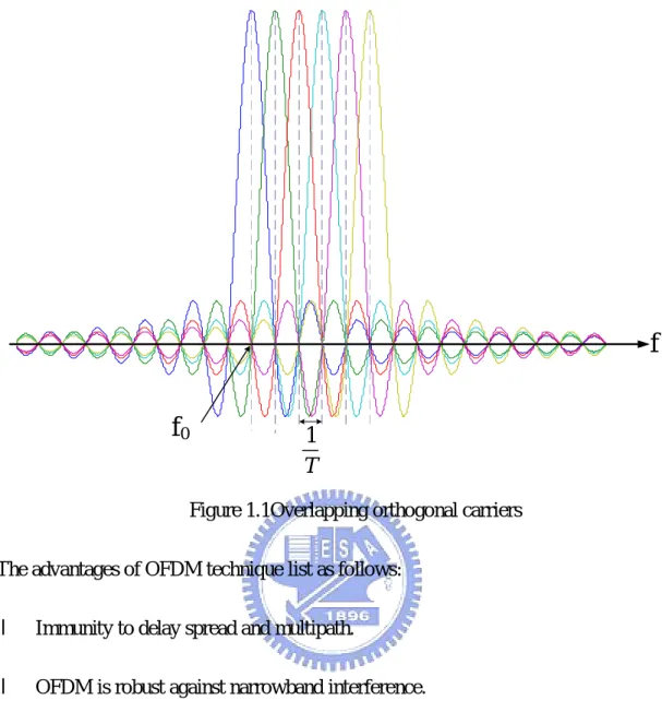
The OFDM carriers exhibit orthogonality on a symbol interval if they are spaced in
frequency exactly at the reciprocal of the symbol interval, which can be accomplished
by utilizing the discrete Fourier transform (DFT). In eq.(1.1)[4] is a OFDM signal
described by mathematical equation, where with N subcarriers and symbol duration is
T, and notice that s(n) is the inverse Fourier Transform of the xi(n). In figure 1.1, it
illustrates spectra of eq. (1.0); the spectrum of the individual carriers mutually overlap
and the interference of adjacent channels is all zero.[4]
1 ( ) ( ) exp(2 ), for 0 ; 0 N A s n x n π f n n N i N − =
∑
≤ ≤ ≤ ≤1
T
f
f
0Figure 1.1Overlapping orthogonal carriers
The advantages of OFDM technique list as follows: l Immunity to delay spread and multipath.
l OFDM is robust against narrowband interference. l Simple equalization.
l Efficient bandwidth usage by overlapping carriers. The disadvantages of OFDM technique are as follows:
l OFDM system is sensitive to carrier frequency offset and phase noise. l OFDM system has relatively large peak to average power ratio.
1.4. Design and Implementation Issues
In UWB system, the high throughput reaching 480Mb/s is the major issue in
hardware design. The ACS block has iterated operation, therefore we can’t speed this
block by pipeline technique. Here, we proposed a arithmetic compare and select (CS)
circuit for speeding the critical path, and we discusses it in chapter 3.
The secondary issue is the trade off between performance and hardware
complexity. The soft decision algorithm, and the traceback length of Viterbi decoder
decide the performance. And we discuss the trade off in chapter 4.
1.5. Organization of this thesis.
This thesis is organized as follows: The first chapter describes a briefly introduction
of UWB. In chapter 2, the specification of IEEE 802.15.3a relative to error correction
coding and the system requirements will be presented. In Chapter 3, the reduction of
proposed CS circuit and analysis of add-compare-select (ACS) will be described.
Chapter 4 describes the design of the Viterbi decoder, including quantization
scheme ,de-puncture and Viterbi decoder, respectively. And it also shows the
simulation result. Chapter 5 shows the achievement of IPQ and FPGA porting. Finally,
Chapter 2
Viterbi Decoder for Ultra-Wideband
2.1 Design Requirements of Viterbi Codec for UWB
The frame format of IEEE 802.15.3a WLAN standard has preamble, header,
payload, and inserted data. The header is always sent at an information data rate of
53.3 Mb/s, and the remainder of the frame is sent at the desired information data rate
of 53.3, 55, 80, 106.7, 110, 160, 200, 320, 400 or 480 Mb/s [1]. The information is
encoded by scrambler, convolution encoder and interleaver. Besides, the different
data rate varies with different puncture scheme.
2.1.1 Scrambler
The frame synchronous scrambler uses the generator polynomial S(x) as follows,
and is illustrated in Fig 2.1:
14 15
( ) 1
In the receiver, we can use the same scrambler structure to descramble the received
data.
Figure 2.1: Scrambler
2.1.2 Convolution Encoder
The convolution encoder of transmitter provide coding rate r=1/3 and constraint
length K=7. The generator polynomials of GA(D), GB(D) and GC(D) as follows are
illustrated in Fig 2.2. Besides general coding rate above, other rates are derived from “puncturing” methodology. [1][7]. GA(D)=1+D2+D3+D5+D6 (2.2) GB(D)=1+D+D4+D5 (2.3) GC(D)=1+D+D2+D3+D4+D6 (2.4) D D D D D D Input Data Output Data A Output Data B Output Data C
2.1.3 Puncture
Puncturing is a procedure for stealing some of the encoded bits in the transmitter.
The coding rate varies with puncture scheme by stealing different transmitted bits.
Figure 2.3 depicts the puncture procedure. De-puncture scheme is inserting a dummy “zero” metric instead of the deleting bit on the decoding side [7] [9]. By combining time spreading and conjugate symmetric input to IFFT and different coding rates,
IEEE 802.15.3a supports ten different data rates.
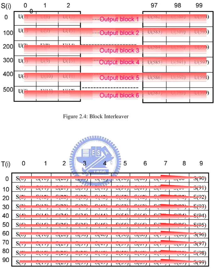
2.1.4 Interleaving
Bit interleaving provides robustness against burst errors. The bit interleaving
operation is performed in two stages: symbol interleaving followed by tone
interleaving. The symbol interleaver permutes the bits across OFDM symbols to
exploit frequency diversity across the sub-bands, while the tone interleaver permutes
the bits across the data tones within an OFDM symbol to exploit frequency diversity
across tones and provide robustness against narrow-band interferers [1].
The input-output relationship of the first permutation shall be given by:
(
)
+ = CBPS CBPS N i N i U i S( ) Floor 6Mod , (2.5)The function floor (.) denotes the largest integer not exceeding the parameter, and
the function Mod(i,NCBPS) is the remainder of NCBPS where NCBPS is the number of
coded bits per OFDM symbol. Figure 2.4 illustrates the permutation of block
interleaver. The input-output relationship of the second permutation is given by:
(
)
+ = Tint T N i N i S i T( ) Floor 10Mod , int (2.6)The value NTint is NCBPS/10 in equation (2.6). Figure 2.5 illustrates the permutation
Figure 2.4: Block Interleaver
2.2 Viterbi Decoder Algorithm
Viterbi Decoder is a maximum likelihood decoder. It finds the closest coded
sequence to the received sequence by processing the sequences on an information
bit-by-bit (branch of the trellis) basis. Generally, Viterbi decoder has four major
decoding steps: branch metric computation, Add-Compare-Select (ACS), path
memory update, and decode symbols. The example is given as Fig 2.6. The trellis
(2,1,2) is shown in Fig 2.6(a) and each state has two connected path. In Fig 2.6(b), the
received data “11” is shown in Fig 2.6(b) and the branch metric is calculated by
comparing with the referenced metric. Each state at t1 selects the minimum path
metric and the information of survivor path is plotted with arrowheads. Fig 2.6(c) and
Fig 2.6(d) continue the operations of add-compare-select at t2 and t3. After all the
information of survivor path is found, the operation of traceback starts at the
minimum path metric. In Fig 2.6(e), the minimum state at t3 is state zero and the
traceback starts at this state. Then, the survivor path is {S0t3, S2t2, S1t1, S0t0} and the
survivor path is plot with thick arrowheads. With decoding scheme, the upper path is
decoded as zero and the lower path is decoded with one. Hence, the received
Received Data 0 2 0 00 11 11 00 01 10 01 10 11 0 0 2 0 1 4 1 1 11 0 00 2 1 1 0 2 0 2 4 1 1 1 2 2 2 11 0 00 2 1 1 11 2 0 0 2 1 1 1 1 0 2 0 2 4 1 1 1 2 2 2 (a) (b) (c) (e) (d) t0 t1 t2 t3 t0 t1 t2 t3 t0 t1 t2 t3 t0 t1 t2 t3 0 2 1 1 1 1 1 1 1 1 1 1 1 1
Figure 2.6: Example for Viterbi Algorithm
In this example above, the received sequence is hard-decision shown in Fig 2.7. The
other case is soft-decision shown in Fig. 2.8.
The soft decision quantizes the sequence from channel and increases the error
correcting capability. Figure 2.8 illustrates the soft -decision quantization. The
transmitted sequence is transmitted in “0” and “1” and the input sequence added with
channel ranges between -∞ and ∞. The positive value is strong one when it is bigger. On the contrary, the negative value is strong zero when it is bigger.
Figure 2.8: Soft Decision
Figure 2.9(a) depicts the radix-2 trellis diagram for the convolution encoder in
802.15.3a standard. It can be transformed into radix-4 trellis diagram shown as Fig.
2.9(b). The high-radix Viterbi Decoder increases the throughput byprocessing two
stages of the constituent radix-2 trellis per iteration [10]. Furthermore, we combine
two radix-4 trace-back iterations into a single radix-16 iteration for the throughput of
We compute the branch metric by the specified trellis and complete the operation
of ACS. Then, the survivor paths can be updated to the memory. After the memory is
filled with the survivor information, the received sequences find its likelihood
decoding path by trace-back method shown as Fig. 2.10 [9].
Chapter 3
ACS module with Arithmetic CS unit
3.1 Deduction of Arithmetic CS unit
Function of compare and select is to find the maximum or minimum value of the
input values. Let the input data as V={v1,v2,v3…… vm } where m is the number of
input data and E={{v1,v2},{v1,v3}……{vi,vj}} where i≠j is a set of two-element
subsets of V. The members in V are called vertices and the members in E are called
edges in graph theory [5]. Generally the maximum value by this method is depicted
below.
2
1 { 1, 2... m} {max{ , }, max{ , }..., max{ ,1 2 1 3 i j}} ,{ , } {0,1, 2... }
M = m m m = v v v v v v i≠ j i j ∈ m
4
2 2 2
2 { 1, 2... m} {max{ 1, 2}, max{ 1, 3}..., max{ i', j'}} ,{ , } {0,1, 2... }
M = m m m = m m m m m m i≠ j i j ∈ m
M
log2 2 2
2
log 1 log 1
log
{
max} {max{
1,
2}}
m m m
m
M
=
m
=
m
−m
− (3.1)the subsets max{mkj−1,mlj−1} where k≠l and the number of the maximum value in V.
We can find that the maximum value of the compared data {v1,v2,v3…… vm } can be
defined as log m times of input and selecting in equation (3.1). 2
We define an ordered pair (vi ,vj) where i≠j and it means vi is greater than vj.
For each member of E we define an ordered pair, and we let R be the set of all such
ordered pairs, and R is indicated in equation 3.2.
1 2 3 m 1 2 1 3 i j
2
R={r ,r ,r ... ,r }={(v ,v ),(v ,v )...(v ,v )} where i≠ j (3.2) In this deduction of the proposed method, we list the combinations of elements and
find the maximum value in different combinations. Finally, we can conclude a logical
equation by Boolean.
For example, we give a V with four elements and V= {v1, v2, v3, v4}. Therefore, it
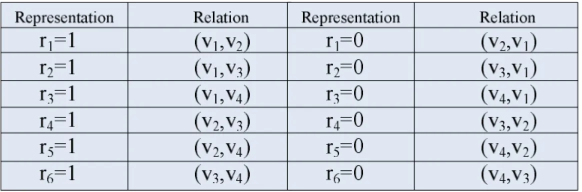
has C24 =6 edges and the edges E={{v1,v2},{v1,v3},{v1,v4},{v1,v2},{v1,v3}},{v1,v4}}
Table 3.1: Relations Definition
In table 3.1 above, we use relations of R where R={r1,r2,r3,r4,r5,r6} to represent the
ordered pairs. When v1 is greater than v2, r1 is equal to zero and v2 is greater than v1
when r1 is equal to one. Therefore we have total 26 kinds of the vector R={r1, r2……,
r6}.
In this deduction of the proposed method, we have two conditions. One is the
maximum value existing, and the other is not.
For example, the conditions are R={r1,r2,r3,r4,r5,r6}={1,1,1,1,1,1} in Fig 3.2. We
can find that all of the arrowheads come from v1. It means v1 is greater than v2 and v3
Figure 3.2: Directed Graph with Maximum Value
The second condition can be illustrated with the directed graph in Fig 3.3, and the
relation is R={r1,r2,r3,r4,r5,r6}={1,1,0,1,1,1}. We infer that in case of the maximum
value being not existing, it forms non radiated vertices. Furthermore, there is a
clockwise loop in {v1, v2, v3}. The vertices in loops will be an unlogical case with
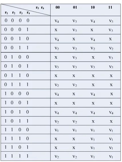
After we analyzed all the 26 conditions, we can list a table as follows. The symbols
of vi corresponds to the 6-bit R is exactly the maximum value among {v1, v2, v3, v4}
and symbol ‘x’ denotes that there is no maximum value can be identified.
Table 3.2: All relations with four input data
We can directly select the maximum value with the known relations from r1 to r6
by using table 3.2.
Finally we can use Boolean reduction on the logical information in table 3.3 and
we can get the result for selecting the maximum value by knowing r1 to r6. 2 4 6 1 2 4 2 3 1 3 4 1 3 4 5 [0] SEL = r r r +r r r +r r +r r r +r r r r (3.3) 2 4 1 3
[1]
SEL
=
r r
+
r r
(3.4)The maximum value is v4 when SEL[0] and SEL[1] are equal to zeros, and the
maximum value is v3 when SEL[0] is equal to one and SEL[1] are equal to zero. The
maximum value is v2 when SEL[0] is equal to zero and SEL[1] are equal to one, and
so on. If we want to change the order, we just exchange the orders of the input data.
3.2 Arithmetic CS Circuit Analysis
We apply the proposed arithmetic CS circuit to Viterbi decoder. In Viterbi
decoder we can not use pipeline technique to speed up the critical block because of
iterated operations. Timing requirement is the main problem of high throughput of
480 Mb/s specified for Ultra-Wideband standard. Hence increasing the throughput or
reducing the delay of critical path will be the key issue of the design.
Firstly, we compare the path delay of CS circuit compared with traditional
comparator. For example, with the number of input data be four and the resolution is
seven. The path delay simulation is done with design compiler (synopsys) and use
UMC 0.18 library for timing analysis.
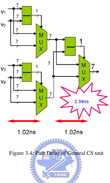
Figure 3.4 shows the traditional comparator. It has three adders and three
Figure 3.4: Path Delay of General CS unit
Figure 3.5 shows the architecture of proposed CS unit. The critical path goes
through one adder and one multiplexer and one combinational block with fixed path
delay. As the input resolution increases the path delay of adder and multiplexer
increase, but the combinational block still has the fixed path delay. Therefore, the
benefits to the path delay in the proposed CS unit increases as the circuit resolution
0.45ns
1 1 1 1 1 7 7 7 7 7 7 7 7 7 7 1 7 70.66ns
M U X 7w
7x
7y
7z
70.37ns
21.48ns
1.48ns
v
1v
2v
1v
3v
1v
4v
2v
3v
2v
4v
3v
42 4 6 8 10 12 14 16 18 20 0.8 1 1.2 1.4 1.6 1.8 2 2.2 2.4 2.6 2.8
Comparison of Path Delay
Resolution (bits) P a th D e la y ( n s ) proposed traditional
Figure 3.6: Comparison of Path Delay between the proposed CS and traditional CS
Simultaneously, we analyze the drawback of the input architecture. The complexity
of the proposed CS circuit increases as the number of compared data increases. The
numbers of adders increase with C2n where n is the resolution bits and table 4 shows
the complexity.
Table 3.4: Complexity of CS unit
Number of input Data 2 4 8 16
Tradition 1 adder 1 mux 3 adders 3 2-to-1muxs 7 adders 7 2-to-1muxs 15 adders 15 2-to-1muxs Arithmetic 1 adder 1 mux 6 adders 1 4-to-1muxs 28 adders 1 8-1muxs 120 adders 1 16-to-1muxs
comparing with higher input architecture. The optimized architecture is applied to the
radix-4 Viterbi codec design and the speed issue is the first consideration.
Furthermore, we analyze the speed, area and power with the arithmetic CS and
general CS. The comparison of gate counts is listed in Fig. 3.7. This trend of
arithmetic CS becomes bigger than general CS because the gate count of adders
increases as the resolution increased and the number of arithmetic CS has three more
than general CS. 2 4 6 8 10 12 14 16 18 20 0 200 400 600 800 1000 1200 1400 1600 Comparison of Area Resolution (bits) G a te C o u n ts proposed traditional
Figure 3.7: Comparison of Area between the proposed CS and the traditional CS
Figure 3.8 illustrates the comparison between the arithmetic CS and the traditional
2 4 6 8 10 12 14 16 18 20 0 2 4 6 8 10 12 14 16 Power Resolution p o w e r proposed traditional
Figure 3.8: Comparison of Power between the proposed CS and the traditional CS
Figure 3.9 illustrated the ratio of figure of merit defined by 12
AT which A is area
and T is the path delay. All the area and timing analysis is run by SYNOPSYS design
compile with UMC.18μm library. The curve below depicts the proposed design is
roughly 1.8 times better than the general design. Besides, the FoM goes down in
2 4 6 8 10 12 14 16 18 20 0.5 0.55 0.6 0.65 0.7 0.75 0.8 0.85 0.9 0.95 1 (A2T)traditional/(A2T)porposed Metric (t ra d it io n a lly N F O M ) / (p ro p o s e d N F O M )
Figure 3.9: Ratio of Figure of merit defined by
2 2 trad proposed AT AT
3.3 ACS module with Arithmetic CS Circuit
Viterbi decoder’s critical path is in Add Compare Select (ACS) block. The timing
limitation comes from feed-back loop. It causes a limit of pipelining data process.
Therefore, how to speed up the add-compare-select block is what we will discuss.[2]
The basic function block of ACS block is called the radix-2 ACS unit. We take the trellis diagram of four states as an example in Fig 3.10.
Γ
t−1 s, 0 is the previoussurvival metric, and
λ
t,s0−>s0 is the branch metric from state 0 to state 0.Γ
t,s0 isthe current metric of the ACS unit.
1, 0 t−s Γ 1, 0 t−s Γ 1, 0 0 t s s λ− −> 1, 1 0 t s s λ− −> 2 , 0 t− s Γ 2 , 0 t− s Γ 1, 0 0 t s s λ− −> 1, 1 0 t s s λ− −> 1, 0 t−s Γ
Figure 3.10: Radix-2 ACS trellis diagram and its function unit
The main consideration of ACS architecture design is the trade off between the
decoder throughput and the number of ACS stage. Several kinds of the ACS
architecture are proposed to achieve the different applications. For low throughput
applications, we can use serial architecture completing the same decoding operations
high radix ACS concept is to decode two or more symbols each time.
Figure 3.11 depicts the conversion from two-stage radix-2 ACS unit to one-stage
radix-4 ACS unit. The radix-4 architecture completes two-stage ACS operations
instead of one-stage ACS operation.
1, 0 t− s Γ 1, 0 t− s Γ 1, 0 t− s Γ 1, 0 t− s Γ , 0 0 t s s λ −> , 1 0 t s s λ −> , 2 1 t s s λ −> , 3 1 t s s λ −> 1, 0 0 t s s λ+ −> 1, 1 0 t s s λ+ −> , 0 0 1, 0 0 t s s t s s λ −> +λ+ −> , 0 0 1, 0 0 t s s t s s λ −> +λ+ −> , 0 0 1, 0 0 t s s t s s λ −> +λ+ −> , 0 0 1, 0 0 t s s t s s λ −> +λ+ −>
Figure 3.11: The Conversion from radix-2 to radix-4
Table 3.5 illustrates the complexity with different number of radix. We select
radix-4 as the basic ACS unit because of some improved techniques and acceptable
cost.
Table 3.5: Complexity of ACS unit
General comparator Arithmetic CS
Radix Complexity
Add operations for branch metric
Comparator operations
Add operations for branch metric
Comparator operations 2 2 1 2 1 4 8 3 8 6 8 24 7 24 28 16 64 15 64 120
In radix-4 ACS unit, we can move the operations of λt−1+λt to the block of
branch metric. Therefore, ACS block reduces the path delay of one adder in the
critical path and doubles the throughput by high radix architecture.
Figure 3.12 illustrates the conversion from the radix-4 ACS unit with two adders
to the radix-4 ACS unit with one adder in the critical path.
1, 0 0 t s s λ− −> λt s, 0−>s0 1, 1 0 t s s λ− −> λt s, 0−>s0 1, 2 1 t s s λ− −> λt s, 1−>s0 1, 3 1 t s s λ− −> λt s, 1−>s0 2, 0 t−s Γ 2, 0 t−s Γ 2, 0 t−s Γ 2, 0 t−s Γ 2, 0 t−s Γ 2, 0 t−s Γ 2, 0 t−s Γ 2, 0 t−s Γ 1, 0 0 , 0 0 t s s t s s λ− −> +λ −> 1, 1 0 , 0 0 t s s t s s λ− −> +λ −> 1, 2 1 , 1 0 t s s t s s λ− −> +λ −> 1, 3 1 , 1 0 t s s t s s λ− −> +λ −>
Figure 3.12: The Conversion from the architecture with eight adders
to the architecture with four adders
Furthermore, we additionally add the Arithmetic CS circuit to the radix-4 ACS unit
and the modified radix-4 ACS is illustrated in Fig. 3.13. In this step, the costs only
come from the property of the proposed CS unit.
Finally, we reduce four times of clock rate for implementation. With consideration
of the trade off between throughput and complexity, we adopt two-stage radix-4 ACS
illustrated in Fig 3.14. 2, 0 t− s Γ 2, 0 t− s Γ 2, 0 t− s Γ 2, 0 t− s Γ 1, 0 0 , 0 0 t s s t s s λ− −> +λ −> 1, 1 0 , 0 0 t s s t s s λ− −> +λ −> 1, 2 1 , 1 0 t s s t s s λ− −> +λ −> 1, 3 1 , 1 0 t s s t s s λ− −> +λ −>
Figure 3.14: Conversion from four-stage radix-2 trellis to two-stage radix-4 x radix-4 trellis
S0 S1 S2 S3 S4 S5 S6 S7 S0 S1 S2 S3 S4 S5 S6 S7
Two-Stage Radix-4 x Radix-4 trellis
S0 S1 S2 S3 S4 S5 S6 S7
Chapter 4
Architecture of Viterbi Decoder
By using the ACS scheme as described in chapter 3, we will discuss the
implementation of outer receiver. Figure 4.1 depicts the function blocks of the
processed Viterbi decoder. The implementation result, including core size, pin
assignment, and timing will be analyzed in this chapter.
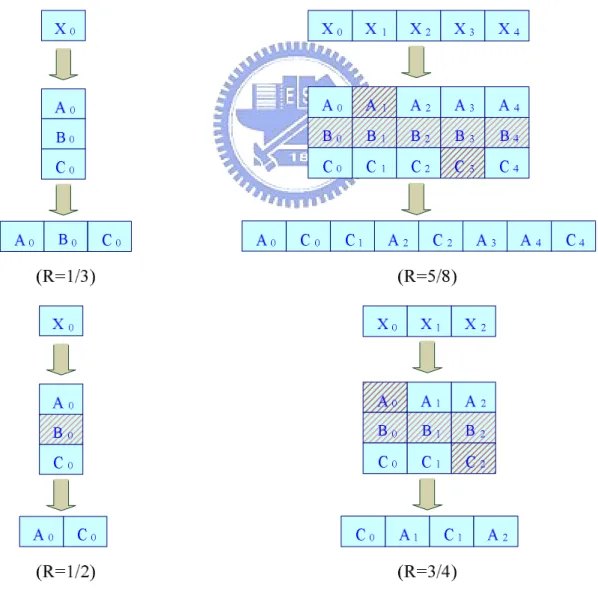
4.1 Depuncture Module
In Viterbi decoding, the stolen bits are not sent in their position of the puncture
scheme. The stolen bits are taken as dummy bits in depuncture task. In the design of
depuncture module, we combine it with branch metric computation (BMC) module.
The following sections in this chapter will discuss the decoding mechanism of each
modulation type, respectively. Notice although we use (3, 1, 3) convolution code to
depict these patterns, the same situations also apply for (3, 1, 7) convolution code in
the following discussions. As depicted in Fig. 4.2, Fig 4.3, Fig 4.4 and Fig 4.5, the
patterns of four kinds of coding rate, 1/3 ,11/32 ,1/2 ,3/4 & 5/8 are shown,
respectively. S0 S1 S2 S3 S0 S1 S2 S3 000 10 1 111 011 010 110 10 0 001 S0 S1 S2 S3 000 10 1 111 011 010 110 10 0 001 S0 S1 S2 S3 000 10 1 111 011 010 110 10 0 001 S0 S1 S2 S3 000 10 1 111 011 010 110 10 0 001 S0 S1 S2 S3 000 10 1 111 011 010 110 10 0 001
1X1 0X1 0X0 1X0 1X1 0X1 0X0 1X0 1X1 0X1 0X0 1X0 1X1 0X1 0X0 1X0 1X1 0X1 0X0 1X0
Figure 4.3: The pattern of coding rate 1/2
XX 1 X X1 X X1 XX 0 XX 0 X X 0 1X 1 1X 1 0X 1 0X0 1X0 1X 0 1X X 1X X 0X X 0XX 1XX 1X X XX 1 X X1 X X1 XX 0 XX 0 X X 0 1X 1 1X 1 0X 1 0X0 1X0 1X 0 1X X 1X X 0X X 0XX 1XX 1X X
Figure 4.4: The pattern of coding rate 3/4
S0 S1 S2 S3 S0 S1 S2 S3 XX0 XX 1 X X 1 X X 1 XX 0 XX 0 X X 0 XX1 S0 S1 S2 S3 0X0 1X 1 1X 1 0X 1 0X0 1X0 1X 0 0X1 S0 S1 S2 S3 0XX 1X X 1X X 0X X 0XX 1XX 1X X 0XX S0 S1 S2 S3 0X0 1X 1 1X 1 0X 1 0X0 1X0 1X 0 0X1 S0 S1 S2 S3 0X0 1X 1 1X 1 0X 1 0X0 1X0 1X 0 0X1
4.2 Viterbi Decoder Module
Generally, the parameters of Viterbi decoder contain the resolution bits of soft
decision and traceback length. Number of resolution brings the trade off between
performance and complexity. Besides, the resolution bits of soft decision influences
the path delay and the complexity of ACS module. Fig 4.6 depicts the quantization of
soft four. For the requirement of Ultra-Wideband standard, the coding gain needs
above 5dB. For the property of Viterbi decoder, the performance approximates the
ideal case with 4 bits resolution. But the performance of three bits resolution is similar
to the performance of 4 bits resolution.
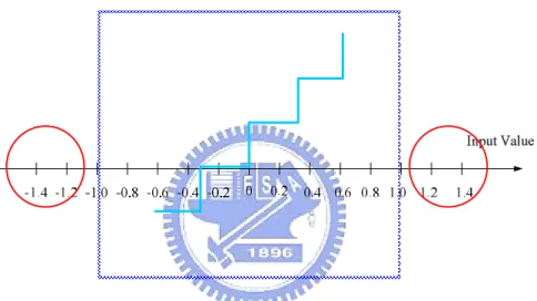
-2 -1.5 -1 -0.5 0 0.5 1 1.5 2 0 1 2 3 Input value QPSK Demapping I -2 -1.5 -1 -0.5 0 0.5 1 1.5 2 0 1 2 3 Input value QPSK Demapping Q
Hence soft-decision eight illustrated in Fig. 4.7 is selected for satisfying the
requirement of UWB specification by our simulation illustrated in Fig 4.8.
-2 -1.5 -1 -0.5 0 0.5 1 1.5 2 0 2 4 6 8 Input value D em ap pi ng QPSK Demapping -2 -1.5 -1 -0.5 0 0.5 1 1.5 2 0 2 4 6 8 Input value D em ap pi ng QPSK Demapping I Q
Figure 4.7: Quantization of soft decision 8
1.5 2 2.5 3 3.5 4 4.5 5 10-6 10-5 10-4 10-3 10-2 10-1 Eb/N0 (dB)
Hard decision and soft decision
hard soft4 soft8 soft16
4.2.1 BMC Module
The caculation of branch metric in Euclidean distance is listed in equation (4.1).
The values of XI , YI and ZI are the received metric and the values of XI ,YI and ZI are
the reference metric from the derived trellis.
2 2 2
, , ,
( I r i) ( I r i) ( I r i)
BM = X − X + Y −Y + Z −Z (4.1)
The square value is not desirable for hardware implementation. Though, the metric of
correlation derived form equation (4.1) is used in the calculation of branch metric [7].
The modified branch metric calculation equation is represented as:
, , ,
'
X i Y i Z iBM
=
M
+
M
+
M
(4.2)The values of MX,i, MY,i and MZ,i are the modified metric obtained from table 4.1.
Table 4.1 shows the conversion of
X
I under bit 1 and bit 0, respectively. The metricis the received value when the referenced bit is one. On the contrary, the metric is
calculated by subtracting 7 from the received value.
For example, the decoder receives (0,3,7) symbol and the referenced bits are (0,1,0).
Table 4.1: The mapping table of metrics by the correlation algorithm [7]
Because of radix-4 ACS architecture, the BM needs the summation of six received
metric. With soft-decision 8, the maximum value of BM is 42 and it needs six bits and
it influences the resolution of ACS. The BM is limited in five bits by subtracting those
values exceeding 31. Fig 4.9 illustrates the offset for subtraction. Figure 4.10
illustrates the architecture of radix-4 branch metric unit.
Figure 4.10: The radix-4 branch metric element
4.2.2 ACS Module
4.2.2.1 Implementation Issues
Depending on chapter 3 we have described, the two-stage radix-4 ACS
architecture used in the literature. Table 4.2 lists the complexity and design respects of
different ACS units. With consideration of backend margin, we use two-stage radix-4
with arithmetic CS.
Table 4.2: Analysis of ACS architecture
Modified Radix-4 1194.5 16.39 2.94 (target=4.16ns) 8 adders,6 comparators 240 Mhz 480Mb/s Radix-4 with arithmetic CS 782 10.3 2.75 ns(target=4.16ns) 4 adders,3 comparators 240 Mhz 480Mb/s Modified Radix-4 1066.1 15.19 3.48 (target=4.16ns) 8 adders,3 comparators 240 Mhz 480Mb/s Radix-4 362.5 4.29 1.83 ns (target=2.08ns) 2 adders, 1 comparator 480 Mhz 480Mb/s Radix-2 ACS unit Area(gate counts) ACS unit Power
(mW) ACS unit Min.
Delay(ns) Hardware Complexity Min. required clock(Mhz) Throughput Modified Radix-4 1194.5 16.39 2.94 (target=4.16ns) 8 adders,6 comparators 240 Mhz 480Mb/s Radix-4 with arithmetic CS 782 10.3 2.75 ns(target=4.16ns) 4 adders,3 comparators 240 Mhz 480Mb/s Modified Radix-4 1066.1 15.19 3.48 (target=4.16ns) 8 adders,3 comparators 240 Mhz 480Mb/s Radix-4 362.5 4.29 1.83 ns (target=2.08ns) 2 adders, 1 comparator 480 Mhz 480Mb/s Radix-2 ACS unit Area(gate counts) ACS unit Power
(mW) ACS unit Min.
Delay(ns) Hardware Complexity Min. required clock(Mhz) Throughput
.2.2 ACS Overflow Prevention
The operation of ACS module is recursive and its word-length is finite. Therefore,
if we do not prevent the overflow from appearing, the results of survivors will go
wrong.
We use the common method. First, we set the overflow threshold based on
resolution 7 bits. The path metrics are subtracted from a truncated threshold at each
state when the overflow happens. And those path metrics below the truncated
threshold are set zero. When the path goes through 4-stage trellis diagram, the new
path metrics will replace the original. Therefore, the overflow problem would never
happen [12] [13] .
For example, the path metrics are set as (70, 40, 33, 10) in Fig.4.11. With the
overflow path metric appeared, the new path metrics are (38, 8, 1 ,0) after overflow
prevention.
(b) Path metrics after overflow prevention
Figure 4.12 depicts the architecture of overflow prevention unit.
overflow M[6:0]
=
M[6:5] 2'd0 0 1 5'd0 7 9 1 2 0 1 7 7 1 Survivor metric 7 Survivor metric -2'd1 M[6:5] M[4:0] M[6:0]Figure 4.12: Overflow prevention element
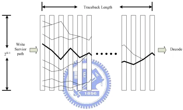
4.2.3 Traceback Module
In the literature, the traceback algorithm is adopted for decoding mechanism. We
input path will be asserted and one of the output survivor path will be passed..
Figure 4.13: The radix-4 traceback element
The traceback architecture is a combinational circuit shown in Fig. 4.13, including
48x40 traceback elements. The starting state starts at zero state in this design.
The decoding mechanism is according to the trellis structure. Table 4.3 where i
ranges from 0 to 15 depicts the decoding table for our trellis structure. In this table,
the traceback path goes into the decoded states. The decoded bits can be decoded by
its survivor states. Figure 4.14 illustrates the traceback architecture.
Figure 4.14: The traceback architecture
4.2.4 Discussion between different Traceback Length
For the demand of real-time decoding mechanism, the information of survivors
must be transmitted to the traceback architecture parallel from ACS block. Therefore,
registers are used as storage in the high speed design.
Generally, the traceback length is five times more than the constraint length [9].
Consideration of implementation, the path delay in the combinational circuit can not
of Fig. 4.15. Besides, the path delay is still too long to be finished in a clock cycle.
Therefore, the property of path merge can be used for multi-cycle design [14].
2 2.5 3 3.5 4 4.5 5 5.5 10-7 10-6 10-5 10-4 10-3 10-2 10-1 Eb/N0(dB) B E R
Comparision of merging length about radix-4
28 32 36 40 50 60
Figure 4.15 Performance between different traceback Length
In the design, the path delay of the tracebacck module is roughly 13ns. Which can
not be completed during one clock cycle and it takes two clock cycle for completing
the operation of trackback, and the decoding length is eight. This design also
decreases the power consumption because of the reduction of registers switches. The
total registers of the traceback module are 56x64 bits, and the extra 8x64 bits are for
Chapter 5
Implementation and Verification
5.1 Introduction
In this chapter we discuss the design flow, verification plan, IP qualification and
co-simulation for the proposed design. In this study, behavior model is built by C
which is bit accurate and a MATLAB model for system co-simulation with RF. The
design flow is illustrated in Fig. 5.1, and this is a kind of waterfall models which
works well up to 100k gate count design. It is a serial flow from specification survey
to post layout and there integrate a verification flow to verify the design [15]. In this
design flow, the RTL module is verified by accurate C model and the system
co-simulates with MATLAB model. Why do we use two behavior models? The reason
is that C program has much higher processing speed than MATLAB and for MAC
link. For example, the simulation time by MATLAB is too long when the amount of
simulation is up to 106and not to mention applying more information. Besides, with
the behavior model the baseband and RF co-simulation platform can be built in
After RTL code is development and verified, there are two ways for implementing
design, one is ASIC, and the other is FPGA prototyping. FPGA prototyping is for
verifying hardware design in general, because FPGA can simulate the work in real
world and some situations which we don’t concern may appear. If we want to produce
ASIC or IP, we will go through synthesis and Place & Route. First, we synthesis the
design to gate-level netlist by reasonable design constrains. After checking the timing,
area and power, we will run Place & Route. After timing, area, power and design rule
5.2 System co-simulation
Figure 5.2 Design & Verification flow
Our system is illustrated in Fig. 5.2. The platform by MATLAB is based on
802.15.3a standard. The pattern is transmitted in ten rates with the varieties of
puncture scheme, conjugate and spreading. Figure 5.3 depicts the pack error rate at
480Mb/.
In system co-simulation, we firstly know that the information of RF simulation is
viewed as timed sequence. Hence, the sequences calculated by MATLAB should be
packed and transformed into timed sequence. Then, RF team can check their
parameter settings and performance, such as TX EVM, TX power spectrum, RX
6 8 10 12 14 16 18 20 22
10-3
10-2
10-1
100
Packet error rate at 480 Mb/s
SNR P E R awgn CM1 CM2
Figure 5.3 Pack error rate at 480Mb/s
RF TX
RF RX
BB_TX
5.3RTL Design and soft IP Qualification
Figure 5.5: The proposed Viterbi Decoder architecture
The synthesizable RTL is desired according to the architecture discussed in chapter 3
and the architecture is illustrated in Fig 5.5. In this study, we also discuss the soft IP
qualification (IPQ). IPQ has its defined coding style [16]. Table 5.1 and Fig 5.6 depict
the number of coding rules fitting IPQ in our design. In this table, two warnings come
from the architecture of feed-back circuit because of overflow prevention and the
others are header warnings.
Table 5.1 Number of coding rules fits IPQ
25 2132 Warnings M1 & M2 0 1076 Errors ERROR After Modification Before Modification 25 2132 Warnings M1 & M2 0 1076 Errors ERROR After Modification Before Modification
Figure 5.6 Design & Verification flow
The IPQ needs reasonable test patterns for function verification. The code coverage
means that the percentage of the verified design is checked in different verifying
methodology. The code coverage of statement, condition and toggle coverage are
almost up to 100% in our design. The results are illustrated in Fig 5.7, Fig 5.8 and Fig
5.9. And we list the met soft IP qualification in table 5.2.
Figure 5.9 Toggle coverage
5.4 Function Verification.
Functional verification and debugging usually cost about double time more than
develop a RTL code. First, a bit accurate C model based on the decided architecture is
built. The BER of C program simulation is compared with ideal Viterbi decoder and
satisfied with the requirement of Ultra-Wideband specification. Second, we decide the
interface and write the testbed for RTL simulation. Figure 5.10 illustrates the
verification plan. The patterns are added with noise and decoded with C model. The
testbed is fed with the pattern generated form C program. After finishing the RTL
simulation, the BER of C model and BER of RTL code are compared for analyzing
the consistency. The gate-level simulation is depicted in Fig 5.11.
Figure 5.11 Gate level simulation
5.5 Timing and Area analysis
We use SYNOPSYS design compiler to synthesize the register-level Verilog file
with UMC0.18 slow library. And the parameters of the Viterbi Decoder are: 3-bit soft
decision and traceback-length 40. The gate counts and the critical path delay of each
module is shown in Table 5.3, respectively.
Table 5.3 Synthesis reports for each module
Module Name Gate Count
BMC (depuncture) ACS TB TB_control 21146 83865 18988 38322 Max. Path Delay (ns) 3.72 6.84 13.52 1.59
5.6 FPGA prototyping.
Figure 5.12: The FPGA verification plan
The input pattern is saved in pattern generator and sent to FPGA. Then, we check
the result by waveform or dump the result file for checking. In this study, we build
another synthesizable built-in testbed and test pattern in FPGA. The self-check testbed
has synthesizable verification pattern and self-check circuit for cycle accurate error
checking. The FPGA verification plan is shown in Fig. 12. Figure 13 depicts the
verifying situation.
Table 5.4 Xilinx FPGA synthesis report.
Target Device xcv2000e-bg560-6
Slices 12252
Slices Flip Flops 6419
5.7 Implementation Results
The macro is implemented by cell-based design flow, and fabricated in 0.18
CMOS process. We use SYNOPSYS Design Compiler to synthesize the gate-level
Verilog file. And the parameters of the Viterbi Decoder are: 3-bit soft decision and
traceback-length 40. The pins of Viterbi module are shown in Fig 14.
Figure 5.14: Viterbi Interface
The timing diagram is illustrated in Fig 5.15. Because of two-stage radix-4
architecture, the design uses the quarter clock. The first decoded data is calculated
after sixteen clock cycles when the Viterbi decoder starts decoding. In the first sixteen
clock cycles, the data passes through the blocks of BM and ACS and fills the
Figure 5.15 Timing Diagram
Figure 5.16 BMC Module
Figure 5.18 TB Module
The detail pins assignment of sub modules are depicted in Fig 5.16, Fig. 5.17 and
Fig. 5.18.
Table 5.5: The layout area of the proposed design
The maximum operation frequency is 120MHz and the throughput is 480Mb/s. The
PAR process of layout is applied with SYNOPSYS ASTRO by UMC 0.18μm. The
area of the layout is shown in Table 5.5. Figure 5.19 depicts the macro layout view of
5.8 Performance Analysis
Table 5.6 Comparison of Viterbi Decoder
This design
VLSI design and implementation of high-speed Viterbi decoder
[12]
200Mbps Viterbi Decoder for UWB[2]
Synthesis speed & synthesis library
6.84ns with UMC018 slow library N/A N/A Synthesis gate count 176K 50K 87K Throughput 480Mb/s @120Mhz 200Mb/s @100Mhz 200Mb/s @100Mhz Latency 4+12=16 clock cycle (at quarter clock rate )
N/A N/A
P&R speed 8.13 ns N/A N/A
P&R core area 2037 x 1564.64 um2 3.88 mm2 @.25CMOS N/A
resolution Soft-decision 8 N/A Soft-decision 8
Architecture Two-stage radix-4 Radix-4 Radix-4
Parameters (3,1,7) TB length=40 (2,1,7) TB length=32 (3,1,7) TB length=42
decoder for Ultra-Wideband standard has higher throughput than others listed in this
table. And the latency contain 24 clock cycles from filling traceback module and the
Chapter 6
Conclusions and Future Work
6.1 Conclusions
As the SOC trend becomes popular, the qualification of IP is more important. In
this thesis, we consider the soft IP qualification and process the macro design with
P&R. Besides, we propose a high performance and high throughput Viterbi decoder
for WLAN IEEE 802.15.3a. For soft decision resolution issue, we apply 3-bit soft
decision for demapping design. For traceback-length issue, we employ
traceback-length 40 in Viterbi decoder. For ACS module, we apply many techniques
to improve the critical path such as arithmetic CS and branch metric limitation.
system integration, the module could use different clock source from outer clock.
Hence, it increases the complexity of integration. Therefore, the higher radix
architecture or better P&R techniques could be applied. We can optimize the ACS
module in P&R view. Besides timing issue, the high speed ram based design and
Bibliography
[1] A. Batra, et al., “MultiBand OFDM Physical Layer Proposal for IEEE 802.15
Task Group 3a,” http://www.multibandofdm.org, September 2004.
[2] Sung-Woo Choi and Sang-Sung Choi, “200Mbps Viterbi decoder for UWB,”
ICACT, 2005.
[3] Richard van Nee and Ramjee Parsad, “OFDM Wireless Multimedia
Communications,” Artech House, 2000.
[4] J. Heiskala and J. Terry, “OFDM Wireless LANs: A Theoretical and Practical
Guide,” Sams, 2002.
[5] Fletcher, Hoyle, Patty, “Foudations of Disiscrete Mathematics,” PWS-KENT.
[6] A. K. Yeung, and I.M. Rabaey, “A 210Mb/s Radix-4 Bit-level Pipelined Viterbi
Decoder”, IEEE Int. Solid-State Circuit Conf., pp. 88-90, 1995.
[7] Chia-Hsin Lin “Design and Implementation of 802.11a/g OFDM-Based Outer Receiver”. Thesis, National Chiao Tung University, Taiwan.
[8] Chien-Ching Lin, Chia-Cho Wu, and Chen-Yi Lee, “A Low Power and High
Speed Viterbi Decoder Chip for WLAN Applications” Solid-State Circuits
[10] Black, P.J.; Meng, T.H., “A 140-Mb/s, 32-state, radix-4 Viterbi decoder”, IEEE
JOURNAL OF SOLID-STATE CIRCUITS.
[11] Lin Costello, “Error Control Coding 2/e”, Prentice Hall PEARSON, 2004.
[12] Y. Y. Xin, W. J. Xiang, L. F. Chang and Y. Y. Zheng, “VLSI design and
implementation of high-speed Viterbi decoder”, Communications, Circuits and
Systems and West Sino Expositions, IEEE 2002 International Conference
on, Volume: 1, 29 June-1 July 2002.
[13] A. K. Yeung, and I.M. Rabaey, “A 210Mb/s Radix-4 Bit-level Pipelined Viterbi
Decoder”, IEEE Int. Solid-State Circuit Conf., pp. 88-90, 1995.
[14] Suk-Jin Jung, Myeong-Hwan Lee#, and hyung-Jin Choi, “A New Survivor
Memory Management Method In Viterbi Decoders: Trace-Delete Method and Its
Implementation”, IEEE Int. Global Telecommunications Conf., pp. 3284-3286,
1996.
[15] Ko-Hui Lin “Design of FFT/IFFT module for Ultra Wideband System”. Thesis,
National Chiao Tung University, Taiwan.
[16] IP Qualification 標 準 制 定 聯 盟 ,”IP Qualification Guidelines”
簡 歷
姓名 : 蔡彥凱 性別 : 男 籍貫 : 桃園縣 生日 : 民國七十年六月二十號 地址 :桃園縣中壢市龍岡里龍門街 161 巷 2 號 學歷 : 國立交通大學電子工程研究所碩士班 93/09~95/06 國立成功大學機械工程學系 88/09~93/06 省立武陵高級中學 85/09~88/06論文題目 : Viterbi Decoder Design for Ultra-Wide band System 用於 UWB 設計之 Viterbi 解碼器
![Table 1.2 Timing-related parameters. [1]](https://thumb-ap.123doks.com/thumbv2/9libinfo/8611865.190787/14.892.134.758.320.703/table-timing-related-parameters.webp)