國 立 交 通 大 學
電子工程學系 電子研究所碩士班
碩 士 論 文
氧化鉿電阻式記憶體之操作方法與隨機電
氧化鉿電阻式記憶體之操作方法與隨機電
氧化鉿電阻式記憶體之操作方法與隨機電
氧化鉿電阻式記憶體之操作方法與隨機電
報
報
報
報雜訊研究
雜訊研究
雜訊研究
雜訊研究
Study of Operation Method and Random Telegraph Noise
in HfOx-based RRAM
研 究 生 :王柏偉
指導教授 :汪大暉 博士
陳旻政 博士
氧化鉿電阻式記憶體之操作方法與隨機電
氧化鉿電阻式記憶體之操作方法與隨機電
氧化鉿電阻式記憶體之操作方法與隨機電
氧化鉿電阻式記憶體之操作方法與隨機電
報
報
報
報雜訊研究
雜訊研究
雜訊研究
雜訊研究
Study of Operation Method and Random Telegraph Noise
in HfOx-based RRAM
研 究 生 : 王柏偉 Student : Bo-Wei,Wang
指導教授 : 汪大暉 博士 Advisor : Dr. Tahui Wang
指導教授 : 陳旻政 博士 Advisor : Dr. Min-Cheng Chen
國立交通大學
電子工程學系 電子研究所碩士班
碩士論文
A Thesis
Submitted to Department of Electronics Engineering & Institute of Electronics
College of Electrical and Computer Engineering
National Chiao Tung University
In Partial Fulfillment of the Requirements
For the Degree of Master
In
Electronic Engineering
July 2013
Hsinchu, Taiwan, Republic of China.
i
氧化鉿電阻式記憶體之操作方法與隨機電
報雜訊研究
學生:王柏偉
指導教授:汪大暉 博士
指導教授:陳旻政 博士
國立交通大學 電子工程學系 電子研究所
摘要
本篇論文主要先針對 HfOx-Based RRAM 作 Sweep 與 Pulse 操作下其記憶體特
性之探討,並在最佳化的操作下量測其不同電阻組態並統計分析其 RTN 之累積
密度分佈函數,最終也比較了不同厚度的 HfOx 層造成的 RTN 統計分布的影響。
對於 RRAM 而言,改變其電阻組態的方法有 Sweep 及 Pulse 兩種電性方式,
我們將此兩種方式套用至 RRAM 的 forming 與 Set/Reset 操作中並發現以 Sweep
forming 並以 Pulse Set/Reset 的方法使 RRAM 有最大的阻值變化與操作次數。我
們在將 RRAM 操作於不同阻態的過程中量測了 RTN 造成的電流變化,並依電流
大小作統計分析,發現不同厚度的 HfOx 的 RRAM 在各個阻值態下其 RTN 累積
密度分佈函數皆呈現指數分布,在高阻值態下並呈現兩段式斜率。其中 RTN 大
小之平均值皆隨著電阻阻態增加而增加,但是在較薄的 HfOx 層中其平均值變化
較不明顯。
ii
Study of Operation Method and Random Telegraph
Noise in HfOx-based RRAM
Student: Bo-Wei Wang Advisor: Dr. Tahui Wang
Advisor: Dr. Min-Cheng Chen
Department of Electronics Engineering &
Institute of Electronics
National Chiao Tung University
Abstract.
In this thesis, we find the optimized method of operations of the RRAM with sweep and pulse operations. We measured the RTN amplitude cumulative density function (CDF) in different current orders and compared the influences with different HfOx thickness on the cumulative density functions.
There are two electrical ways to switch the resistance of RRAM: sweep & pulse. We applied these two ways to the forming & Set/Reset operations of RRAM, and we find the sweep forming & pulse Set/Reset operation method has the best characteristics of memory window and endurance. We measured the RTN amplitude CDF in different current orders in both 60Å and 30Å devices, and the CDF follow a exponential distribution in each current order. The CDF of high resistance states (HRS) have two distribution trends. In both 60Å and
iii
30Å devices, the main distributions follow an exponential trend and the average of RTN amplitude increase with the resistance, but the amount of change is less sensitive to the resistance in 30Å devices.
iv
Acknowledgement
本篇論文完成,首先要感謝指導教授汪大暉教授及陳旻政博士。汪大暉教授及陳旻 政博士提供了良好的實驗儀器及研究環境,使我們可以進行許多先進元件的研究。他紮 實且深入的研究訓練,加上嚴謹的研究態度,讓我獲益良多。 再來最需要感謝的就是指導我實驗的鍾岳庭學長。在實驗做不出來的時候,給我明 確的方向,也教了我做實驗的方法與態度。另外還要感謝實驗室的榮標、佑亮、泓達和 定樺學長給予我生活上和學業上的意見,在我剛進實驗室時,幫助我融入這個實驗室。 同屆的子譯、宇恆還有啟偉,感謝他們在我失意的時候,都能在我身邊給予我精神上的 支持。最後還有學弟晉榕、柏誠、宇軒、學妹思嫻和莊 group 的同學們,讓我的研究生 生活,除了嚴肅的學術研究外,還多了許多歡樂。 最後要感謝我的父母、家人,在求學期間給我的鼓勵和支持,有了他們經濟上支持, 無怨無悔的付出與關心,才能讓我完成我的碩士學位。 2013.7
v
Contents
Chinese Abstract
i
English Abstract
ii
Acknowledgement
iv
Contents
v
Figure Captions
vi
Chapter 1
Introduction
1
Chapter 2
Method of Operation and Characteristics
of RRAM
6
2.1
Introduction
6
2.2
Device Details and Measurement setup
6
2.3
Current Compliance for Sweep Forming and
Current Overshoot
7
2.4
Sweep
and
Pulse
Operation
for
Forming/Set/Reset
8
2.4.1
Sweep Forming & Sweep Set/Reset
8
2.4.2
Pulse Forming & Pulse Set/Reset
8
2.4.3
Sweep Forming & Pulse Set/Reset
9
Chapter 3
RTN Main Distribution in HfOx-based
RRAM
18
3.1
Introduction
18
3.2
RTN Distributions in RRAM
18
3.3
RTN Main Distributions with Weibull Analysis
in 60Å and 30Å RRAM
19
Chapter 4
Conclusions
37
vi
Figure Captions
Fig. 1.1 Classification of the resistive switching effects which are considered for non-volatile memory applications [1.5].
p.3
Fig. 1.2 Valence Change Systems [1.5]. p.4
Fig. 1.3 Illustration of the behavior of O2- and Vo during set/reset process [1.9]. p.5 Fig. 2.1 Illustration of the device in this chapter. The top electrode is TiN,
bottom electrode is n+ poly Si, and the HfOx is sandwiched between the electrodes with Height: 60Å Width: 0.6um Length: 0.6um.
p.10
Fig. 2.2 The connection of the instruments. The read voltage is -0.1V in order to avoid the read disturb.
p.11
Fig. 2.3 The current compliance Ic for sweep forming has no effect on the
resistance after the forming process if the Ic is larger than a threshold
current about 80uA.
p.12
Fig. 2.4 (a) Current overshoot induces the result that the reset current is larger than compliance current [2.3].
(b) 1R RRAM device can follow the line of Ireset ≈ Ic with reduced
HfOx [2.4].
p.13
Fig. 2.5 The Ireset ≈ Ic when the compliance current is larger than 80uA. p.14
Fig. 2.6 (a) Sweep set/reset cycles, the hysteresis phenomenon is obvious. (b) The memory window is small and it becomes closed when cycle
times go over 600.
p.15
Fig. 2.7 (a) A reverse operation result due to pulse forming. (b) A normal operation result for pulse forming.
vii
Fig. 2.8 The memory window and endurance of sweep forming& pulse set/reset is better.
p.17
Fig. 3.1 The oxygen vacancies may appear near the conducting filaments as the RTN traps.
p.22
Fig. 3.2 Multi-level RTN is easy to observe in HfOx-based RRAM. p.23
Fig. 3.3 The RTN distributions in different current levels. The distributions split at the region of small amplitude.
p.24
Fig. 3.4 There is no effect on the slope of the main distributions when the tails are removed in different amplitude.
p.25
Fig. 3.5 (a) The RTN main distributions split and follow a straight line in each current level.
(b) The average of RTN amplitude increase with the resistance states.
p.26
Fig. 3.6 (a) The RTN main distributions in 30Å RRAM in each current order seem to be closed.
(b) The average of the RTN amplitude in 30Å RRAM increase lightly with the resistance states.
p.27
Fig. 3.7 The distributions of RTN amplitude in 60Å RRAM follow straight line with slope equals to one in each current level in Weibull plot.
p.28
Fig. 3.8 The distributions of RTN amplitude in 30Å RRAM in Weibull plot. p.29 Fig. 3.9 (a) The distributions rebuild in 60Å RRAM.
(b) Distribution of Current order E-6 rebuild in 30Å RRAM. (c) Distribution of Current order E-7 rebuild in 30Å RRAM. (d) Distribution of Current order E-8 rebuild in 30Å RRAM.
viii Fig. 3.10 (a) The I
I
∆
increase lightly with resistance in 30Å RRAM in comparison with 60Å RRAM.
(b) The values of ∆I are similar in both 60Å and 30Å RRAM.
p.31
Fig. 3.11 (a) For current order E-6,the RTN amplitude distribution with tail removing seems to be very similar to each other for 30Å and 60Å devices.
(b)(c) The RTN amplitude distributions in 60Å devices are more larger than the RTN amplitude distributions in 30Å devices for the current order of E-7 and E-8.
p.32
Fig. 3.12 Read failure is much serious in thick HfOx devices. p.33
Table I Value of k and λ in 60Å RRAM. p.34
Table II Value of k and λ in 30Å RRAM. p.35
1
Chapter I
Introduction
For downscaling flash non-volatile memory, the technology node is approaching the physical and electrical scaling limitation [1.1][1.2][1.3]. In the last few years, the resistance switching random access memory (RRAM) has been raising interest due to their potential for high density, low voltage operation, scalability and low fabrication cost with CMOS process compatibility [1.4]. The RRAM cell is built by a MIM or MIS capacitor-like structure. The materials of the insulating oxide layer and the two electron conductors play important role in the phenomenon of resistance switching (Fig.1.1)[1.5]. An electrical forming operation which is usually required to activate the resistance switching property is distinctive to other kinds of non-volatile memories. For HfOx-based RRAM, the forming process constructs a path usually called conducting filament (CF) which is formed along the grain boundary by the oxygen vacancies [1.6]. The set/reset resistance switching mechanism has been attributed to the formation/rupture of the CF with oxygen vacancies [1.7], and this fluctuation of the CF can be connected to the variance of the energy band diagram (Fig.1.2) [1.5]. For bipolar operating principle in HfOx-based RRAM ( the HfOx-based RRAM can be operated in unipolar method
[1.8]), the oxygen ions O2- can be pulled out from the lattice and accumulated at the electrode according to the polarity of applied voltage during the forming/set process, and the oxygen vacancies Vo would be generated to be defects in the dielectric layer. When the concentration of the Vo is sufficiently high, the transition of resistance from high resistance state (HRS) to low resistance state (LRS) means the success of the forming/set process. For the process of reset, by applying a voltage with opposite polarity to the forming/set, the resistance state will be changed from LRS to HRS when the O2- be attracted by the electric field and move from
2
the electrode to the dielectric layer and recombined with the Vo (Fig.1.3) [1.9].
The operation for resistance switching of RRAM can be classified in two electrical methods, sweep and pulse. In chapter 2, a comparison between the sweep and pulse in processes of forming and set/reset is accomplished without the issue of current overshoot, which may induce the result that reset current is larger than the forming/set compliance current [1.10].
The conducting mechanism in HfOx-based RRAM is trap-assisted-tunneling [1.11] by the oxygen vacancies Vo in the conducting filaments. Nevertheless, the generated Vo may occupy the lattice points which are not in the conducting filaments and play the role of traps for random telegraph noise (RTN) through the blocking mechanism or trap-assisted-tunneling (TAT) mechanism [1.12]. In chapter 3, base on the best method of operation which is found in chapter 2, the distributions of cumulative density function (CDF) for amplitude of random telegraph noise are measured in different thickness of HfOx layers. The RTN distributions demonstrate the blocking mechanism and the TAT mechanism. The dependence of RTN distributions on resistance states and oxide thickness is determined in chapter 3. Finally, the conclusion is accomplished in chapter 4.
3
Fig. 1.1 Classification of the resistive switching effects which are considered for non-volatile memory applications [1.5].
4
5
6
Chapter 2
Method of Operation and Characteristics of RRAM
2.1 Introduction
The HfOx-based RRAM can exhibit the non-polar switching behavior [2.1], namely, the polarity of the applied voltage can be either bipolar or unipolar mode. In this chapter, the sweep and pulse operation methods are applied to the process of forming and set/reset with bipolar mode respectively. The differences between the sweep and pulse operation are the process time and the process voltage. Before the tests of operation methods, the effects of the compliance current for sweep forming are demonstrated. According to the result of experiments, the compliance current for successful sweep forming process has to be bigger than the threshold compliance current which is about 80uA. To identify the influence of current overshoot, the devices are operated in different compliance current to observe the maximum reset current.
2.2 Device Details and Measurement setup
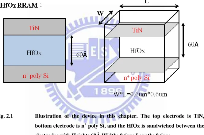
The structure of device we used in this chapter is illustrated in Fig. 2.1. The devices are HfOx-based RRAM with the TiN top electrode and the n+ poly Si bottom electrode, the thickness of the HfOx layer is 60Å, the width is 0.6um and the length is 0.6um. The devices are manufactured by the Nano Device Laboratory (NDL). The HfOx layer is deposited by MOCVD.
7
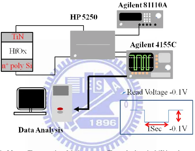
81110A, and the sweep and read measurement are accomplished by the Agilent 4155C. The pristine RRAM device exhibits a resistance > 108 Ω,namely, the read current of the pristine RRAM is beyond the limitation of the instrument. The pristine devices are subjected to a forming operation and then to the set/reset cycle. A positive voltage is applied to the top electrode of the device for forming/set operation and a negative voltage is applied to the top electrode during the reset operation. The bottom electrode is always grounded in each operation. The read voltage is -0.1V and the read time is 1sec in order to avoid the read disturbance [2.2]. The read operation will be applied to the top electrode of the device after the operation of forming/set/reset to confirm the resistance state of the RRAM device.
2.3 Current Compliance for Sweep Forming and Current
Overshoot
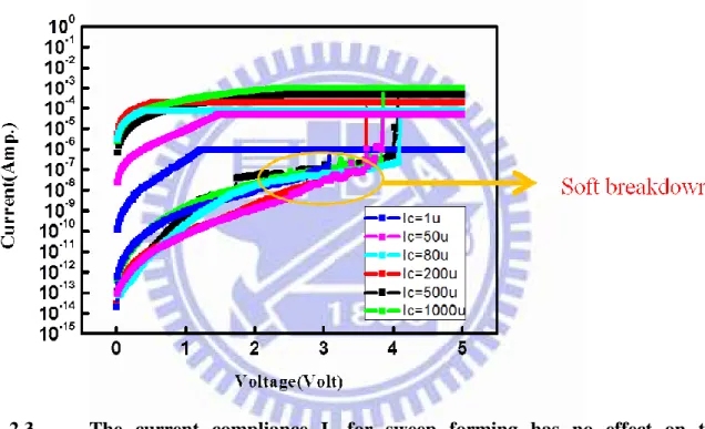
The result of the influence of current compliance on sweep forming is shown in Fig. 2.3. As shown in Fig. 2.3, the influence of the compliance current Ic on sweep forming is not
obvious when the Ic is larger than 80uA, that is, the current compliance Ic has no effect on the
resistance state after the forming process if the Ic is larger than 80uA. The forming would not
success if the compliance current is smaller than 80uA, the resistance state would be high because of the incomplete conducting filament. The resistance states are close after a successful forming, about 10kΩ according to the ohmic conduction behavior (I∝V) in a
low-voltage regime [2.2].
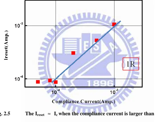
The current overshoot refers to the origin of the result that reset current is larger than the forming/set compliance current; the Ireset ≈ Ic when the current overshoot is negligible
8
shown in Fig. 2.5, the Ireset ≈ Ic when the compliance current is larger than 80uA. The soft
breakdown during the forming/set operation with leaky current may reduce the effect of current overshoot [2.4], and the law of Ireset ≈ Ic can extend down as shown in Fig. 2.4(b).
2.4 Sweep and Pulse Operation for Forming/Set/Reset
2.4.1
Sweep Forming & Sweep Set/Reset
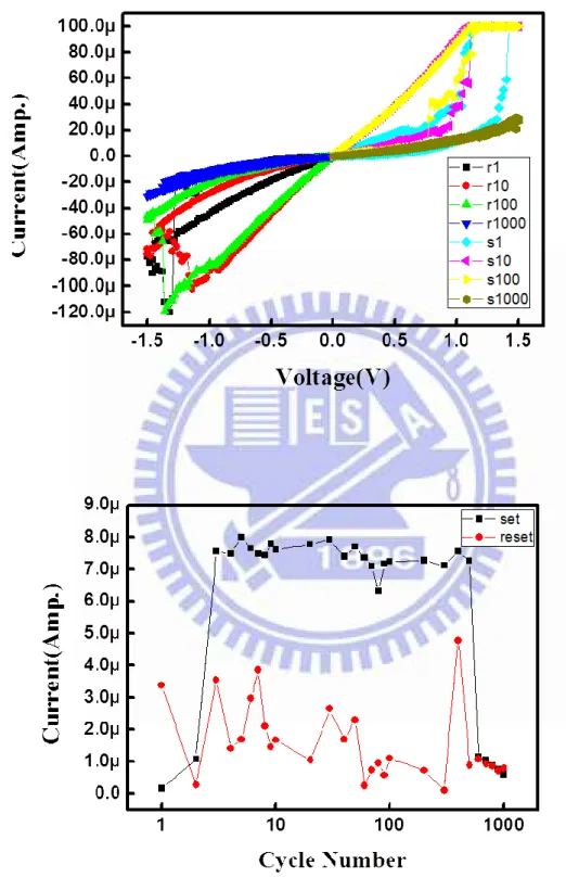
The result of sweep forming & sweep set/reset is shown in Fig. 2.6. The hysteresis phenomenon is obvious but the memory window is narrow. For forming process, the voltage is swept from 0V → 5V → 0V; for set process the voltage is swept from 0V → 1.5V → 0V; for reset process the voltage is swept from 0V → -1.5V → 0V. The sweep operation is a slow process, the time of process is much longer than that in pulse operation, but the applied voltage is much smaller than that in pulse operation, this is the voltage-time dilemma of RRAM [2.5].
2.4.2
Pulse Forming & Pulse Set/Reset
The pulse forming and pulse set/reset operation may cause several complex results, as shown in Fig. 2.7. The complex results of operation may come from the pulse forming operation. The locations of oxygen vacancies of the conducting filaments are mostly generated at the weak points along the grain boundary [2.6]. For the sweep forming, the long process time and the moderate increase of voltage make the oxygen vacancies Vo be generated step by step along the grain boundary and form a complete conducting filament finally; For the pulse forming, a sharp pulse wave is applied to the pristine device with high energy, this may cause the result of widespread Vo in the HfOx layer. The incomplete conducting filaments may cause a complex result of set/reset operation.
9
2.4.3
Sweep Forming & Pulse Set/Reset
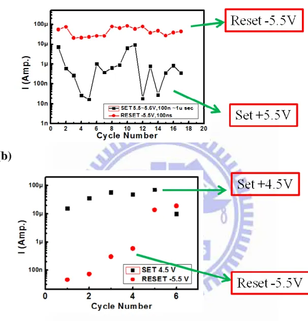
The combination of sweep forming and pulse set/reset has excellent performance as shown in Fig. 2.8. Under this method of operation, the memory window can extend from one order to four orders. The LRS for pulse are close since the LRS current is decided by the size of conducting filament; The HRS are scattered since each reset operation would recombine the oxygen vacancies Vo randomly.
For sweep forming and pulse set/reset operation, the sweep forming process provide a complete conducting filament and let the pulse set/reset operation drive the oxygen ions through the CF properly. Finally, the sweep forming and pulse set/reset operation is chosen to measured the RTN amplitude in chapter 3.
10
Fig. 2.1 Illustration of the device in this chapter. The top electrode is TiN, bottom electrode is n+ poly Si, and the HfOx is sandwiched between the electrodes with Height: 60Å Width: 0.6um Length: 0.6um.
11
Fig. 2.2 The connection of the instruments. The read voltage is -0.1V in order
12
Fig. 2.3 The current compliance Ic for sweep forming has no effect on the
resistance after the forming process if the Ic is larger than a threshold
13
(a)
(b)
Fig. 2.4 (a) Current overshoot induces the result that the reset current is larger than compliance current [2.3].
14
15
(a)
(b)
Fig. 2.6 (a) Sweep set/reset cycles, the hysteresis phenomenon is obvious.
(b) The memory window is small and it becomes closed when cycle times go over 600.
16
(a)
(b)
Fig. 2.7 (a) A reverse operation result due to pulse forming. (b) A normal operation result for pulse forming.
17
Fig. 2.8 The memory window and endurance of sweep forming& pulse
18
Chapter 3
RTN Main Distribution in HfOx-based RRAM
3.1 Introduction
The oxygen vacancies Vo may occupy the entire dielectric layer, most of the vacancies stay closed along the grain boundary to form the conducting filaments [3.1], some of the vacancies may appear near the conducting filaments as the random telegraph noise traps as shown in Fig. 3.1. The fluctuation of the read current due to the random telegraph noise may
induce the read failure in the memory applications. The amplitude of RTN is defined as I I
∆
where the ∆I is the difference between the Ihigh and Ilow, and the I at the denominator is the
Ihigh. As shown in Fig. 3.2, multi-level RTN phenomenon is easy to observe in the RRAM
devices, the amplitude of the RTN is related to the resistance states of the RRAM devices. The distributions of RTN amplitude have been analyzed in different resistance states with Weibull plot in 30Å and 60Å HfOx RRAM devices.
3.2 RTN Distributions in RRAM
The RTN distributions in each current level are shown in Fig. 3.3, the distributions split at the region of small amplitude. For the distributions in HRS, the distribution follows a straight line as exponential when the amplitude is smaller than a specific value and remains a tail in high amplitude region. To eliminate the effects of the tails on the main distributions, the tails are removed. There is no effect on the slope of the main distributions when the tails are removed in different amplitude as shown in Fig. 3.4.
19
The RTN distributions in different current levels in 60Å RRAM devices with tail removed are shown in Fig. 3.5(a), we remove the samples of RTN amplitude which are larger than 40% in current order E-8 and 20% in current order E-7 and 10% in current order E-6. The distributions split and follow straight lines in each current order and the average of the RTN amplitude increase with the resistance states as shown in Fig. 3.5(b). For 30Å RRAM devices, the RTN main distributions with tail removed are shown in Fig. 3.6(a), we remove the samples of RTN amplitude which are larger than 10% in each current level. The increase of the average with the resistance states is much smaller than that in 60Å devices as shown in Fig. 3.6(b).
3.3 RTN Main Distributions with Weibull Analysis in 60Å and
30Å RRAM
The RTN main distributions follow straight line and split in each current level, so we assume the function form of the cumulative density function as below
( / )
1
−
CDF x
( )
=
e
− x λ k E q . ( 3 . 1 ) And we transfer the eq.(3.1) asln(1
CDF x
( ))
( / )
x
λ
k−
−
=
E q . ( 3 . 2 )To identify the value of shape parameter k and scale parameter λ in the equation, we transfer the eq. (3.2) as
20
ln( ln(1
−
−
CDF x
( )))
=
k
ln
x
−
k
ln
λ
E q . ( 3 . 3 ) The Weibull plot of the 60Å HfOx RRAM device is shown in Fig. 3.7 and the Weibull plot of the 30Å HfOx RRAM device is shown in Fig. 3.8. The bending part of the Weibull plots in 60Å and 30Å RRAM come from the limitation of the resolution of instruments and the RTN amplitude that we can not recognize. The distributions for 60Å RRAM in Weibull plot seem to be parallel and equidistant between each current level, but the distributions for 30Å RRAM in Weibull plot seem to be less correlative between each current level. According to eq. (3.3), we can find out the shape parameter k and the scale parameter λ in each current level, and the result of 60Å RRAM is in Table I, the result of 30Å RRAM is in Table II. The rebuild distributions according to the parameters are shown in Fig. 3.9, the distributions are fitting well in both 60Å and 30Å RRAM.For 60Å RRAM, the shape parameter k equals to 1 in each current level as shown in Table I, which means the main distributions follow a trend of exponent for every resistance states. Because the main distributions are exponential, the scale parameterλ is equals to the average of the distribution, and the average of the RTN amplitude increase about 2 times when the resistance state increase one order.
For 30Å RRAM, the shape parameter k is close to 1 in each current order but the value of scale parameterλ(average) are not similar to those in 60Å RRAM. The increase of the average with the resistance is much smaller than those in 60Å RRAM. To identify the difference, we compare the RTN amplitude I
I
21
60Å and 30Å RRAM devices are closed in each current level, but the increase of I
I
∆ with
resistance are much bigger in 60Å RRAM than that in 30Å as shown in Fig. 3.10. The component of current in 30Å RRAM may be different to the current in 60Å RRAM.
The comparisons between the 60Å RRAM and 30Å RRAM are shown in Fig.3.11 and Table III. The trend of the distributions is exponential in each resistance states in both 30Å and 60Å devices, but the distributions are more sensitive to the resistance of the RRAM in 60Å RRAM devices. The average of RTN amplitude increase rapidly with the resistance in a thick HfOx layer device, which means the RTN induced read failure is more serious in thick HfOx layer device as shown in Fig. 3.12.
22
Fig. 3.1 The oxygen vacancies may appear near the conducting filaments as
23
24
Fig. 3.3 The RTN distributions in different current levels. The distributions split at the region of small amplitude.
25
Fig. 3.4 There is no effect on the slope of the main distributions when the tails
26
(a)
(b)
Fig. 3.5 (a) The RTN main distributions split and follow a straight line in each current level.
27
(a)
(b)
Fig. 3.6 (a) The RTN main distributions in 30Å RRAM in each current order seem to be closed.
(b) The average of the RTN amplitude in 30Å RRAM increase lightly with the resistance states.
28
Fig. 3.7 The distributions of RTN amplitude in 60Å RRAM follow straight line
29
30
(a ) (b )
(c ) (d )
Fig. 3.9 (a) The distributions rebuild in 60Å RRAM.
(b) Distribution of Current order E-6 rebuild in 30Å RRAM. (c) Distribution of Current order E-7 rebuild in 30Å RRAM. (d) Distribution of Current order E-8 rebuild in 30Å RRAM.
31
(a )
(b )
Fig. 3.10 (a) The I
I
∆
increase lightly with resistance in 30Å RRAM in comparison with 60Å RRAM.
32
(a )
(b ) (c )
Fig. 3.11 (a) For current order E-6,,,,the RTN amplitude distribution with tail
removing seems to be very similar to each other for 30Å and 60Å devices.
(b)(c) The RTN amplitude distributions in 60Å devices are more larger than the RTN amplitude distributions in 30Å devices for the current order of E-7 and E-8.
33
34
Current Order
Shape parameter k
Scale parameter λ
E-5 1.02488 0.013803
E-6 1.02488 0.025665
E-7 1.02488 0.051569
E-8 1.02488 0.100974
35
Current Order
Shape parameter k
Scale parameter λ
E-6 1.077466 0.026156 E-7 1.148097 0.032455 E-8 1.193457 0.050712
36
Current
Order 60Å Average 30Å Average
E-6 0.025665 0.026156
E-7 0.051569 0.032455
E-8 0.100974 0.050712
37
Chapter 4
Conclusion
The current compliance has to be bigger than a threshold current for successful forming to ignore the issue of current overshoot. A comparison of operation method between 1) sweep forming and sweep set/reset and 2) pulse forming and pulse set/reset and 3) sweep forming and pulse set/reset is accomplished in chapter 1. The method of sweep forming and sweep set/reset induces a narrow memory window but good endurance; the method of pulse forming and pulse set/reset make a complex result of operations because of the unstable conducting filament which is constructed by pulse forming; the method of sweep forming and pulse set/reset can switch the resistance states in a large range and has good endurance. We choose the method of sweep forming and pulse set/reset to measure the RTN amplitude in different resistance states.
The RTN distributions have two distribution trends in high resistance state in both 30Å and 60Å HfOx-based RRAM devices. In 60Å HfOx-based RRAM, the RTN main distributions of each current order follow an exponential trend in plot of cumulative density function & amplitude. These distributions split apart between each current order, and the average of the RTN amplitude increase about 2 times when the resistance state increase one order. In 30Å HfOx-based RRAM, the distributions follow an exponential trend, but the average increase lightly with the increase of resistance. The RTN main distributions become less sensitive to the resistance state when the thickness of RRAM is scaling down. The memory state read failure can be avoid by scaling the thickness of the dielectric layer.
38
Reference
Chapter 1
[1.1] Lai, S., “Tunnel oxide and ETOXTM flash scaling limitation,” Nonvolatile Memory ‘Technology Conference, 1998. 1998 Proceedings. Seventh Biennial IEEE ,22-24 June 1998, Pages5 ~ 7
[1.2] Lai, S.K. "Floating gate memories: Moore's law continues", VLSI Technology, 2005. (VLSI-TSA-Tech). 2005 IEEE VLSI-TSA International Symposium on, On page(s): 74 – 77
[1.3] S. Mori et al., “Thickness Scaling Limitation Factors of ONO Interpoly Dielectric for Nonvolatile Memory Devices,” IEEE Trans. Electron Devices, vol. 43, pp. 47–53, 1996.
[1.4] I. Baek, et al., "Highly scalable nonvolatile resistive memory using simple binary oxide driven by asymmetric unipolar voltage pulses," in Electron Devices Meeting, 2004. IEDM Technical Digest. IEEE International, 2004, pp. 587-590.
[1.5] R. Waser, et al., "Redox‐ Based Resistive Switching Memories–Nanoionic Mechanisms, Prospects, and Challenges," Advanced Materials, vol. 21, pp. 2632-2663, 2009.
[1.6] G. Bersuker, et al., "Metal oxide RRAM switching mechanism based on conductive filament microscopic properties," in Electron Devices Meeting (IEDM), 2010 IEEE International, 2010, pp. 19.6. 1-19.6. 4.
[1.7] D. Ielmini, "Filamentary-switching model in RRAM for time, energy and scaling projections," in Electron Devices Meeting (IEDM), 2011 IEEE International, 2011, pp. 17.2.1-17.2.4.
[1.8] X. A. Tran, et al., "A High-Yield HfOx-Based Unipolar Resistive RAM Employing Ni Electrode Compatible With Si-Diode Selector for Crossbar Integration," Electron Device Letters, IEEE, vol. 32, pp. 396-398, 2011.
[1.9] S. Yu, et al., "Understanding metal oxide RRAM current overshoot and reliability using Kinetic Monte Carlo simulation," in Electron Devices Meeting (IEDM), 2012 IEEE International, 2012, pp. 26.1. 1-26.1. 4.
[1.10] K. Kinoshita, et al., "Reduction in the reset current in a resistive random access memory consisting of NiOx brought about by reducing a parasitic capacitance,"
39
Applied Physics Letters, vol. 93, pp. 033506-033506-3, 2008.
[1.11] S. Yu, et al., "Conduction mechanism of TiN/HfOx/Pt resistive switching memory: A trap-assisted-tunneling model," Applied Physics Letters, vol. 99, p. 063507, 2011. [1.12] D. Veksler, et al., "Methodology for the statistical evaluation of the effect of random
telegraph noise (RTN) on RRAM characteristics," in Electron Devices Meeting (IEDM), 2012 IEEE International, 2012, pp. 9.6. 1-9.6. 4.
Chapter 2
[2.1] B. Briggs, et al., "Influence of Copper on the Switching Properties of Hafnium Oxide-Based Resistive Memory," in MRS Proceedings, 2011.
[2.2] H. Lee, et al., "Low power and high speed bipolar switching with a thin reactive Ti buffer layer in robust HfO2 based RRAM," in Electron Devices Meeting, 2008. IEDM 2008. IEEE International, 2008, pp. 1-4.
[2.3] K. Kinoshita, et al., "Reduction in the reset current in a resistive random access memory consisting of NiOx brought about by reducing a parasitic capacitance," Applied Physics Letters, vol. 93, pp. 033506-033506-3, 2008.
[2.4] D. Gilmer, et al., "Effects of RRAM stack configuration on forming voltage and current overshoot," in Memory Workshop (IMW), 2011 3rd IEEE International, 2011, pp. 1-4.
[2.5] R. Waser, et al., "Redox‐ Based Resistive Switching Memories–Nanoionic Mechanisms, Prospects, and Challenges," Advanced Materials, vol. 21, pp. 2632-2663, 2009.
[2.6] G. Bersuker, et al., "Metal oxide RRAM switching mechanism based on conductive filament microscopic properties," in Electron Devices Meeting (IEDM), 2010 IEEE International, 2010, pp. 19.6. 1-19.6. 4.
Chapter 3
[3.1] G. Bersuker, et al., "Metal oxide RRAM switching mechanism based on conductive filament microscopic properties," in Electron Devices Meeting (IEDM), 2010 IEEE International, 2010, pp. 19.6. 1-19.6. 4.
40
![Fig. 1.1 Classification of the resistive switching effects which are considered for non-volatile memory applications [1.5]](https://thumb-ap.123doks.com/thumbv2/9libinfo/8556796.188363/13.892.175.691.313.807/classification-resistive-switching-effects-considered-volatile-memory-applications.webp)
![Fig. 1.2 Valence Change Systems [1.5].](https://thumb-ap.123doks.com/thumbv2/9libinfo/8556796.188363/14.892.169.708.219.878/fig-valence-change-systems.webp)
![Fig. 1.3 Illustration of the behavior of O 2- and Vo during set/reset process [1.9]](https://thumb-ap.123doks.com/thumbv2/9libinfo/8556796.188363/15.892.195.668.423.792/fig-illustration-behavior-o-vo-set-reset-process.webp)