Investigation of the Space Charge Effect in the Quantum Well Infrared
Photodetector
C.
H. Kuan, Y. F. Hsu, andM.
C .
Hsu
Department of Electrical EngineeringNational Taiwan University Taipei, Taiwan, R. 0. C. Abstract
The I-V and noise in quantum well infrared photodetectors are investigated. It's found two regimes are in sequence with
V and V2 dependence of the current. The noise power for the
second regime shows 13" dependence. Based on barrier space charge, the first regime is attributed to the transport of residual electrons in equilibrium. The second regime indicates that electron drift velocity and Concentration are both proportional to applied biases. All the results is explained with partial potential drop on wells to increase the Fermi level.
Introduction
Recently, there has been much interest in GaAsJAlGaAs quantum well infrared photodetectors (QWIP) in the 10-pm range [l-41. The transport mechanisms in the dark current have been investigated extensively. For the QWIP with thin barriers (- 20 nm), the sequential resonant tunneling dominates through the low and high field domains [ 5 ] . For wide barrier (- 30 nm) cases, thermionic emission dominates at low biases while the thermally assisted tunneling plays a major role at high biases [6, 71.
In order to cut down the dark current of the QWIP, one of the interesting subjects is to understand the detailed mechanics of the thermionic emission current. In this paper, we report that for the QWIP with 50-nm barriers, the thermionic emission current can be divided into two different regimes in sequence with V and V2 dependence of the current. It indicates that the electron emission rate of the thermionic emission current increases with temperatures and biases. A theoretical model based on the electric field produced by the space charge in the wells and barriers is given to explain the results. The voltage dependence of the current is due to the increment of both of the Fermi level relative to the well edge and the electron concentration in the barrier with the applied bias.
Experiments
A. Sample Structure
The investigated QWIP is composed of 31 periods of 5-nm
GaAs wells and 50-nm Alo.25Gao.75As barriers, and GaAs contact layers at both ends. The n-type doping density in the wells and contacts is 1.2 x lo'* ~ m - ~ . It is noted that the barrier width is thicker than the conventional one of 30 nm. The idea is that the thermally assisted tunneling current is primarily determined by the applied electric field and hence a thicker barrier width may enlarge the initiation bias voltage of the tunneling current. It is then easy to observe the other current components at lower biases.
B. I- V Chartacteristics
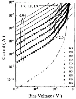
Fig. 1 shows the full-log I-V curves of the QWIP at different temperatures. It is apparent that there are three different regimes at temperatures between 61K and
81K.
The numbers in the figure represent the corresponding slope values. The first regime indicates I is approximately proportional to V. For the second regime, the slopes are 2.0 at lower temperatures and 1.7 at 81K. It implies that I is approximately proportional tov*.
1
,,
, , ; , l , : : l l ' l ; l ; , , , , , , I ,I l l 50K
10-10
Bias Voltage
(V
)Fig. 1 I-V curves of the QWIP at different temperatures. It is noted that the
current is divided into three different regimes between 61K and 81K.
25.6.1
The transition biases between the two regimes are found from the intersections of the two relationships. They are shown as the solid circles in the Fig. 5 and will be discussed later. At 50K, the seperation between the two regimes disappear. In the third regime, the exponential increment of the current is initiated at a fixed bias 3.5V. It is attributed to the thermally assisted tunneling and indicates the bias profile is independent of temperatures. We are interested to further investigate the first two regimes.
C. Noise Performance
Current ( A )
Figure 2 Noise PSD versus current at 69K. The dashed line represents the
associated noise PSD of the photoconductor. The solid squares are the data and the associated slope is 3/2.
Because the barrier may be considered as a resistor, the current through it is proportional to the product of the carrier concentration and drift velocity. To identify their bias dependence, we measure the noise characteristics of the current in the second regime at 69K. The results are shown as the solid squares in Fig. 2. The noise power spectral density (PSD) follows the 13” relationship as indicated by the solid line. The dashed line represents the general noise relationship of the photoconductor. The deviation indicates the different characteristics of the QWIP and the general photoconductor. The noise performance of the QWIP can also be described by the generation and recombination noise and the associated PSD is written as
Ai2 = 4egI = 4e(-pB&zf / L)Z (1)
where p~ is the electron mobility in the barrier, L the total
length of the QWIP, & the electrical field in the barrier, and zf
the electron lifetime [SI. The noise current gain is denoted by g and equal to the term in the parentheses. Here we have supposed the electron drift velocity is proportional to the electrical field. Since
Z
is proportional to Vz and & is approximately equal to-
V/(Nd) where N is the period number,and d the barrier width, g is hence proportional to 1’” in this regime and the PSD follows 13” relationship. Therefore the noise characteristics agree with the ZKV’ relationship and V dependence of the drift velocity. It can also be concluded here that the carrier concentration is proportional to V in the second regime of Fig. 1.
Analysis and Discussion A . Theoretical Model
In order to explain the results, we have derived a theoretical model based on the quasi-Fermi level in the barrier. The detailed derivation will be published in another paper, and here the important physical concepts and formulas are given ~91.
Scattering
Fig. 3 Band diagrams of the QWIP under (a) thermal equilibrium, and (b)
applied biases. In (b), the Fermi level in the barrier as indicated by the dashed line is higher than that in the well because of the scattered electrons
coming from the preceding wells.
As shown in Fig. 3, the Fermi level EF is flat at zero bias. The barrier electron concentration nB is given by nth = NC exp[(EB- E F ) / ~ T ] where Nc is the effective density of states in the barriers, and EB the barrier height. Under the external bias, the EF relative to the well edge is increased with edV and the
n B is increased with An = nth [exp(eAV/kT)
-
11. However,because of no doping in the barrier, the mean free path of the electrons is expected to be larger than the d. The increment of
nB may also result from the electrons generated by the neighboring wells with higher potential energies as shown in Fig. 3. Suppose the total increment is yAn (i.e., nB = nth + yAn)
where y is a fitting parameter to be extracted from the experimental data. If VB is the potential drop on a single barrier, then the total current is Z = nBepB(V$d)A where A is the cross sectional area of the QWIP.
To find out eAV, the electric field distributions have to be solved in advance. If the nB is small enough, the distribution is uniform and the quasi-Fermi level is a constant relative to the
25.6.2
conduction band edge even under biases. The electric field produced by the electron charge is hence derived. On the other hand, the wells are heavily doped and degenerate. The electrons can be regarded as three-dimensionally free carriers, or unmovable ones along the growth direction. The former well looks like a conductor while the latter does like an insulator. For these two cases, it is possible to find analytic solutions of the electric field in the well. Besides, by calculating the wave function of the self-consistent ground state of the well under external biases, the numerical result of the electric field can also be found. We will compare the results of these three cases.
For the three-dimensional free carriers and with the center of the well as the origin, the above mensioned procedure gives the potential energy U(x) in the well
u ( x ) = --evB -sinh
-
/ c o s h-
EW E B L D d (:D) ( 2 % ) ( 2 )
where and E W are the dielectric constants of the barrier and well respectively, and W the well width. The Debye length is Lo = ,/CykT E~ / ( e 2 N D ) where Cy is equal to 2F112(Y I F-,12(0,
6
= (EF-
EdlkT, and Ec the conductionband edge. The function F,,(x) is the Fermi-Dirac integral with the subscript n, i.e., F,(x) = ~ w y ” d y / ( l + e x p ( y - x ) ) . The calculated Debye length changes from 4.99 nm at 50K to 5.07 nm at 110K and is almost temperature independent. It is noted that because LD and W are compatible, the screening effect is
not strong and the potential energy profile in the well is similar to a triangle as that shown in Fig. 3.
0
results of the Fermi energy increment eAV by using the formulas for the insulator and free electrons for VB = 0 to 3V.
We also utilize the transfer matrix technique and the Poisson equation to calculate the self-consistent solution of the ground state in the well under the external applied bias. The positive ions for the donors in the well are assumed uniformly distributed. The eAV is extracted from the electric field produced b,y the ions and electrons. The differences among them are less than 8% at VB = 2.75V. Therefore, for the
electrons in the well, eAV can be estimated by (2) and is equal to -U( W 2 ) . From the same equation, the relationship between
V, and total applied bias V can also be found,
where CT is; a transform constant and equal to the term in the bracket.
Due to the increment of EF, and the assumption eAV <<
kT,
the current I may be written as
where Vtr is, the transition bias
+2?) ( 5 )
It is apparent that (4) can explain the two regimes found in Fig. 1. Besides, (3) and the almost independence of the Debye length on the temperature give a good reason why the thermally assisted tunneling current is initiated at a fixed bias at different temperatures.
B. Comparison with Experiments
4- insulator 4- 2D electron
-A- free electron
0.0 0.5 1.0 1.5 2.0 2.5 3.0
Extemal Bias(V)
Fig. 4 Fermi energy increment versus the external bias. There are three different cases. The case for the 2D electrons belong to the self-consistent
numerical calculation result. The other two are analytic solutions.
If we regard the well as an insulator, the potential energy profile is -(eVBEs)/(E&). Fig. 4 shows the calculation
Utilizing y in (5) as a parameter to fit the solid circles in Fig. 5 , we find that y is equal to 6.1 and the result is shown as the solid line. The y value indicates that the injected electrons from the preceding sixth well can contribute to the carrier concentration in the barrier. With (4) and I-V curves, the pB at different temperatures can be estimated and the results are shown as the solid triangles in Fig. 5. The dashed curve represents the mobility to follow the T3” dependence due to the scattering of the phonons. The measured electron Hall mobility at 77K for pure n-type GaAs sample is about 2 x lo5
cm2 / V-s [IO]. Our data show that the electron mobility in A10.25Ga071iAs barriers is about lo4 cm2 / V-s at the same temperature, which is a reasonable value [ 1 11.
IEDM 98-675
At 50K, the I-V curve does not have an apparent V2 dependent regime. It may be explained with (2). Taking V,
=
1.0/31 V_, T = 50K and E ~ / E ~ = 12.4/13.18, (2) gives eAV= 1.4 meV, which is equal to 0.33kT. The approximation of exp(eAV/kT) with (1
+
eAV/kT) is not appropriate for higher biases. Therefore, the data show higher than V2 dependence under the biases around 1 to 3.5V. From Fig. 2, the ratio of the noise power spectral density over 13” can be found. Combining (1) and (4) with the ratio, we find that the electron lifetime is 0.56 ps for our QWIP, which is close to the result measured by subpicosecond luminescence at 69K [ 121.0.9 h .
3
0.8 3-$
0.73
0.6 0 .- .... i : . 1.0, , 18 - --
- 0.51
A 1 1 65
144
0, A 0.4‘i o
’ Bo ’i o
’so
‘ 40 ’ I b O ’ 6 Temperature ( K )Fig. 5 Transition bias and mobility versus temperature. The solid circles represent the experimental results of transition biases while the solid line is
the theoretical values. The mobility as represented by solid triangles is derived from the conductance of the sample at low biases. The dashed curve shows temperature dependence of the mobility due to scattering of phonons.
The similar I-V characteristics also appear in the measurement of the resistivity of semi-insulating epitaxial layer [13]. The V dependent regime is explained with the thermal equilibrium electron concentration while V2 dependent one is with the high injection of carriers from the contact. In our QWIP case, the high injection is due to the increment of the Fermi level relative to the well edge by the applied bias.
Summary
concentration in the barrier increases with bias and temperature. It can be explained with our theoretical model in which the increment of the Fermi level with the applied bias renders the increment of the concentration.
This work was supported by the National Science Council of the Republic of China under contract number NSC 87- 22 15-E-002-005.
Reference
[I] L. C. West and S. J. Eglash, “First observation of an extremely large-
dipole infrared transition within the conduction band of a GaAs
quantum well,” Appl. Phys. Lett. Vol. 46, pp. 1156-1 158, June 1985.
[2] B. F. Levine, C. G. Bethea, G. Hasnain, V. 0. Shen, E. Pelve, R. R.
Abbott, and S. J. Hsieh, “High sensitivity low dark current 10 pm GaAs
quantum well infrared photodetectors,” Appl. Phys. Lett. Vol. 56, pp. 851-853, Febrary 1990.
[3] J. Y. Anderson and L. Lundquivst, “Near-unity quantum efficiency of
AIGaAs/GaAs quantum well infrared detectors using a waceguide with a doubly periodic granting coupler,” Appl. Phys. Lett. Vol. 59, pp. 857- 859, June 1991.
[4] L. S. Yu and S. S. Li, “A metal grating coupled bound-to-miniband transition GaAs multiquantum well/superlattice infrared detector,” Appl. Phys. Lett. Vol. 59, pp. 1332-1334 September 1991.
[5] K. K. Choi, B. F. Levine, R. J. Malik, J. Walker, and C. G. Bethea,
“ Periodic negative conductance by sequential resonant tunneling
through an expanding high-field superlattice domain,” Phys. Rev. B
[6] E. Pelve, F. Beltram, C. G. Bethea, B. F. Levine, V. 0. Shen, S. J. Hsieh, and R. R. Abbott, “Analysis of the dark current in doped-well
multiple quantum well AlGaAs infrared photodetectors,” J. Appl.
Phys. Vol. 66, pp. 5656-5658, December 1989.
[7] C. H. Kuan, D. C. Tsui, K. K. Choi, P. G. Newman, and W. H. Chang, “Hot-electron distribution in multiple quantum well infrared
photodetectors,” Appl. Phys. Lett. Vol. 63, pp. 2091-2093, October
1993.
[8] A. Rose, Concepts in Photoconductivity and Applied Problems
(Interscience, New York, 1963).
191 C. H. Kuan and C. C. Chen. “Electron Transport Mechanism Before
Tunneling in the Quantum Well Infrared Photodetector” (unpublished).
[lo] J. S. Blakemore, “Semiconducting and other major properties of
gallium arsenide,” J. Appl. Phys., Vol. 53, pp. 123-181, 1982. [l 11 W. C. Liu, “Investigation of electrical and photoluminescent properties
of MBE grown AI,Gal.,As layers,” J. Materials Science, Vol. 25, pp,
[I21 B. Deveaud, A. Chomette, F. Clerot, and Regreny, Intersubband
Transitions in Quantum Well, edited by Emmanuel Rosencher etc., Plenum Press, New York, 1992.
[13] V. Swaminathan and A. T. Macrander, Materials Aspects ofGaAs and
InP BasedStructure, pp. 255-261 (Prentica Hall, New Jersey, 1991).
Vol. 35, pp. 4172-4175, March 1987.
1765-1772, March 1990.
In summary, the I-V characteristics and noise performance before electron tunneling in our QWIP show the electron