and Department of Electrical Engineering, National Taiwan University, Taipei, Taiwan 10617, Republic of China
共Received 24 February 2007; accepted 6 August 2007; published online 3 October 2007兲
Formation of Pt nanoparticles or nanoisland films as a function of annealing temperature, initial thickness, underlying substrates, and annealing process is investigated. Using microphoto-luminescence 共PL兲 measurement, we find great enhancement of self-emission in visible spectrum from Pt nanoparticles. The integral intensity of the micro-PL of the 49.38 nm Pt nanoparticles is 38 times of that of the Pt thin film. In addition, the peak wavelength varies from 554 to 615 nm as the surface morphology of Pt changes due to different annealing parameters. Spectral analyses suggest that this enhancement of micro-PL from Pt is due to the local field enhancement mechanism analogous to that of PL from noble metals. © 2007 American Institute of Physics.
关DOI:10.1063/1.2785942兴
I. INTRODUCTION
The unique optical properties of roughened metal sur-faces or metal nanoparticles, especially of noble metals such as gold, silver, and copper, have been intensively studied over the past few decades. For instance, gold exhibits par-ticular absorption peaks at visible wavelengths due to surface plasmon resonance共SPR兲 as its size is reduced to nanometer dimensions.1 The Raman scattering of rhodamine 6G or other organic molecules adsorbed on aggregated Ag colloids can also be greatly enhanced.2This is the well-known phe-nomenon called surface enhanced Raman scattering共SERS兲. Enhanced photoluminescence from noble metal nanopar-ticles has also been observed and has attracted much attention.3 Theoretical work has previously demonstrated that the photoluminescence共PL兲 of noble metals is the direct recombination of the conduction-band electrons near the Fermi level with the holes in the d band.4However, the PL intensity of noble metals is very weak. The PL efficiency of smooth gold explored by Mooradian’s original experiment was on the order of 10−10. One possible reason for this low
PL efficiency is that the nonradiative energy relaxation pro-cesses of photoexcited carriers in metals, such as Coulomb carrier-carrier scattering, are much faster than radiative electron-hole recombination, thus quenching the PL.5 How-ever, when noble metals are reduced to sizes in the range of nanometers, PL efficiency can be enhanced by about
104– 106 times.6 PL enhancement based on the phenomeno-logical model by Boyd et al.7 has been considered due to local field enhancement. Nonetheless, some scientists have developed different ideas in recent years. Dulkeith et al. ex-plained a process in which the excited d-band holes recom-bined with the sp electrons emitting plasmons. These plas-mons subsequently radiated, giving rise to PL.8
For transition metals, previous investigation has shown that their optical properties when they are several nanometers in size cannot be enhanced as significantly as those observed in Au, Ag, and Cu.9However, many applications and studies have been focused on them, particularly on Pt, which has been often used as electrode material. For example, rough-ened platinum electrodes can enhance the Raman scattering of pyridine10 or other organic molecules; platinum island films can also enhance light absorption of some materials, such as infrared absorption of p-NTP.11A recent report dem-onstrated that Pt nanoparticles sputtered on ZnO can greatly enhance the bandgap emission of ZnO nanorods.12 In this paper, we present an annealing method for fabricating Pt nanoisland films and nanoparticles of different sizes. The for-mation of nanoscale Pt particles as a function of temperature, film thickness, underlying substrates, and annealing process is reported. We have observed that the peak wavelength of surface enhanced micro-PL of Pt was shifted by the changes in the particles’ shapes. X-ray photoelectron spectroscopy 共XPS兲 and X-ray diffraction 共XRD兲 were utilized to examine the composition of our samples. In order to observe the sur-face plasmon effect on our samples, the extinction spectra of Pt nanoisland films were measured.
a兲Author to whom correspondence should be addressed. Telephone:
886-2-3366 3540. FAX: 886-2-2364 2603. Electronic mail: [email protected]
II. EXPERIMENT
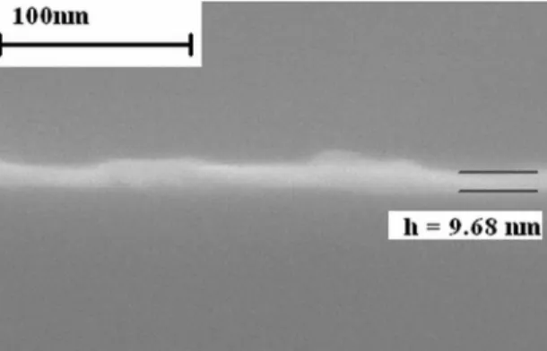
We produced our samples using platinum nanoparticles or nanoisland films on Si or quartz substrates. Si substrates were initially cleaned by acetone, methanol, and de-ionized water sequentially. Then, spin-on glass共SOG兲 31F was spun on silicon substrates. The platinum film was deposited on SOG film by electron-gun evaporation at 1.8⫻10−6torr. The deposition rate was estimated to be 0.01 nm/ s. The scanning electron microscopy共SEM兲 photo of the unannealed Pt film is shown in Fig.1. Its thickness is about 10 nm. The samples with the Pt thin film were then annealed at different tempera-tures. Different annealing apparatuses had also been tested. One used the rapid thermal annealing共RTA兲 with N2purging 共RTA process兲 and the other used a heating stage in a cham-ber under a pressure of 10−3torr共vacuum process兲. The
pur-pose of the SOG film spun on the silicon substrates was to prevent the formation of PtSi alloy or other platinum sili-cides when the Pt thin film was annealed.13The samples on the quartz substrates were prepared by the same procedure as those on the Si substrates. After annealing for 5 min, Pt is-lands in the nanometer range were formed. The morphology and size distribution of the Pt nanoisland films were investi-gated using SEM. Micro-PL spectra of Pt nanoisland films were measured using excitation from a 514.5 nm Ar+ laser focused through a microscope. The radiative emission was dispersed by a monochromator and detected by a cooled pho-tomultiplier tube 共PMT兲. The XRD studies were measured with a Cu K␣line and the XPS studies were carried out with an Mg K␣X-ray source共1253.6 eV兲. The extinction spectra of the platinum nanoisland films were also measured for the samples fabricated on the quartz substrates by a spectropho-tometer with a resolution of 0.5 nm.
III. RESULTS AND DISCUSSION
SiO2 has a thermal expansion coefficient of 0.5 ⫻10−6/ K, which is much smaller than the thermal expansion
coefficient of Pt films共8.8⫻10−6/ K兲. This would induce
sig-nificant compressive stress in Pt共Ref. 14兲 when the Pt thin
films were annealed. If the initial thickness of the metal is in the scale of nanometers, the compressive stress would cause the metal to form isolated islands.15In our works, the thick-ness of the Pt films and the annealing temperature have been varied to produce Pt nanoparticles and Pt nanoisland films with different sized particle. Figure2shows the SEM photos
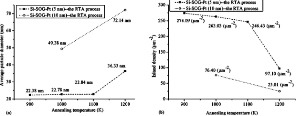
of Pt nanoparticles and Pt nanoisland films with different sized particle. Figures2共a兲–2共c兲are the SEM pictures of the 5 nm Pt thin film on the Si substrate annealed by the RTA process at 1000, 1100, and 1200 K, respectively. We found that the particle sizes increase with the annealing tempera-ture. Figures2共d兲and2共e兲are the SEM pictures of the 10 nm Pt thin film on the Si substrate annealed by the RTA process at 1000 and 1200 K, respectively. They also reveal that the particle sizes formed at the higher temperature are larger than those formed at the lower temperature. Annealing at the high temperature allows mass transport of small clusters across the surface to form larger clusters in a process analo-gous to the Ostwald ripening mechanism.16,17 Island forma-tion mechanism analogous to Ostwald ripening could also be observed in our experiments. Figures 3共a兲 and 3共b兲 show feature variation in the surface morphology with the anneal-ing temperature for those samples shown in Figs.2共a兲–2共e兲. Figure3共a兲demonstrates that average particle sizes increase with annealing temperature regardless whether the initial thickness of Pt is 5 or 10 nm. Figure3共b兲 shows that island
FIG. 1. SEM picture of unannealed Pt film.
FIG. 2. SEM pictures of Pt nanoparticles and nanoisland films by different annealing methods.关共a兲–共c兲兴 5 nm Pt thin film on the Si substrate annealed by the RTA process at 100, 1000, and 1200 K, respectively.关共d兲 and 共e兲兴 10 nm Pt thin film on Si substrate annealed by the RTA process at 1000 and 1200 K, respectively.共f兲 10 nm Pt thin film on Si substrate annealed by the vacuum process at 1000 K.共g兲 10 nm Pt thin film on quartz substrate an-nealed by the vacuum process at 1000 K.共h兲 10 nm Pt thin film on quartz substrate annealed by the RTA process at 1000 K.
density decreases with annealing temperature as well. It is clear that high annealing temperatures increase average par-ticle size and reduce island density. Furthermore, Figs.3共a兲 and 3共b兲 show that particle size suddenly increases and is-land density suddenly decreases at annealing temperatures above 1100 K for the Pt nanoparticles prepared with the 5 nm initial thickness. This may be attributed to surface melting of nanoparticles.18 The fact that nanoparticle size remains at around 23 nm and then abruptly increases to 36 nm after 1100 K indicates that the melting point of the Pt nanoparticles with average diameter of 23 nm might be around 1100 K.
It is known that the initial thickness of the metal films can play an important role in determining their surface mor-phology at a given temperature.19From Fig.3共a兲, the average diameter of the 5 nm initial thickness of Pt annealed at 1000 K is 22.78 nm. This is smaller than the 49.38 nm Pt nanoparticles prepared with 10 nm initial thickness. Figure
3共b兲shows that when Pt thin film is annealed at 1000 K, the island densities are 263.03m−2 for the sample with 5 nm
initial thickness and 76.40m−2 for the sample with 10 nm
initial thickness. Similar results are shown in the Figs.3共a兲 and3共b兲 in which the samples were annealed at 1200 K as well. The thinner the initial film is, the larger the particle sizes and the higher the island density that are formed.
Previous studies have shown that the sizes of the metal islands are affected by different types of substrates6,20 and different ambiences during the annealing process.21 We in-vestigated two processes, the vacuum process and the RTA process, and two different types of substrates, Si and quartz. Figures2共f兲and2共g兲, respectively, show the SEM photos of the 10 nm Pt thin film on the Si substrate and the quartz substrate annealed by the vacuum process at 1000 K. Figures
2共d兲 and 2共h兲, respectively, show the SEM photos of the 10 nm Pt thin film on the Si substrate and the quartz sub-strate annealed by the RTA process at 1000 K. Our
experi-ments show that the island density of the Pt nanoisland films on quartz substrates is smaller than that on Si substrates both using the RTA and the vacuum process. In addition, the vacuum process results in a smaller island density than the RTA process, as shown in TableI.
The micro-PL of the Pt nanoparticles and the Pt nanois-land films was measured under the excitation of a 514.5 nm Ar+ laser. Figure 4 shows the micro-PL spectra of several samples. Curves 共a兲–共c兲 are the micro-PL spectra of the Pt nanoparticles of different sizes prepared under different con-ditions. Curve共d兲 is the micro-PL of the sample of only SOG on Si without Pt. Curve共e兲 is the micro-PL spectrum of the 10 nm Pt thin film on Si substrate but without annealing. Curves 共d兲 and 共e兲 are shown together for comparison. The luminescence from the Pt nanoparticles is largely enhanced, when compared to the spectrum of the 10 nm Pt thin film without annealing. For instance, the integral intensity of the 49.38 nm Pt nanoparticles with the micro-PL spectrum shown by curve共a兲 in Fig.4 is about 38 times of that of the sample with the 10 nm Pt thin film but without annealing. We also found that the peak wavelength of the micro-PL spectra of the Pt nanoparticles varies with their surface mor-phology. Similar phenomena have also been observed from gold nanoparticles and nanorods in previous studies.22–24 It has been demonstrated that the PL enhancement of noble metal nanoparticles or rough surfaces is due to local field enhancement.7,22 Local field enhancement includes two parts: One is the collective oscillation of electrons in surface protrusions which can be induced by the optical field. This is referred to as the local plasmon effect. The other is that field tends to concentrate at the tips of surface protrusions. This is known as the lightning rod effect, which is the reason for the redshift of emission peaks with the increasing aspect ratio of nanorods.7,22,23From our results, as shown in Fig.4, we find that the peak wavelengths of curves共a兲 and 共b兲 are close to 554 nm, but the peak wavelength of curve共c兲 is significantly
TABLE I. Island formation conditions using the RTA and the vacuum processes.
Substrates Initial thickness 共nm兲 Annealing temperature 共K兲 Process Island density 共m−2兲 SEM image Si 10 1000 RTA 76.40 Fig.2共d兲 Si 10 1000 Vacuum 9.51 Fig.2共f兲
Quartz 10 1000 Vacuum 9.12 Fig.2共g兲
redshifted to 610 nm. The particles whose micro-PL spectra are shown in Figs.4共a兲and4共b兲are almost round in shape. The aspect ratio of the Pt nanoparticles is obviously smaller than that of the Pt nanoisland films. As a result, the redshift of the peak wavelength of the micro-PL from the Pt nanois-land films is to be expected. We suggest that the variation of the peak wavelength of the micro-PL from Pt is due to the lightning rod effect.
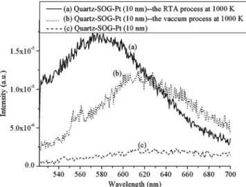
The enhanced micro-PL of Pt can be found in the Pt nanoisland films on the quartz substrates as well, as shown in Fig.5In Figs.5共a兲and5共b兲are shown the micro-PL spectra of the Pt nanoisland film formed by the RTA process and the vacuum process, respectively. Curve 共c兲 is the micro-PL spectra of the 10 nm Pt thin film on the quartz substrate without annealing. From Fig. 5, the integral intensity of the micro-PL spectrum shown by curve共a兲 for the Pt nanoisland film 共island density of 26.84m−2兲 is about eight times of
that of the sample with the 10 nm Pt thin film without an-nealing. In addition, the variation of the peak wavelength of the micro-PL due to different surface morphologies of Pt can be found. The peak wavelength of the micro-PL of the Pt nanoisland film annealed by the RTA process is about 576 nm, and for the sample annealed by the vacuum process, it is close to 615 nm. Figure6shows the micro-PL spectra of the samples with 5 nm initial thickness of Pt annealed at different temperatures. Curves 共a兲–共c兲 in Fig. 6 show the samples annealed by the RTA process at 1200, 1100, and 1000 K, respectively. The peak wavelengths of the micro-PL spectra are all close to 554 nm. This is due to the fact that the particles of the samples with the 5 nm initial thickness of Pt annealed at temperatures higher than 1000 K are almost round. This micro-PL is significantly enhanced by the Pt na-nomorphology.
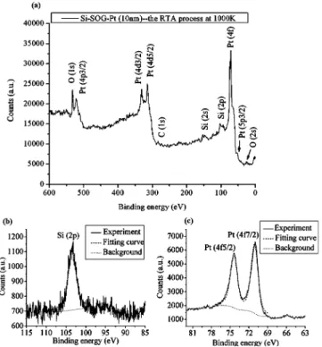
Similar results showing intense fluorescence from transition-metal nanoparticles such as Fe have been reported.25 The authors suggest that the partial oxidation of metal nanoparticles possibly occur on the metal’s surface. These metal oxide clusters are photoactivated and might give rise to the observed fluorescence. In order to confirm the composition of the Pt nanoparticles and the nanoisland films, the XPS and XRD measurements are utilized. The XPS stud-ies were carried out with a Mg K␣x-ray source共1253.6 eV兲. One of our samples’ XPS spectra is shown in Fig. 7. This illustrates the sample with 10 nm Pt thin film annealed by the RTA process at 1000 K. The XPS peaks in Fig.7 are refer-enced to the C 1s binding energy of the adventitious carbon at 284.5 eV. Figure 7共a兲 is the XPS spectrum in the range between 0 and 600 eV. All the peaks are labeled and reveal that three elements, Pt, Si, and O, exist at the surface of the samples. To get a clear view, the XPS spectrums of Si 2p and Pt 4f are plotted in Figs. 7共b兲 and7共c兲, respectively. From Fig.7共b兲, the peak of Si 2p is at 103.43 eV, which is origi-nated from the SOG film under the Pt nanoparticles. From Fig.7共c兲, the peak of Pt 4f7/2is at 71.11 eV. The fact that the
binding energy of the Pt 4f7/2peak for the bulk Pt measured FIG. 4. The micro-PL spectra of samples on Si substrates with共a兲 the 10 nm
Pt thin film annealed by the RTA process at 1000 K,共b兲 the 5 nm Pt thin film annealed by the RTA process at 1000 K, 共c兲 the 10 nm Pt thin film annealed by the vacuum process at 1000 K,共d兲 the SOG film, and 共e兲 the 10 nm Pt thin film without annealing.
FIG. 5. The micro-PL spectra of the samples on quartz substrates with共a兲 the 10 nm Pt thin film annealed by the RTA process at 1000 K,共b兲 the 10 nm Pt thin film annealed by the vacuum process at 1000 K, and共c兲 the 10 nm Pt thin film without annealing.
FIG. 6. The micro-PL spectra for the samples with 5 nm initial thickness annealed at different temperatures by the RTA process.共a兲 The annealing temperature is 1200 K.共b兲 The annealing temperature is 1100 K. 共c兲 The annealing temperature is 1000 K.
by the same instrument is 71.3 eV suggests that oxidation and silicide formation on Pt nanoparticles during annealing do not occur. Figure8shows the result of the XRD of the Pt nanoisland films on the quartz substrates annealed by differ-ent processes. Only the XRD signal corresponding to Pt 共111兲 is found. The broad XRD signal of a-PtOx共2= 32°兲 共Ref.26兲 and the XRD signals of PtSi or Pt2Si共Ref.27兲 are
not observed. The results show that the SOG films under the Pt thin film could prevent the formation of platinum silicide and platinum oxide during annealing. This result is in line with previous research.13 The investigation using the XPS and XRD measurements suggests that the composition of the
the Fermi level and over about 0.3 eV.28,29 Since the Cou-lomb carrier-carrier scattering time considerably depends on the density of states 共DOS兲 around the Fermi level, and the DOS around the Fermi level is enhanced by the d states in Pt, the lifetime of the photoexcited carriers is smaller in Pt than in noble metals.30 This significantly reduces the radiative electron-hole recombination in the smooth Pt film. For this reason, the signal of emission is very low and could not be easily detected from the Pt thin films in our experiment. However, as nanoparticles and the nanoisland films are formed after annealing, the efficiency of the light coming from Pt can be greatly improved because of the local field enhancement mechanism.
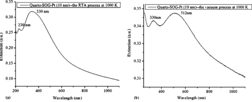
The extinction spectra of Pt nanoisland films on quartz substrates were measured to observe the localized surface plasmon effect in our samples with the quartz substrates. Localized surface plasmon resonance 共LSPR兲 is the excita-tion of collective resonance of conducexcita-tion electrons induced by electromagnetic radiation.31–33 The frequency of the LSPR can be tuned by changing the size, shape, and dielec-tric constant of the surrounding medium.31–33 For platinum, previous studies had shown that the frequency of the LSPR is located in the ultraviolet light region.13,22Nonetheless, re-cently, Langhammer et al.33reported that the extinction peak of a Pt nanodisk would shift from 200 to 1800 nm as the diameters varied from 38 to 530 nm. Figures 9共a兲 and9共b兲 are the extinction spectra of the samples with the 10 nm Pt thin film annealed by the RTA and the vacuum processes at 1000 K. The SOG film on the quartz substrate is used as a reference, indicating that the extinction features result from the platinum nanoisland films. Figure 9共a兲shows that there are extinction peaks at 230 and 330 nm for the sample an-nealed by the RTA process at 1000 K. Figure9共b兲shows that the extinction peaks are at 330 and 512 nm for the sample annealed by the vacuum process at 1000 K. These peaks are referred to as the frequency of the LSPR of the Pt nanoisland films. The characteristics of the two peaks in the extinction spectra might be attributed to the resonant frequency of the transverse and the longitudinal plasmon oscillation.22–24 Since the frequency of the LSPR of metal nanostructures is redshifted with increasing particle size and aspect ratio,22–24,33 the extinction spectra in Figs. 9共a兲and9共b兲 re-veal that the particle size and the aspect ratio of the Pt nanoisland films annealed by the vacuum process are larger than those of the Pt nanoisland films annealed by the RTA process. This result corresponds to their surface morphology, as shown in the SEM pictures关Figs.2共g兲and2共h兲兴 and their micro-PL behaviors 关curves 共a兲 and 共b兲 in Fig. 5兴. In
addi-FIG. 7. The XPS spectra for the sample with the 10 nm Pt thin film an-nealed by the RTA process at 1000 K.共a兲 The XPS spectrum in the range of 0 – 600 eV.共b兲 The XPS spectrum for Si 2p. 共c兲 The XPS spectrum for Pt 4f.
FIG. 8. The XRD spectra of the Pt nanoisland films annealed by different processes. Only the peak corresponding to Pt共111兲 is found.
tion, we could not find a peak near 1.2– 1.4 eV from the extinction spectra, which is assigned to the absorption peak of PtOx.34,35 We can confirm that the extinction features re-sult from the surface morphology of Pt.
Some research has suggested that the PL of noble metals might be related to the resonance of surface plasmon. Dulkeith et al.8 reported that the emission spectra of gold nanoparticles could coincide with their extinction spectra ac-cording to the Mie theory, so they stated that PL enhance-ment should be due to the emission of particle plasmons. Mohamed et al.23 suggested that the relaxation of surface plasmon coherent electronic motions followed by the recom-bination of the d-band holes and the sp-band electrons lead to the enhanced PL of gold since the wavelength of the LSPR was close to that of their excitation laser. However, Var-navski et al.24 found that the luminescence efficiency is the same for gold nanospheres 共with a surface plasmon reso-nance of 520 nm兲 when using an excitation laser at 4.65 and 3.02 eV. Their experimental results are inconsistent with the suggestion that the observed emission is due to surface plas-mon emission or surface plasplas-mon excitation by incoming light. They reported that the emission originated from the
sp-electron/d-hole recombination with the enhancement of
the incoming and outgoing fields via the local field enhance-ment mechanism. From our extinction spectra, as shown in Fig.9, one of the LSPR for the Pt nanoisland films annealed by the vacuum process is 512 nm. This is close to the wave-length of our excitation laser 共514.5 nm兲. This result shows the possibility that the micro-PL enhancement could be re-lated to the excitation of the LSPR. However, for the sample annealed by the RTA process, the LSPR differs greatly from the wavelength of our excitation laser and the peak position of the micro-PL. If the observed micro-PL comes from LSPR excitation, the signal of micro-PL from the sample annealed by the vacuum process should be larger than that from the sample annealed by the RTA process. Nevertheless, our ex-perimental results contradict this. The integral intensity of the micro-PL for the sample annealed by the vacuum process is lower than that of the sample annealed by the RTA pro-cess. These results reveal that the observed micro-PL of Pt would not be significantly influenced by the behaviors of the LSPR. The excitation of the LSPR might contribute to the enhancement of micro-PL for the sample annealed by the vacuum process, but whether the LSPR is crucial to the ob-served micro-PL could not be easily confirmed by our
inves-tigation. As a result, we suggest that the observed micro-PL of Pt is attributed to the local field enhancement of the in-coming and outgoing fields.
IV. CONCLUSIONS
In summary, we used the annealing process to produce Pt nanoparticles or Pt nanoisland films of different sizes as a function of temperature, film thickness, pressure, and under-lying substrates. The high annealing temperature caused par-ticle size to increase and island density to decrease. Increas-ing the initial thickness of Pt from 5 to 10 nm, we found that the particle sizes doubled and island density was reduced. The quartz substrates resulted in a smaller island density than the Si substrates and the vacuum process produced a smaller island density than the RTA process. Furthermore, our ex-periment suggests that the melting point of the 23 nm Pt nanoparticles is about 1100 K. In addition, we found that the surface enhanced micro-PL of Pt is analogous to the PL of noble metal nanoparticles. The integral intensity of the micro-PL of the 49.38 nm Pt nanoparticles is 38 times of that of the Pt thin film. The peak wavelength of the micro-PL of the Pt nanoparticles varied from 554 to 615 nm as a result of the change in the Pt surface morphology. Extinction spectra show that the frequency of the LSPR for the Pt nanoisland film annealed by the RTA process is at 230 and 330 nm. Those peaks redshift to 330 and 512 nm for the Pt nanois-land film annealed by the vacuum process. The redshift of the extinction peaks reveals that the particle size and the aspect ratio of the Pt nanoisland film annealed by the vacuum process are larger than those of the Pt nanoisalnd film annealed by the RTA process. This result corresponds to their surface morphology, as shown by the SEM pictures and their micro-PL behaviors. From our studies of the XPS and the XRD, we suggest that the observed optical properties of the Pt nanoparticles and the nanoisland films are related to their surface morphology. Our results for the optical proper-ties of Pt nanoparticles measured by micro-PL and extinction could lead to a wide range of potential applications, includ-ing solar cells and surface enhanced Raman scatterinclud-ing. ACKNOWLEDGMENT
This work is supported by the National Science Council, Taiwan, Republic of China, with Grant Nos. NSC95-2120-M-002-001 and NSC95-2112-M-002-004.
FIG. 9. The extinction spectra of the samples on quartz substrates with共a兲 the 10 nm Pt thin film annealed by the RTA process at 1000 K and 共b兲 the 10 nm Pt thin film annealed by the vacuum process at 1000 K.
Tian, Surf. Sci. 406, 9共1998兲.
11A. E. Bjerke and P. R. Griffiths, Appl. Spectrosc. 56, 1275共2002兲. 12J. M. Lin, H. Y. Lin, C. L. Cheng, and Y. F. Chen, Nanotechnology 17,
4391共2006兲.
13E. Anno and M. Tanimoto, J. Appl. Phys. 88, 3426共2000兲.
14C. Bower, O. Zhou, W. Zhu, D. J. Werder, and S. Jin, Appl. Phys. Lett. 77,
2767共2000兲.
15J. A. Floro, S. J. Hearne, J. A. Hunter, P. Kotula, E. Chason, S. C. Seel,
and C. V. Thompson, J. Appl. Phys. 89, 4886共2001兲.
16J. D. Carey, L. L. Ong, and S. R. P. Silva, Nanotechnology 14, 1223
共2003兲.
17S. Wei, B. Li, T. Fujimoto, and I. Kojima, Phys. Rev. B 58, 3605共1998兲. 18Z. L. Wang, J. M. Petroski, T. C. Green, and M. A. El-Sayed, J. Phys.
Chem. B 102, 6145共1998兲.
27A. A. Naem, J. Appl. Phys. 64, 4161共1988兲. 28N. V. Smith, Phys. Rev. B 9, 1365共1974兲.
29R. E. Dietz, E. G. McRae, and J. H. Weaver, Phys. Rev. B 21, 2229
共1980兲.
30N. Pontius, M. Neeb, W. Eberhardt, G. Luttgens, and P. S. Bechthold,
Phys. Rev. B 67, 035425共2003兲.
31D. Dalacu and L. Martinu, J. Opt. Soc. Am. B 18, 85共2001兲.
32A. Hilgera, N. Cuppers, M. Tenfelde, and U. Kreibig, Eur. Phys. J. D 10,
115共2000兲.
33C. Langhammer, Z. Yuan, I. Zoric, and B. Kasemo, Nano Lett. 6, 833
共2006兲.
34H. Neff, S. Henkel, E. Hartmannsgruber, E. Steinbeiss, W. Michalke, K.
Steenbeck, and H. G. Schmidt, J. Appl. Phys. 79, 7672共1996兲.