Correlation between Si–H
Õ
D bond desorption and injected electron energy
in metal–oxide–silicon tunneling diodes
C.-H. Lin, M. H. Lee, and C. W. Liua)
Department of Electrical Engineering, National Taiwan University, Taipei, Taiwan, Republic of China 共Received 28 August 2000; accepted for publication 22 November 2000兲
Metal–oxide–silicon tunneling diodes with SiO2/Si interface passivated by hydrogen or deuterium
are stressed under various constant current conditions. When the energy of injected electrons exceeds a threshold value共⬃3 eV兲, both hydrogen and deuterium passivated devices reveal similar soft breakdown behaviors. On the contrary, when the injected electrons with low energy共⬍3 eV兲 at high current density stress, a giant isotope effect is observed in the deuterated devices due to the resonance between the Si–D bond bending mode and the transverse optical phonon of bulk silicon. © 2001 American Institute of Physics. 关DOI: 10.1063/1.1343477兴
The reliability of ultrathin gate oxide under electrical stress is an important issue for future ultralarge scale integra-tion 共ULSI兲 technology. Anomalous increases of gate leak-age current and the occurrence of fluctuations in gate current, so-called soft breakdown, have been reported for several years.1–4 Multiple tunneling via generated electron traps in the ultrathin gate oxide layer may be the physical mechanism of the electron transport after soft breakdown.2 Remote hy-drogen plasma experiments, reported by DiMaria and Cartier,5have shown a strong evidence that trap creation is related to the release of hydrogen by hot electrons. There-fore, the hot-carrier-induced depassivation of the SiO2/Si in-terface is believed to be a dominant component of metal– oxide–silicon 共MOS兲 device degradation. The scanning tunneling microscopy共STM兲 experiment on hydrogen passi-vated silicon surface under ultrahigh vacuum conditions6 in-spired the idea to use deuterium instead of hydrogen in a MOS system, and a giant isotope effect between hydrogen and deuterium was reported.7–10 Due to similar vibrational frequency of the bending mode of the Si–D bond 共⬃460 cm⫺1兲 and silicon transverse optical phonon states 共⬃463 cm⫺1兲, replacing hydrogen with deuterium during the postmetal-anneal process greatly reduces hot electron degra-dation in MOS transistors by the relaxation of excited Si–D bond energy through the optical phonons.7,8In this letter, we investigate H2-treated and D2-treated n-channel MOS 共NMOS兲 diodes at the constant current stress 共CCS兲 to study the desorption mechanism of Si–H and Si–D bonds under different energies 共gate bias voltage兲 and impact rates 共cur-rent density兲 of tunneling electrons from gate electrodes to SiO2/Si interface. Heavily doped p-type silicon substrate
共0.01–0.05 ⍀ cm兲 is used to reduce the series resistance ef-fect.
The ultrathin gate oxide of the NMOS diode was grown by rapid thermal oxidation 共RTO兲 on heavily doped p-type substrate 共0.01–0.05 ⍀ cm兲 at 900 °C. The gas flows were 500 sccm nitrogen and 500 sccm oxygen at reduced pressure. In situ hydrogen or deuterium prebake at 1000 °C for 2 min was performed before the growth of RTO oxide. After the
growth of the ultrathin oxide, the sample was in situ an-nealed in hydrogen/deuterium and nitrogen for 10 min each at 900 °C. The oxide thickness was measured by ellipsom-etry. NMOS diodes had Al gate electrodes with various cir-cular areas defined by photolithography. In this experiment, the constant current stress measurement was carried out us-ing an HP4156A semiconductor parameter analyzer. The ex-perimental results are confirmed by measuring more than ten devices with the area size of 3⫻10⫺4cm2on the same run. Figure 1 shows the gate voltage variation as a function of stress time for H2-treated NMOS diode (tox⫽2.5 nm)
un-der low injected current density stress 共about ⫺3⫻10⫺4– ⫺3⫻10⫺2A/cm2兲. The magnitude of CCS is designed
care-fully to make the proper initial gate bias voltage共from ⫺2 to ⫺5 V兲, and the total injected charge density is kept constant. The devices remain intact even after 3.3 C/cm2fluence stress if biased at low voltage (兩Vg兩⬍4 V). Only when the initial
gate bias exceeds ⫺4 V 共⫺10 A stress in Fig. 1兲, the de-vices reveal soft breakdown and the current–voltage (I – V) characteristics of NMOS diodes after stress change dramati-cally, as shown in the inset of Fig. 1. This gate bias threshold indicates that only the injected hot electrons from gate to SiO2/Si interface with energy above ⬃3 eV 共the difference between the gate voltage and flat band voltage兲 can break the
a兲Electronic mail: [email protected]; also with: Graduate Institute of
Electronic Engineering.
FIG. 1. The gate voltage vs stress time plot of H2-treated NMOS diodes
under different low current density injection. The inset is the current– voltage characteristics of device before and after⫺10A CCS.
APPLIED PHYSICS LETTERS VOLUME 78, NUMBER 5 29 JANUARY 2001
637
0003-6951/2001/78(5)/637/3/$18.00 © 2001 American Institute of Physics
Si–H bond. The value is close to the energy that is required to remove hydrogen from a dangling bond and to place it in an interstitial site 共2.5 eV兲.11 To confirm the effect of in-jected electron energy, the MOS devices with thinner oxide 共1.5 nm兲, etched from previous 2.5 nm oxide, is stressed under the same current 共⫺10 A兲, and the initial gate bias voltage is⫺1.3 V. There is no apparent change of gate volt-age and I – V characteristic after stress. This indicates the injected electrons with lower energy共bias at ⫺1.3 V兲 cannot desorb the Si–H bond. Consequently, at high electron energy 共⬎⬃3 eV兲, we proposed that the desorption of Si–H bond is mainly due to the direct excitation of hydrogen over the bar-rier to a mobile transport state by injected high-energy elec-trons. The speculative mechanism is shown in Fig. 5共a兲.
The experimental results of constant current stress on D2-treated NMOS diodes (tox⫽2.3 nm) are shown in Fig. 2.
Compared to previous results of H2-treated samples, the
same phenomena are observed for D2-treated NMOS diodes
under low injected current densities 共about ⫺3⫻10⫺3 to ⫺1.5⫻10⫺1A/cm2兲. This implies that the mechanism of the
desorption of Si–D bond stressed at low current density is similar to Si–H bond. No apparent isotope effect for D2-treated device is observed. This indicates that both Si–D
and Si–H bond breakage at high electron tunneling energy 共⬎⬃3 eV兲 is due to the direct excitation of hydrogen and deuterium over the barrier, and this excitation is not coupled with the phonon relaxation, which is responsible for the giant isotope effect.12
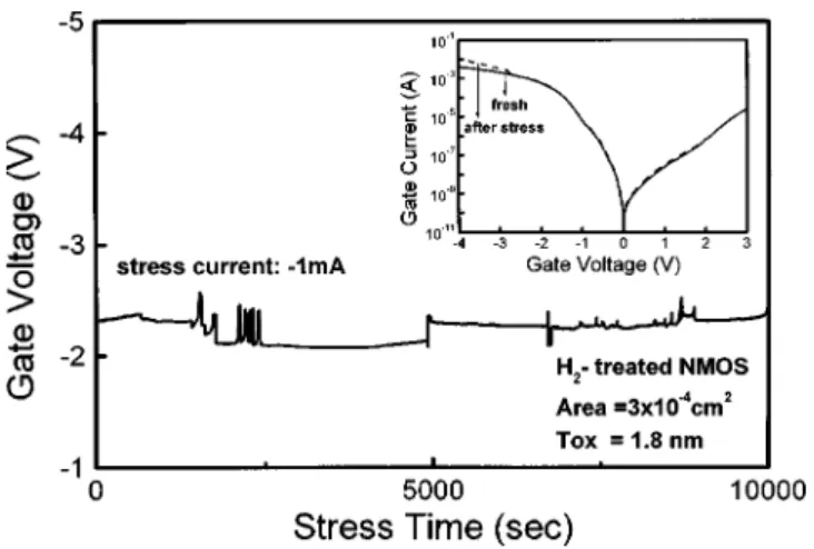
The H2-treated NMOS diodes with thinner oxide
thick-ness共1.8 nm兲 is stressed at high injected current density 共⫺3 A/cm2兲, at least two order of magnitude larger than previous current density, to increase the impact rate of electrons, and the initial gate bias is⫺2.3 V 共Fig. 3兲. The gate bias voltage is plotted as a function of stress time during constant current stress. Though the bias voltage does not exceed the threshold voltage共⫺4 V兲 described previously, the fluctuations in gate voltage under constant current stress and an anomalous in-crease of current in the I – V curve after 10 000 s stress imply that soft breakdown occurs even the gate bias voltage smaller than ⫺4 V. In this case, we propose that the desorption of the Si–H bond is mainly via multiple vibrational excitation by injected electrons within the lifetime of the excited Si–H
bond. This speculative mechanism is also illustrated in Fig. 5共b兲.
In the same stress condition共⫺3 A/cm2兲, the D2-treated
NMOS (tox⫽1.6 nm) diodes reveal the typical isotope ef-fect. There is no apparent fluctuation in gate voltage during stress, and the current–voltage characteristic of device after stress is almost identical to the fresh one共Fig. 4兲. The elec-trons with energy below threshold voltage do not break the Si–D bond despite the high impact rate. Van de Walle and Jackson8 have reported that due to the frequency of Si–D bending mode close to the vibrational frequency of silicon phonon, the lifetime of an excited Si–D bond is shorter than that of an excited Si–H bond. Therefore, it would be difficult to reach a vibrational excited state of a Si–D bond owing to the rapid decay of the Si–D mode.
The lifetime of Si–H/D bonds can be estimated through the previous experimental results, and is given by
impact–rate⬇Jstress/1.6⫻10
⫺19共coul兲
关H兴or关D兴 ,
where Jstress is the stress current density, and 关H兴 共关D兴兲 is the concentration of hydrogen 共deuterium兲 at Si/SiO2
inter-face. The value of关H兴 共关D兴兲 is assumed to be ⬃1013cm⫺2.13
If the lifetime of Si–H/D bonds at excited states exceeds the FIG. 2. The gate voltage vs stress time plot of D2-treated NMOS diodes
under different low current density injection. The inset is the current– voltage characteristics of device before and after⫺50A CCS.
FIG. 3. High current共low initial gate bias兲 stress of H2-treated NMOS. Soft
breakdown occurs after ⬃1000 s stress. The inset is the current–voltage characteristics of device before and after stress.
FIG. 4. High current共low initial gate bias兲 stress of D2-treated NMOS. No
apparent fluctuation in gate voltage is observed. The inset is the current– voltage characteristics of device before and after stress.
638 Appl. Phys. Lett., Vol. 78, No. 5, 29 January 2001 Lin, Lee, and Liu
reciprocal of impact rate, the bonds will be broken by in-jected electrons via multiple vibrational excitation. On the other hand, if the lifetime of excited states is shorter than the reciprocal of impact rate, the Si–H/D bonds will not be bro-ken due to the relaxation to lower-energy states. At lower bias voltage (兩Vg兩⬍4 V), the hydrogen-treated devices
stressed under high current density condition 共⫺3 A/cm2兲 reveal soft breakdown, which is not observed at low stress current density condition (⫺3⫻10⫺3A/cm2). The recipro-cal of impact rates in these two stress conditions are 5 ⫻10⫺7 and 5⫻10⫺4s, respectively, and the lifetime of an excited Si–H bond will lie in between these two values. Soft breakdown does not occur in the D2-treated device under the
current stress as large as ⫺3 A/cm2. This indicates the life-time of an excited Si–D bond is shorter than 5⫻10⫺7s. The excited Si–D bond indeed has a shorter lifetime than that of an excited Si–H bond by the calculation of Foley et al.,14 and the calculated lifetime of excited Si–D bonds is 2 ⫻10⫺10s.
In conclusion, the desorption of Si–H/D bonds are moni-tored by the occurrence of soft breakdown on NMOS diodes under constant current stress. If the bias voltage exceeds
⫺4 V 共the electron energy is ⬃3 eV兲, both the hydrogen and deuterium atoms will emit over the barrier directly by direct electron excitation. Under high current stress condition共high carrier impact rate兲 at low gate voltage, the Si–H bond may be broken via multiple vibrational excitation. However, the isotope effect is observed for D2-treated NMOS due to the
vibration frequency resonance between Si–D bending mode and transverse optical phonon states. The Si–D bond will decay rapidly after excitation by the injected electrons. The speculative mechanisms of excitation are schematically illus-trated in Fig. 5. High-energy electrons can directly excite both hydrogen and deuterium over the barrier 关Fig. 5共a兲兴. Low-energy electrons with high impact rate can desorb the Si–H bond by multiple vibrational excitation, but can rarely desorb the Si–D bond due to the shorter lifetime of the Si–D bond关Fig. 5共b兲兴.
This work is supported by National Science Council, Taiwan, R.O.C. 共Contract No. 89-2218-E-002-017 and No. 89-2218-E-002-012兲 and Yen Tjing-Ling Foundation.
1
S.-H. Lee, B.-J. Cho, J.-C. Kim, and S.-H. Choi, Tech. Dig. Int. Electron Devices Meet. 749,共1994兲.
2M. Depas, T. Nigam, and M. M. Heyns, IEEE Trans. Electron Devices 43,
1499共1996兲.
3B. E. Weir, P. J. Silverman, D. Monroe, K. S. Krisch, M. A. Alam, G. B.
Alers, T. W. Sorsch, G. L. Timp, F. Baumann, C. T. Liu, Y. Ma, and D. Hwang, Tech. Dig. Int. Electron Devices Meet. 73,共1997兲.
4T. Tomita, H. Utsunomiya, T. Sakura, Y. Kamakura, and K. Taniguchi,
IEEE Trans. Electron Devices 46, 159共1999兲.
5
D. J. DiMaria and E. Cartier, J. Appl. Phys. 78, 3883共1995兲.
6
T.-C. Shen, C. Wang, G. C. Abeln, J. R. Tucker, J. W. Lyding, Ph. Avouris, and R. E. Walkup, Science 268, 1590共1995兲.
7J. W. Lyding, K. Hess, and I. C. Kizilyalli, Appl. Phys. Lett. 68, 2526
共1996兲.
8
C. G. Van de Walle and W. B. Jackson, Appl. Phys. Lett. 69, 2441共1996兲.
9R. Biswas, Y.-P. Li, and B. C. Pan, Appl. Phys. Lett. 72, 3500共1998兲. 10K. Hess, I. C. Kizilyalli, and J. W. Lyding, IEEE Trans. Electron Devices
45, 406共1998兲.
11C. G. Van de Walle and R. A. Street, Phys. Rev. B 49, 14 766共1994兲. 12
J. H. Wei, M. S. Sun, and S. C. Lee, Appl. Phys. Lett. 71, 1498共1997兲.
13M. A. Briere and D. Bra¨unig, Trans. Nucl. Sci. 37, 1658共1990兲. 14E. T. Foley, A. F. Kam, J. W. Lyding, and Ph. Avouris, Phys. Rev. Lett.
80, 1336共1998兲.
FIG. 5. Schematic diagrams of the speculative mechanism of Si–H/D bonds desorption.共a兲 The H/D atoms emit over the barrier directly if the initial gate bias exceeds⫺4 V. 共b兲 At low initial gate bias and high current density stress, the giant isotope effect is observed on the D2 sample due to the
relaxation back to low energy states. The hydrogen is up pumping to the transport mobile states via multiple vibrational excitation.
639
Appl. Phys. Lett., Vol. 78, No. 5, 29 January 2001 Lin, Lee, and Liu