Study on Active Touch Sensing Circuit
Implemented by Dual Gate IGZO TFTs
:
:
:
:
Cheng-Che Lee
:
:
:
:
Dr. Ya-Hsiang Tai
Study on Active Touch Sensing Circuit Implemented by
Dual Gate IGZO TFTs
:
Student: Cheng-Che Lee
:
Advisor: Dr. Ya-Hsiang Tai
A Thesis
Submitted to the Display Institute
College of Electrical and Computer Engineering
National Chiao Tung University
in Partial Fulfillment of the Requirements
for the Degree of Master
in
Display Institute
June 2011
Hsinchu, Taiwan, Republic of China
銦IGZO TFT) RC RC IC
Study on Active Touch Sensing Circuit
Implemented by Dual Gate IGZO TFTs
Student
Cheng -Che Lee Advisor
Dr. Ya-Hsiang Tai
Display Institute,
National Chiao Tung University
Abstract
The dual gate IGZO TFT is proposed to be used in an active matrix touch sensing circuit with a RC low-pass filter. Since the dual gate IGZO TFT can be controlled by both its top and bottom gates, only one TFT is needed in the proposed circuit, which enlarges the open ratio of sensing pixel. By a touch event which increases the RC time-constant, a significant transient ON current is generated to be the sensing signal. This signal can be easily read out and thus reduce the cost of peripheral ICs. In addition, this sensor consumes less standby power because no signal current occurs if it is not touched. In such design, it makes considerable improvement over the drawbacks of previous touch sensing technology. Thus, we believe the proposed sensing circuit could be an excellent way to implement active matrix touch panels.
Acknowledgements
: : : : : 2鎵11.鎵6.1鎵Contents
Chinese Abstract ...I
English Abstract ... II
Acknowledgements... III
Contents...IV
Table Captions...VI
Figure Captions ... VII
Chapter 1 Introduction
1.1 Background... 1
1.2 Motivation ... 3
1.3 Thesis Organization ... 4
Chapter 2
Touch Sensing Pixel Circuit
2.1 Direct Touch Sensor Design ... 122.1.1 Sensing Circuit ... 12
2.1.2 Multi-touch Function... 12
2.1.3 Experimental Results... 13
2.2 Indirect Touch Sensor Design... 13
2.2.1 Sensing Circuit Tryout... 13
2.2.2 The Pulse Overlapping Method ... 14
2.2.3 Experimental Results... 15
2.3 Summary... 15
Chapter 3 Stability of the Sensing Pixel Circuit
3.1 Stability Analysis Criteria... 263.1.1 Analysis Base... 26
3.2 Environmental Interference ... 28
3.2.1 Temperature Effect ... 28
3.2.2 Illumination Effect... 29
3.3 Electrical Stress Stability... 30
3.3.1 DC stress... 30
3.3.2 AC stress ... 31
3.4 Summary... 31
Chapter 4 Conclusions & Future Works
... 45Table Captions
Chapter 3
Table 3-1 Measurement conditions for the temperature effect ... 35
Table 3-2 Measurement conditions for the illumination effect ... 38
Table 3-3 Experiment conditions of DC stress. ... 41
Figure Captions
Chapter 1
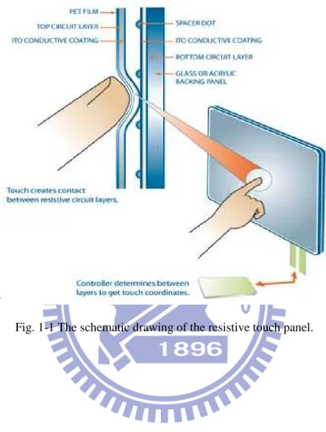
Fig. 1-1 The schematic drawing of the resistive touch panel. ... 6
Fig. 1-2 (a) The sketch map of PCTP operation principle with panel is untouched... 7
Fig. 1-2 (b) The sketch map of PCTP operation principle with panel is touched. ... 7
Fig. 1-3 The touch position determination of PCTP. ... 7
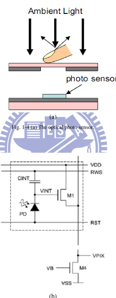
Fig. 1-4 (a) The optical photo sensor. ... 8
Fig. 1-4 (b) The equivalent circuit of sensor pixel with photo diode. ... 8
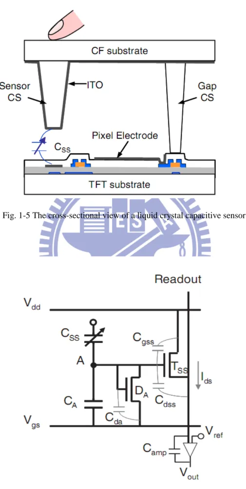
Fig. 1-5 The cross-sectional view of a liquid crystal capacitive sensor. ... 9
Fig. 1-6 The equivalent circuit for liquid crystal capacitance detector... 9
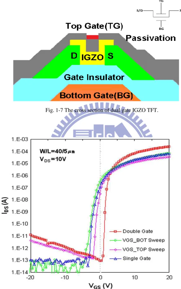
Fig. 1-7 The cross section of dual gate IGZO TFT... 10
Fig. 1-8 The transfer characteristics of the dual gate TFT. [ IEEE Electron Devices Letter, Vol. 31, no. 3, pp. 219-221, 2010 ] ... 10
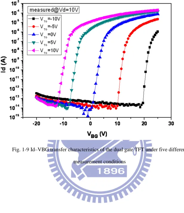
Fig. 1-9 Id–VBG transfer characteristics of the dual gate TFT under five different measurement conditions ... 11
Chapter 2
Fig. 2-1(a) The schematic of sensing circuit using dual gate TFT at the bias condition of (VBG, Vd, Vs) = (-15V.-5V,-15V). ... 17Fig. 2-1(b) The transient current experimental result for touch detection... 17
Fig. 2-2(a) The schematic of sensing circuit using dual gate TFT at the bias condition of (VBG, VTG, Vd, Vs) = (-15V.-5V.-5V,-15V). ... 18
Fig. 2-2(b) The improved transient current experimental result for touch detection. ... 18
Fig. 2-3 The characteristics of a dual gate IGZO TFT at different VTG conditions... 19
Fig. 2-4 The designed timing diagram and four cases of the multi-touch... 19
Fig. 2-6 The multi-touch experimental results. ... 20
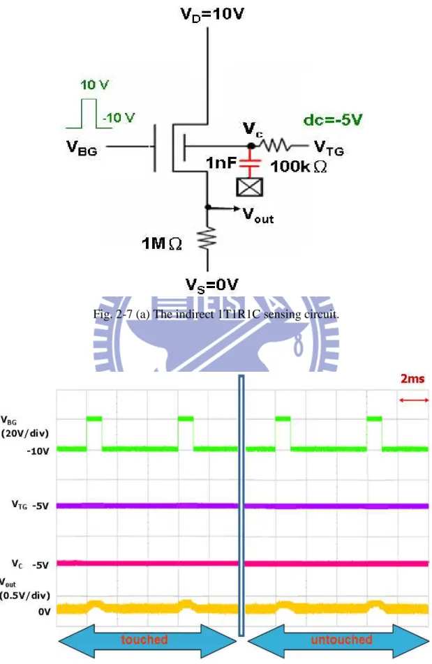
Fig. 2-7 (a) The indirect 1T1R1C sensing circuit... 21
Fig. 2-7 (b) The first tryout result... 21
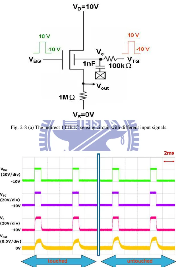
Fig. 2-8 (a) The indirect 1T1R1C sensing circuit with different input signals... 22
Fig. 2-8 (b) The second tryout result. ... 22
Fig. 2-9 The waveforms at bottom gate (VBG) and node C (VC) of the second tryout result. .. 23
Fig. 2-10 The designed timing diagram of pulse overlapping method... 23
Fig. 2-11 The transfer characteristics of the dual gate IGZO TFT (a) sweeping VTG = VBG (b) VTG = -10V, sweeping VBG and (c) VBG = -10V, sweeping VTG... 24
Fig. 2-12 (a) The indirect 1T1R1C sensing circuit with the designed input signals. ... 25
Fig. 2-12 (b) The measurement result of indirect touch operation. ... 25
Chapter 3
Fig. 3-1 The timing diagram of the top and bottom gate voltage pulses in the two cases of misjudgment for touch event. ... 33Fig. 3-2 The transfer characteristics for the dual gate TFT at the VTG =-2V. It also shows the judging criteria for touch case. ... 34
Fig. 3-3 The transfer characteristics for the dual gate TFT at the VTG =-10V. It also shows the judging criteria for untouched case. ... 34
Fig. 3-4 The transfer characteristics at different temperatures for the dual gate TFT. ... 35
Fig. 3-5 The temperature dependencies of threshold voltage (Vth) shift and mobility ratio. .. 36
Fig. 3-6 The diagram of applying judging criteria to evaluate the temperature working range. ... 36
Fig. 3-7 The measurement result of sensing circuit at 75 degrees. ... 37
Fig. 3-8 The measurement result of sensing circuit at 85 degrees. ... 37
Fig. 3-9 The transfer characteristics at different illumination intensity for the dual gate TFT. ... 38
Fig. 3-10 The illumination intensity dependencies of threshold voltage (Vth) shift and
mobility ratio. ... 39 Fig. 3-11 The diagram of applying judging criteria to evaluate the illuminance working range. ... 39 Fig. 3-12 The measurement result of sensing circuit under 1006 lux. ... 40 Fig. 3-13 The measurement result of sensing circuit under 1500 lux. ... 40 Fig. 3-14 The evolution of dual gate IGZO TFT transfer characteristics at the stress condition (VTG,VBG) = (10V,-10V). The inset shows the evolution of transfer curves at stress
condition (VTG,VBG) = (-10V,10V). ... 41
Fig. 3-15 The evolution of dual gate IGZO TFT transfer characteristics at the stress condition (VTG,VBG) = (-10V,-10V)... 42
Fig. 3-16 The waveform of gate pulse signal during AC stress experiment. ... 43 Fig. 3-17 The evolution of dual gate IGZO TFT transfer characteristics under AC stress. ... 44 Fig. 3-18 The threshold voltage (Vth) shift versus effective stress time for AC stress. The inset illustrates the pulse waveform for AC experiment. ... 44
Chapter 1
Introduction
1.1 Background
1.1.1 Touch panel
Touch panel (TP) has attracted much attention in various applications since it is easy to use and does not need any additional input devices such as keyboards or mice. For this reason, touch panel has been widely applied to many products, such as personal digital assistants, hand-held phones, digital camera, and tablet PCs. Therefore, the touch panel market is growing up in incredible speed.
Touch panel mainly divided into two categories. One is passive matrix TP, and the other is active matrix TP. For passive matrix TP, the earliest touch panel is resistive type, which uses two ITO films biased and dot spacers holding the structure between them.Fig. 1-1 shows the structure and operation of resistive touch panel. When touching, the pressure of the external force makes the upper ITO layer contact with the lower ITO and the voltage drop at that touching point becomes zero. Consequently, the touching input function can be realized by recognizing the site of the short circuit. Although the resistive touch panel operation is simple, the physical abrasion and lower photo penetration can scarcely be accepted.
Besides the resistive touch panel, Projective Capacitive Touch Panel (PCTP) is adapted. The PCTP has higher sensitivity and the sketch map of its operation principle is shown in Fig. 1-2. Unlike the resistive touch panel, it does not need any external force. The touch position information is determined from the change of capacitive value when human’s hands touch on the panel, which is shown in Fig 1-3. But, there are two drawbacks of PCTP. One is that the readout IC must be very sensitive, because the change of capacitive value is small, which
makes the IC high cost. Another drawback in PCTP is that, when panel size becomes large, touch signal is hardly to be read by IC.
It turns out to be that active matrix is an effective solution to achieve a large size TP. There are two major technologies to achieve active matrix TP; one of them is optical sensor, which is shown in Fig. 1-4 [1]. The equivalent circuit consists of a photo diode (PD) and one amplifier (M1). This optical sensor works by detecting the difference of current due to light intensity between touch and untouched states. However the sensing method makes it difficult to use since the sensor is apt to respond to unintended light noise.
Another approach for active TP is Liquid-Crystal Capacitance (LCC) Detector. The capacitive touch sensor which is composed of a liquid crystal capacitor and sensing transistors. Fig. 1-5 and Fig. 1-6show the cross-sectional view of a capacitive sensor and the equivalent circuit [2]. The capacitive sensor is fabricated on a TFT substrate and a color filter substrate. And liquid crystal is used to fill the space between them. When a touch event occurs, there is a slight reduction in cell gap and the capacitance of Css increases, thus voltage at node A in Fig. 1-6 decreases. For this reason, the drain current Id becomes smaller when sensor is touched. The output current signal is different when sensor is touched or untouched. Therefore, we can detect a touch event from the output voltage (Vout) change.
However, Liquid-Crystal Capacitance Detector has two disadvantages. One is that, because the transistor Tss is always on, it always consumes power whether pixel is touched or not. The other disadvantage is that, when the electrical instability in sensing transistors occurs, touch signal and untouched signal in different pixels are difficultly distinguished by the same readout circuit. For this reason, we try to propose a new sensing method to detect touch events.
1.1.2 Thin film transistor
proposed. Fig.1-7 shows the schematic cross section of dual gate IGZO TFT and circuit symbol of the device in the inset. Compared to conventional single-gate IGZO TFT, the difference is the top gate layer made by ITO deposited upon the passivation layer. From previous reference, the electrical characteristics of dual gate IGZO TFT are greatly improved with respect to the conventional single-gate IGZO TFT, which is shown in Fig. 1-8 [3-4]. In addition, we also investigated the I–V characteristics of the dual gate IGZO TFT with different bias voltages applied to each gate. Fig.1-9 shows the transfer curves of drain current (Id) versus bottom-gate voltage (VBG) for the dual gate IGZO TFT at different top-gate
voltages (VTG). These transfer curves exhibit parallel shifts with respect to different VTG
values. This phenomenon is attributed to attraction and expelling of free carriers in the active layer by the top-gate. It implies that, the threshold voltage of the dual gate IGZO TFT using the bottom-gate in its normal operation can be controlled by the top-gate and vice versa. This gives us an idea of using it for the touch sensor application.
1.2 Motivation
In this thesis, we attempt to develop an active matrix touch sensing circuit implemented by dual gate IGZO TFT. Our notion is that, once a touch event occurs, the dual gate IGZO TFT will switch from off to turned on state. In such a case, a significant transient ON current flows through the TFT to be the sensing signal. Thus we can easily read out the current signal and detect touch events. In such a way, the touch sensing circuit has some advantages. One of them is that dual gate IGZO TFT has better device performance, such as high mobility, high on/off ratio and excellent uniformity, which can provide larger aperture for the pixels. Moreover, the touch sensing circuit uses the output current as the sensing signal to avoid the effect of the bus capacitance. As a result, the proposed touch sensing circuit may be an effective solution to achieve a large size TP.
The designed touch sensing circuit expects to achieve following properties: (1) Power consumption is curtailed when a pixel is untouched.
(2) Signal can be read easily when a pixel is touched.
1.3 Thesis Organization
In chapter 2, the implementation of the touch sensing circuit is described. The designed circuit only uses one dual gate IGZO TFT as sensing transistor with reduced circuit complexity. Then, in order to examine the reliability of designed circuit, we compare the operating regions of dual gate IGZO TFT in the following chapter. The environmental interference of the dual gate IGZO TFT for both temperature and illumination intensity are intensively analyzed in chapter 3, along with the comparison of circuit stability under electrical stress. Finally, in chapter 4, the conclusion of the feasibility to realize the touch panel with dual gate IGZO TFT is given.
The section organization of this thesis is listed below:
Chapter 1: Introduction
1.1 Background
1.2 Motivation
1.3 Thesis Organization
Chapter 2: Touch Sensing Pixel Circuit
2.1 Direct Touch Sensor Design
2.1.1 Sensing Circuit
2.1.2 Multi-touch Function
2.1.3 Experimental Results
2.2 Indirect Touch Sensor Design
2.2.1 Sensing Circuit Tryout
2.2.2 The Pulse Overlapping Method
2.2.3 Experimental Results
2.3 Summary
Chapter 3: Stability of the Sensing Pixel Circuit
3.1 Stability Analysis Criteria
3.1.1 Analysis Base
3.1.2 Working Range Evaluation
3.2 Environmental Interferences
3.2.1 Temperature Effect
3.2.2 Illumination Effect
3.3 Electrical Stress Stability
3.3.1 DC stress
3.3.2 AC stress
3.4 Summary
Chapter 4: Conclusions & Future Works
References
`
Fig. 1-2 (a) The sketch map of PCTP operation principle with panel is untouched.
(b)
Fig. 1-2 (b) The sketch map of PCTP operation principle with panel is touched.
(a)
Fig. 1-4 (a) The optical photo sensor.
(b)
Fig. 1-5 The cross-sectional view of a liquid crystal capacitive sensor.
Fig. 1-7 The cross section of dual gate IGZO TFT.
Fig. 1-8 The transfer characteristics of the dual gate TFT. [ IEEE Electron Devices Letter, Vol. 31, no. 3, pp. 219-221, 2010 ]
Fig. 1-9 Id–VBG transfer characteristics of the dual gate TFT under five different measurement conditions
Chapter 2
Touch Sensing Pixel Circuit
2.1 Direct Touch Sensor Design
2.1.1 Sensing Circuit
Fig. 2-1(a) shows the schematic of the proposed sensing circuit using dual gate IGZO TFT and its bias condition. We choose top-gate as the sensing pad and keep TFT in off state initially. Here, we assume that the top gate touched with hand is as good as ground. When a touch event occurs, the sensing TFT will switch from off to turned on state. In such a case, a significant transient ON current flows through the TFT to be the sensing signal. Fig. 2-1(b) shows the TFT transient current measurement result of touch detection. The result verifies our preliminary idea, when a touch event occurs to produce significant transient ON current.
However, this design has a drawback of slow response time when the state of top-gate changes from touched to floating. In order to improve this case, we attempt to set a path on top-gate for pulling back the voltage back to a preset bias. Fig. 2-2 shows the schematic of sensing circuit with the bias condition and the measurement result. We add a resistance in the circuit to reduce the leakage current. The experimental result conforms that as the touch is released, the voltage is pulled back to the voltage bias quickly. Thus, the response time is improved. We indeed prove that the dual gate IGZO TFT can be used for touch sensor.
2.1.2 Multi-touch Function
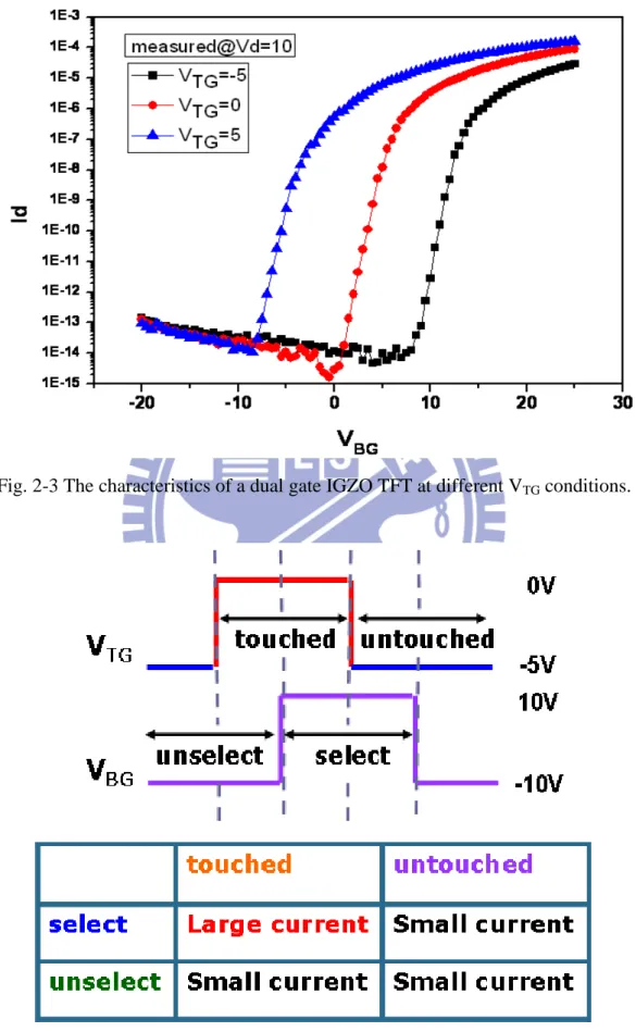
The proposed touch sensing method can achieve multi-touch function. Fig. 2-3 illustrates the characteristics of a dual gate IGZO TFT at different VTG conditions. For most of the time,
touch event happens, the top-gate voltage change makes TFT turned on. For such a concept, the timing diagram is shown in Fig. 2-4. There are four cases of the multi-touch operation. The significant output current signal occurs only when the sensing circuit is selected and touched simultaneously. In other cases, the output current signal is very small. Thus, this circuit can support multi-touch function.
2.1.3 Experimental Results
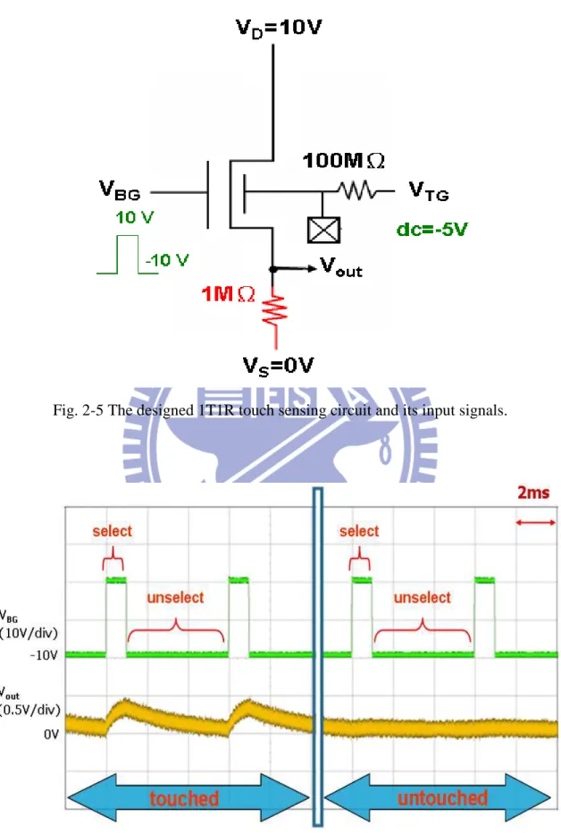
Fig. 2-5 shows the designed 1T1R touch sensing circuit and its input signals. The design target is that the touch signal should be larger than the untouched signal for 0.2V, which can be easily distinguished by readout ICs. Fig. 2-6 shows the multi-touch experimental results. In order to prove the easiness of reading out the sensing current, we simply used a resistor of 1Mohm to measure the transient current. It is clearly seen that the difference between output signals for the two cases is obvious. The proposed sensing circuit undoubtedly supports multi-touch function.
However, the direct touch operation is hardly used in general applications because the panel is usually covered by a protection layer. Accordingly, the indirect touch operation needs to be considered.
2.2 Indirect Touch Sensor Design
2.2.1 Sensing Circuit Tryout
In applications, the indirect touch operation is more extensively used. Thus, we attempt to add a capacitance in the touch sensing circuit to model the indirect touch on the sensing pad through the protection layer. Fig. 2-7 (a) shows the first version of the indirect touch sensing circuit using 1 TFT, 1 resistor, and 1 capacitor. In the first tryout measurement, the same input signals as those for the direct touch operation are applied disregarding of the sensing
capacitance. In this tryout, the resistance is 100kohm, the sensing capacitance is 1nF, and the same 1Mohm resistance is used to be a readout indicator. As shown in Fig.2.7 (b), the voltage at node C is fixed at VTG no matter it is touched or not. The voltage waveform (Vout) on the
readout resistor is indistinguishable. The tryout sensing circuit does not work owing to the DC blocking of the capacitor. In order to fix this problem, the top-gate voltage is changed to AC signal. Fig. 2-8 shows the second sensing circuit tryout with different input signals and its result. The output waveforms are different in response to the touch. However, similar to the Liquid-Crystal Capacitance Detector, the second tryout has the disadvantage of high standby power consumption. Therefore, a new method is expected to detect touch events.
2.2.2 The Pulse Overlapping Method
The waveforms at bottom gate (VBG) and node C (VC) of the second tryout result are
observed in more detail. The waveform at node C is the voltage at the top gate after RC time delay. As shown in Fig. 2-9, the waveform at node C exhibits different waveform distortions for the two cases. When a touch event occurs, the larger RC delay leads to more serious pulse distortion. It prolongs the voltage falling time of VTG. Thus, this gives us an idea of using it
for the indirect touch operation.
Fig. 2-10 shows the concept of pulse overlapping inspired by the waveform distortion. The input signal at bottom gate is modified by shifting its phase in time. In order to confirm the low power consumption at the operational states of unselected and untouched of this design, the characteristics of the dual gate TFT with respect to either top or bottom gate bias are checked. As illustrated in Fig. 2-11, the TFT is kept OFF by biasing VTG at -10V even when
the VBG is as high as +10V, and vice versa. Thus, this design indeed could reduce power
consumption of standby.
of the time, both the top and bottom gates of the dual gate TFT are set at -10V and the TFT is turned off. Just before the VBG pulse coming to the bottom gate, the pulse of VTG is sent to the
top gate through the RC circuit. If no touch event occurs at this time, the RC time delay is small. Thus, the slightly distorted VTG pulse can fall in time to -10V to turn off the TFT before
the VBG comes in. On the other hand, if a touch event happens, it results in large RC time
delay. The larger RC delay leads to more serious pulse distortion and prolongs the voltage falling time of VTG. This delay time keeps the TFT from turning off by the time that the
bottom-gate switches to +10V. In such a case, a significant transient ON current flows through the TFT to be the sensing signal. Consequently, we can use the method to detect touch events.
2.2.3
Experimental Results
Fig. 2-12 shows the schematic of 1T1R1C sensing circuit with the input signals and its measurement result. For the touched case, VA is high and VC is not low enough to turn off the
TFT. The spikes in the output voltage waveform (Vout) on the readout resistor indicate the
touch events. In other words, when touch event occurs, it results in a significant transient current. On the other hand, for the untouched case, no current is observed. It implies that the proposed sensing method does not consume readout power when sensing circuit is not touched. The power consumption of the circuit is greatly reduced. Thus, we indeed think the pulse overlapping method is an effective solution to detect touch events.
2.3 Summary
We have verified the feasibility of the proposed sensing circuit. For indirect touch operation, we use the pulse overlapping method to detect touch events. The operation uses the significant transient ON current as the sensing signal. This signal can be easily read out by low cost ICs. Moreover, the proposed sensing circuit consumes low standby power. Thus, the proposed
design may be an excellent way to implement active matrix touch panels.
However, the TFT is subject to the issues of uniformity, reliability, and the influence of the environment. The device characteristics may be not stable and neither be the performance of sensing circuit. Thus, in chapter 3, we will investigate the stability of the proposed sensing circuit for the practical applications.
Fig. 2-1(a) The schematic of sensing circuit using dual gate TFT at the bias condition of (VBG,
Vd, Vs) = (-15V.-5V,-15V).
Fig. 2-2(a) The schematic of sensing circuit using dual gate TFT at the bias condition of (VBG,
VTG, Vd, Vs) = (-15V.-5V.-5V,-15V).
Fig. 2-3 The characteristics of a dual gate IGZO TFT at different VTG conditions.
Fig. 2-5 The designed 1T1R touch sensing circuit and its input signals.
Fig. 2-7 (a) The indirect 1T1R1C sensing circuit.
Fig. 2-8 (a) The indirect 1T1R1C sensing circuit with different input signals.
Fig. 2-9The waveforms at bottom gate (VBG) and node C (VC) of the second tryout result.
Fig. 2-11 The transfer characteristics of the dual gate IGZO TFT (a) sweeping VTG = VBG (b) VTG = -10V, sweeping VBG and (c) VBG = -10V, sweeping VTG.
Fig. 2-12 (a) The indirect 1T1R1C sensing circuit with the designed input signals.
Chapter 3
Stability of the Sensing Pixel Circuit
In the proposed sensing pixel circuit, only one dual gate IGZO TFT is used. The dual gate IGZO TFT has better device performance, but it still has some problems such as the threshold voltage (Vth) shift and unsatisfactory stability [5-8]. The device characteristics may be not stable and neither be the performance of sensing circuit. Thus, it is essential to evaluate the stability of the sensing circuit for the practical applications.
3.1 Stability Analysis Criteria
3.1.1 Analysis Base
Fig. 3-1 shows the timing diagram of the top and bottom gate voltage pulses in the touch and untouched cases. For the touch case, the distorted VTG pulse crosses over VBG pulse at
point P. At this time, the VBG and VTG at point P are 10V and -2V, respectively. In such case, a
significant transient ON current flows through the TFT to be the sensing signal.On the other hand, for the case of untouched, the VBG and VTG at the sensing moment are 10V and -10V
respectively. The output current is too small to be determined. Thus, the sensing circuit can properly detect touch events
However, if the Vth variation of dual gate TFT occurs, it will lead to misjudgments. Consequently, we need to propose a method to evaluate the working range of the sensing circuit.
3.1.2 Working Range Evaluation
Since the sensing pixel circuit simply consists of one transistor, the limits of Vth shift can be acquired by analyzing the device characteristics of the dual gate IGZO TFT. Based on this concept, we propose the analysis criteria to evaluate the working range of the sensing circuit.
For the touch case, the output current signal should be larger than 200nA to create a voltage difference of 0.2V on the readout resistance for touch judgment. It can be used as our judging criteria for touch events. Fig. 3-2 shows the transfer characteristics for the dual gate TFT at the top gate bias condition of -2V. We plot a horizontal line for the output current signal of 200nA. If Vth of the sensing transistor shifts negatively, the corresponding output current at VBG of 10V is surely larger than 200nA. However, if Vth shifts to too positive, the
corresponding output current will be smaller than 200nA. In such case, the misjudgment of touch events occurred. Thus, there is a positive limit of Vth shift for the touch case.
On the other hand, for the untouched case, the output current signal should be smaller than certain current level, for example tenth of 200nA. This value is used as our judging criteria for untouched events. Fig. 3-3 shows the transfer characteristics for the dual gate TFT at the top gate bias condition of -10V. We plot a horizontal line for the output current signal of 20nA. The normal output current is always smaller than 20nA. However, if Vth of the sensing transistor shifts to too negative, the unwanted output current signal is generated, leading to the misjudgment. Thus, there is a negative limit of Vth shift for the untouched case.
The two cases of misjudgment for touch event are indicated by the dash lines in Fig. 3-1. By analyzing Vth shift of the transistor, we can estimate the working range of sensing circuit. The proposed analysis criteria are effective methods for the sensing circuit stability investigation.
3.2 Environmental Interference
Many studies have proposed that the environmental interferences may affect the stability of the dual gate TFT. Among them, the temperature and illumination influences are significant. Thus, we need to evaluate the working range of the sensing circuit under environmental interference.
3.2.1 Temperature Effect
Table 3-1 lists the experiment conditions for temperature effect. The dual gate TFT is measured at different temperatures of 25 to 85 oC. Fig. 3-4 shows the transfer characteristics of the TFT at different temperatures. The clear trend is that the Vth decreases with increasing temperature. In previous reports, it can be attributed to the free electrons generated along with the oxygen vacancies during increasing temperature [9-11]. The temperature dependence of mobility ratio is shown in Fig. 3-5. It also verifies the carrier detrapping at higher temperatures. Thus, the operating temperature obviously affects the stability of the dual gate TFT.
As just mentioned, the transfer curve is shifted in negative direction with incrementing temperature. It implies that the increasing temperature will lead to misjudgment of the untouched case. Therefore, we need to evaluate the temperature tolerance range of the sensing circuit.
As shown in Fig. 3-6, we plot a horizontal line for the judging criteria of 20nA. Then, we plot a vertical line at VBG of 10V. The maximum operating temperature of the sensing circuit
can be estimated from the figure. For our device, the curve of 85 oC is on the negative side of the cross point, while the curve of 75 oC is on the positive side. It implies that the maximum operationg temperature is about 80 degrees. To verify this limit extracted from the device characteristics, the sensing circuit performances at different temperatures are measured.
Fig. 3-7 and Fig. 3-8 show the measurement results of the sensing circuit at different temperatures. The sensing circuit still works correctly even at 75 oC. However, when the operating temperature is up to 85 oC, the spikes occur in the output voltage waveform (Vout) no matter the pixel is touched or not. It may lead to the misjudgment when the circuit is operated at 85 degrees. From these results, it confirms that the proposed sensing circuit has high tolerance of temperature.
3.2.2 Illumination Effect
Table 3-2 lists the experiment conditions for illumination effect. The dual gate TFT is measured at different illumination intensity of 0 lux to 1980 lux. Fig. 3-9 shows the transfer characteristics at different illumination intensities. The Vth shift of the TFT as a function of light intensity is shown in Fig. 3-10. From these results, we observe that the Vth decreases with increasing illumination intensity. This phenomenon could be attributed to the electron detrapping process under light illumination [12-15]. Thus, the increasing light intensity can lead to misjudgment of the untouched case. We need to evaluate the illuminance tolerance range of the sensing circuit.
As shown in Fig. 3-11, we apply the proposed criteria to estimate the maximum operating light intensity of sensing circuit. In our design, the high limit of illumination is about 1300 lux. Then, experiments of the circuit are conducted for verification. Fig. 3-12 and Fig. 3-13 show the measurement results of the sensing circuit under different illumination intensity. When the illumination intensity is up to 1500 lux, the unwanted output signal occurs, while the sensing circuit still works correctly at 1006 lux. Thus, the proposed sensing circuit also has high tolerance of illumination intensity.
Again, the experimental results verify the validity of the proposed judging criteria based on device characteristics. In other words, the working range of the sensing circuit can be
evaluated directly by analyzing the characteristics of the dual gate TFT. Thus, the analysis criteria could be applied for the stress stability investigation.
3.3 Electrical Stress Stability
Except for the environmental interferences, the electrical stress also affects the stability of dual gate IGZO TFT. In order to examine the stability of the sensing circuit, various experiments for DC and AC stress were performed. We use a fresh TFT sample for each stress condition to ensure the uniformity of initial characteristics.
3.3.1 DC stress
Table 3-3 lists the DC stress conditions that we designed for the instability test of the TFT. These stress conditions correspond to different steady states of touch sensing operation. Fig. 3-14 and Fig. 3-15 show the evolution of dual gate TFT transfer characteristics at different stress conditions. In the measurement process, both gates of the TFT are tied together.
From the results, it can be seen that the transfer characteristics of the TFT before and after the bias stress have a similar shape except for a parallel shift. The transfer curves are shifted in the positive direction by incrementing the positive VBG stress time. On the other hand,
when the TFT isstressed at the negative VBG, Vth is shifted in the negative direction. Many
researchers speculate that the parallel shift may be caused by carrier trapping into the gate dielectric and at the interface between the gate dielectric and the active layer [16-18]. The phenomenon of Vth parallel shift may affect the stability of sensing circuit.
The fast degradation of the devices under DC stress at VBG=-10V and VTG=10V seems to
obstruct the application. However, in our design, we use the pulsed input signal for the sensing circuit. The dual gate TFT is usually operated under the AC signals rather than DC biases. Thus, it is more crucial to investigate the stability of dual gate TFT under AC bias stress.
3.3.2 AC stress
To study the stability of the sensing circuit under AC stress, the periodic pulse signal was applied to the dual gate TFT during the experiment. Fig. 3-16 illustrates the waveform of gate pulse signal. The pulse period (PD) and pulse width (PW) are 16ms and 1ms respectively. Moreover, the pulse signal has a base line of -10V and the pulse amplitude of 20V. This condition is more severe than our input signals of the sensing circuit.
Table 3-2 lists the AC stress conditions that we set for investigating the stability of the TFT. In the AC stress experiment, pulse voltage is applied to each gate and the effective stress time is 1500s. Fig. 3-17 shows the evolution of transfer characteristics under AC stress. It can be seen that the transfer curves nearly overlap with each other. This is an indication that the dual gate TFT hardly degrades with time under AC stress.
Fig. 3-18 shows the time dependence of the Vth shift for dual gate TFT under AC stress. A huge reduction of Vth shift is observed for the testing result. This result verifies that the TFT is more stable under AC stress. The phenomenon agrees with previous reports [19-20]. Moreover, we use extrapolation to estimate the lifetime of sensing circuit. After 109 seconds of AC stress, the Vth shift is smaller than 3V. Thus, we think that the lifetime of sensing circuit would be more than 109 seconds. The proposed sensing circuit is robust under the AC operation.
.
3.4 Summary
We have verified the stability of the proposed sensing circuit. By analyzing the device characteristics of the dual gate IGZO TFT, we could evaluate the working range of the circuit. Moreover, from above experimental results, we also confirm the good correspondence between the analysis of the single device and sensing circuit. The sensing circuit is proved to
have high tolerance of bias stress and environmental conditions, which makes it an excellent way to implement active matrix touch panels.
Fig. 3-1 The timing diagram of the top and bottom gate voltage pulses in the two cases of misjudgment for touch event.
Fig. 3-2 The transfer characteristics for the dual gate TFT at the VTG =-2V. It also shows the
judging criteria for touch case.
Fig. 3-3 The transfer characteristics for the dual gate TFT at the VTG =-10V. It also shows the
Table 3-1 Measurement conditions for the temperature effect
Fig. 3-5 The temperature dependencies of threshold voltage (Vth) shift and mobility ratio.
Fig. 3-7 The measurement result of sensing circuit at 75 degrees.
Table 3-2 Measurement conditions for the illumination effect
Fig. 3-10 The illumination intensity dependencies of threshold voltage (Vth) shift and mobility ratio.
Fig. 3-12 The measurement result of sensing circuit under 1006 lux.
Table 3-3 Experiment conditions of DC stress.
Fig. 3-14 The evolution of dual gate IGZO TFT transfer characteristics at the stress condition (VTG,VBG) = (10V,-10V). The inset shows the evolution of transfer curves at stress condition
Fig. 3-15 The evolution of dual gate IGZO TFT transfer characteristics at the stress condition (VTG,VBG) = (-10V,-10V).
Fig. 3-16 The waveform of gate pulse signal during AC stress experiment.
Fig. 3-17 The evolution of dual gate IGZO TFT transfer characteristics under AC stress.
Fig. 3-18 The threshold voltage (Vth) shift versus effective stress time for AC stress. The inset illustrates the pulse waveform for AC experiment.
Chapter 4
Conclusions & Future Works
In this thesis, the touch sensing circuits using dual gate IGZO TFT are proposed. We have verified the feasibility of the proposed sensing circuits. Particularly, for indirect touch operation, we use the pulse overlapping method to detect touch events. The proposed sensing circuit has many advantages. Firstly, the circuit uses the transient ON current as the sensing signal. This current signal only occurs when the sensing pixel is selected and touched at the same time. Therefore, the design consumes low standby power. Secondly, the non-uniformity of the dual gate TFT only varies the current level but not the response time that carries the information of touch. Thirdly, the sensing circuit occupies small area, since only one TFT is used and the two required scan pulses are the same as those in AMLCD. In addition, the circuit supports multi-touch. Thus,the proposed sensing circuit provides an excellent way of implementing large area active matrix touch panels.
Furthermore, we also have verified the stability of the proposed sensing circuit. By analyzing the device characteristics of the dual gate IGZO TFT, we could evaluate the working range of the circuit. The sensing circuit is proven to have high tolerance of bias stress and environmental interferences, which makes the circuit robust in applications.
In the future, we expect the touch sensing circuit could be demonstrated in a prototype panel. Moreover, we also focus on the process optimization of the dual gate IGZO TFT. Thus, it can be an effective solution to achieve the high quality of the active matrix touch panel.
References
[1] Bong Hyun You, Byoung Jun Lee, Jae Hoon Lee, “LCD embedded hybrid touch screen panel”, SID Symposium Digest of Technical Papers, Vol. 40, Issue 1, pp. 439-442, 2009
[2] Cheol Se Kim, Byung Koo Kang, Ji Hyun Jung, “Active matrix touch sensor perceiving liquid crystal capacitance with amorphous silicon thin film transistors”, Japanese Journal of
Applied Physics, Vol. 49, Issue 3, pp. 03CC03, 2010
[3] Kyoung Seok Son, Ji Sim Jung, Kwang Hee Lee, “Characteristics of double-gate GaInZnO thin-film transistor”, IEEE Electron Devices Letter, Vol. 31, no. 3, pp. 219-221, 2010
[4] Kyoung Seok Son, Ji Sim Jung, Kwang Hee Lee, “Highly stable double-gate GaInZnO thin-film transistor”, IEEE Electron Devices Letter, Vol. 31, no. 8, pp. 812-814, 2010
[5] Jae Kyeong Jeong, Hui Won Yang, Jong Han Jeong, “Origin of threshold voltage instability in indium gallium zinc oxide thin film transistors”, Appl. Phys. Letter, Vol. 93, pp.123508, 2008
[6] Jaeseob Lee, Jin Seong Park, Young Shin Pyo, “The influence of the gate dielectrics on threshold voltage instability in amorphous indium gallium zinc oxide thin film transistors”,
Appl. Phys. Letter, Vol. 95, pp.123502, 2009
[7]Donghun Kang, Hyuck Lim, Changjung Kim, “Amorphous gallium indium zinc oxide thin film transistors: sensitive to oxygen molecules”, Appl. Phys. Letter, Vol. 90, pp.192101, 2007. [8] Kenji Nomura, Toshio Kamiya, Masahiro Hirano, “Origins of threshold voltage shifts in room temperature deposited and annealed InGaZnO thin film transistors”, Appl. Phys. Letter , Vol. 95, pp.013502, 2009
[9] Ken Hoshino, John Wager, “Operating temperature trends in amorphous InGaZnO thin-film transistors”, IEEE Electron Devices Letter, Vol. 31, no. 8, pp. 818-820, 2010
[10] Kazushige Takechi, Mitsuru Nakata, Toshimasa Eguchi, “Temperature dependent transfer characteristics of amorphous InGaZnO4 thin film transistors”, Japanese Journal of Applied
Physics, Vol. 48, Issue 1, pp.011301, 2009
[11] Hiromichi Godo, Daisuke Kawae, Shuhei Yoshitomi, “Temperature dependence of transistor characteristics and electronic structure for amorphous In-Ga-Zn-Oxide thin film transistor”, Japanese Journal of Applied Physics, Vol. 49, Issue 3, pp. 03CB04, 2010
[12] Te Chih Chen, Ting Chang Chang, Chih Tsung Tsai, “Behaviors of InGaZnO thin film transistor under illuminated positive gate-bias stress”, Appl. Phys. Letter, Vol. 97, pp. 112104, 2010
[13] Dharam Pal Gosain, Tsutomu Tanaka, “Instability of amorphous indium gallium zinc oxide thin film transistors under light illumination”, Japanese Journal of Applied Physics, Vol. 48, pp. 03B018, 2009
[14] Md Delwar Hossain Chowdhury, Piero Migliorato, Jin Jang, “Light induced instabilities in amorphous indium gallium zinc oxide thin film transistors”, Appl. Phys. Letter, Vol. 97, pp.173506, 2010
[15] Himchan Oh, Sung Min Yoon, Min Ki Ryu, “Photon-accelerated negative bias instability involving subgap states creation in amorphous InGaZnO thin film transistor”, Appl. Phys.
Letter, Vol. 97, pp.183502, 2010
[16] Arun Suresh, John. Muth, “Bias stress stability of indium gallium zinc oxide channel based transparent thin film transistors”, Appl. Phys. Letter, Vol. 92, pp. 033502, 2008
[17] Jeong Min Lee, In Tak Cho, Jong Ho Lee, “Bias stress induced stretched exponential time dependence of threshold voltage shift in InGaZnO thin film transistors ”, Appl. Phys.
Letter , Vol. 93, pp. 093504 , 2009
[18] Edward Namkyu, Cho Jung Han Kang, Chang Eun Kim, “Analysis of bias stress instability in amorphous InGaZnO thin-film transistors”, IEEE Device and Materials Reliability Journal, Vol. 11, Issue 1, pp. 112-117, 2011
[19] Sangwon Lee, Kichan Jeon, Jun Hyun Park, “Electrical stress induced instability of amorphous indium-gallium-zinc-oxide thin-film transistors under bipolar AC stress”, Appl.
Phys. Letter, Vol. 95, pp. 132101, 2009
[20] Tze Ching Fung, Jerzy Kanicki, Katsumi Abe, “DC/AC electrical instability of R.F. sputter amorphous In-Ga-Zn-O TFTs”, SID Symposium Digest of Technical Papers, Vol. 40, Issue 1, pp. 1117-1120, 2009