國
立
交
通
大
學
物理研究所
博
士
論
文
多層結構共軛有機高分子發光二極體之研究與應用
Study of Multilayer Polymer Light-Emitting Diodes
研 究 生:曾信榮
指導教授:孟心飛 教授
Study of Multilayer Polymer Light-Emitting Diodes
研 究 生:曾信榮 Student:Shin-Rong Tseng
指導教授:孟心飛 Advisor:Hsin-Fei Meng
國 立 交 通 大 學
物 理 研 究 所
博 士 論 文
A DissertationSubmitted to Institute of Physics College of Science
National Chiao Tung University in partial Fulfillment of the Requirements
for the Degree of Doctor of Philosophy
in Physics July 2008
Hsinchu, Taiwan, Republic of China
學生:
曾信榮指導教授
:孟心飛國立交通大學物理研究所博士班
摘
要
本論文研究多層元件結構設計對於有機高分子發光二極體的元件表現的影響。研究重點在 於探討影響高分子發光二極體發光效率的因素。在本研究裡,我們發現元件中的電子與電洞平 衡是影響元件效率的主因。尤其以高分子材料而言大多是有利於電洞傳輸,故要達到高效率的 目的在於提升元件中的電子電流。我們欲利用多層元件結構來達成元件中電子電洞平衡的目的。 故本研究之主要重點之一為發展多層溶液塗膜方法,避免在濕式製程中各有機層製作時的互溶 問題,以達成利用溶液製作多層結構元件的目的。本研究成功發展出兩種塗膜方法皆可達成多 層結構之目的,一為利用緩衝層溶液保護原先已形成之有機高分子薄膜;另一為利用刮刀塗膜 法加上加熱器,此法在於加速溶劑揮發速度,以免造成溶劑向下破壞原先之有機高分子薄膜。 利用此二法我們已成功製作出多種高效率多層元件。除了元件結構之外,本研究並探討分子量 對元件效率的影響,發現高分子量的材料其電子傳導性較佳,可達高效率的目標。另外在發光 層中摻雜三重態發光體並結合多層元件結構設計,製作高效率有機發光二極體亦有探討。
Study of Multilayer Polymer Light-Emitting Diodes
Student: Shin-Rong Tseng Advisor: Dr. Hsin-Fei Meng
Institute of Physics
National Chiao Tung University
ABSTRACT
In this study we want to achieve high-efficiency polymer light-emitting diodes (PLED) by proper multilayer device structure design. We found the main factor to decide the efficiency would be the electron-hole balance, especially the electron currents in devices. The electron-hole balance can be achieved by multilayer structure. However the multilayer structure is difficult to achieve by solution process due to the fact that the mutual dissolution problem between layers. We have developed two ways to overcome the dissolution problem and to achieve multilayer structure. One is the liquid buffer layer method, which uses 1,2-propylene glycol to prevent the polymer thin films from dissolving by the next solution; the other is the blade coating with high speed and a heater, which accelerates the speed of the solvent evaporation. Several high-efficiency multilayer PLEDs have been achieved by these two ways. In addition to device structure, we have studied the relation between molecular weight and the efficiency. We found that the high molecular weight would cause high electron current density as well as the high efficiency. Finally, high-efficiency PLEDs have been achieved by blending triplet emitters into the polymer host, combining the multilayer structure design.
Contents
中文摘要
………….………….………….………….………….………….……..Abstract
………….………….………….………….………….………….……….Contents
………….………….………….………….………….………….………List of Figures
………….………….………….………….………….…………..List of Tables
………….………….………….………….………….………….…Acknowledgement
………….………….………….………….………….……..1 Introduction to polymer light-emitting diodes
……….…………i ii iii v ix x 1 1.1 Conjugated polymers and polymer light-emitting diodes……….. 1.2 Optical and electric properties of π-conjugated materials………. 1.3 PLED structure and operation……….……….……….. 1.4 The efficiency of PLED……….……….……….………….. 1.5 The relation between molecular weight and device efficiency……….. 1.6 Broad band and white emission by adopting triplet emitter………... 1.7 Multilayer PLED fabrication……….……….………
1 3 4 5 6 7 9
2 Multilayer device fabrication method, sample preparing and
sample measurement
……….……….……….………..112.1 Multilayer device fabrication process……….……….………. 2.1.1 Liquid buffer layer method……….……….………….. 2.1.2 Blade coating method……….……….……….. 2.2 Materials……….……….……….……… 2.3 Double layer devices……….……….……….………… 2.4 Hole-only devices, electron-only devices, and the way to obtain carrier
mobility……….……….……….……….…….. 2.5 The relation among the fabrication environment, molecular weight and
device efficiency……….……….……….……….. 2.5.1 The relation between the fabrication environment and device
efficiency……….……….……….……….. 2.5.2 The relation between the molecular weight and device efficiency…. 2.6 Multilayer phosphorescent PLED……….……….……… 2.7 The device encapsulation process……….……….……… 2.8 Measurements……….……….……….………. 11 11 15 17 19 22 25 26 27 28 30 31
3 Results and Discussion
……….……….……….……... 32 3.1 Double layer devices with HBL by liquid buffer method……….……. 3.2 Double layer devices with EBL by liquid buffer method……….…….. 3.3 Double layer devices fabricated by blade coating……….………. 3.4 The relation between carrier mobility and device efficiency……….… 3.5 The relation between fabrication environment and device efficiency………32 36 41 50 57 3.6 The relation between molecular weight and device efficiency………. 3.7 High-efficiency phosphorescent PLED……….……….…….
64 70
4 Conclusion
……….……….……….……….…. 80List of Figures
1.1 Potential applications of PLED. (a) OLED TV by Sony in 2007. (b) plane light (c) light-weight and plane clock design (d) light-weight handle lamp. The concept of (b), (c) and (d) are provided by Inocell Creativity Center of Liteon Technology Corporation……… 1.2 The chemical structure of (a) PFO and (b) MEH-PPV. The PL and
absorption spectra of (c) PFO and (d) MEH-PPV supplied by American Dye Source.……….. 1.3 (a) Common PLED device structure. PEDOT:PSS is poly-(3,4- ethylene-
dioxythiophene):poly-(styrene sulfonate), which is the hole injection and hole transport layer. (b) Schematic energy diagram for basic PLED operation, including (i) carrier injection, (ii) carrier transportation, and (iii) recombination.……….. 2.1 (a) Test of BL protection capability by pure solvent. The viscous buffer layer
and solvent are consecutively spin-coated on layer 1 (A and B). Baking (C) moves both liquids. (b) Double layer fabrication flow using BL. (A) the liquid BL is spin-coated on L1, (B) L2 is quickly spin on the liquid BL, and (C) BL is removed by baking the device in vacuum.……… 2.2 (a) Schematic working principle of multilayer structure by blade coating, the
process of second layer is on the hot plate. The solvent of the second layer is quickly evaporated without dissolving the first layer. (b) Double layer S-Y/PFO under ultraviolet illumination. The scratch pattern ”NCTU” is made by a cotton stick on the S-Y thin film before blading the PFO thin film. (c) The lateral profile of the double layer polymer film by SEM. There is no dissolution between these two polymer layers by blade coating.……….. 2.3 Chemical structures of the materials used in this thesis.………... 2.4 Schematic electronic energy profile for the double-layer device structure of
(a) EML/HBL, and (b) EBL/EML.……… 2.5 Schematic electronic energy profile for uni-polar devices, (a) Hole-only (b)
Electron-only devices.………... 2.6 Schematic electronic energy profile for the (a) type I (PFO: 1 wt% TFB)
device structure (b) type II (TFB/ PFO) device structure. The numbers are in eV.……….. 2.7 (a) Schematic energy level diagram of the device. (b) Electron affinity and
ionization potential of materials used in this work. Numbers are given in eV.. 2 3 4 12 16 18 20 23 27 30
3.1 The performances of MEH-PPV LED (solid circle) and MEH-PPV/Super Yellow (S-Y) LED (open circle) made by liquid buffer method.……… 3.2 The performances of DPOC10-DOMe-PPV LED (solid circle) and
DPOC10-DOMe-PPV/TPBI LED (open circle). The chemical structure of DPOC10-DOMe-PPV is shown.………. 3.3 The performances of PFO LED (solid square), PFO/TPBI LED (open square),
TFB LED (solid circle) and TFB/TPBI LED (open circle). The EL spectra are normalized to 2 for TFB device (solid triangle) and 1 for PFO device (open triangle) for clarity.……….. 3.4 The performances of blue PLED: single layer BP105 (solid circle),
double-layer TFB/BP105 with BL process (open circle), spin-rinsed TFB/BP105 (solid triangle), BP105 blending with TFB (open triangle). (a) The current efficiency. Inset are the EL spectrum and TFB chemical structure. (b) The luminance. Inset is the current density.………... 3.5 The lifetime of BP105 PLED with TFB (open circle) and without TFB (solid circle).……….. 3.6 The performances of white PLED with TFB (open circle) and without TFB
(solid circle). (a) The current efficiency. Inset is the EL spectrum. (b) The luminance. Inset is the current density.……… 3.7 Microscopic uniformity of PFO thin films checked by SEM of different
processes (a) spin coating (b) blade and spin coating (c) blade coating on the
hot plate (70 ). Microscopic uniformity of PFO thin films checked by AFM ℃
of different processes, (d) spin coating (e) blade and spin coating (f) blade
coating on the hot plate (70 ).℃ ………..
3.8 Device performance of single layer S-Y and PFO PLED by spin coating (square), blade and spin coating (circle) and blade coating on hot plate (triangle). (a) The current efficiency. Inset are the electroluminescent spectrum of S-Y and PFO and the S-Y device by blade coating in operation. The active area of device is 4 cm × 7.5 cm.(b) The luminance. Inset is the current density and the PFO device by blade coating in operation. The active area of device is 4 cm × 7.5 cm.……….. 3.9 Device performance of single layer PFO PLEDs and double layer TFB/PFO
and PFO/PBD PLEDs. (a) The current efficiency. Inset is the electroluminescent spectra of the devices. The spectra of single layer PFO and double layer PFO/PBD are almost the same and normalized to 0.5 for clarity. (b) The luminance. Inset is the current density. Single layer PFO devices by spin coating (solid square) and by blade coating on hot plate (empty square). Double layer TFB/PFO devices by liquid buffer method (solid circle) and by
32 34 35 37 39 40 42 44
blade coating on hot plate (empty circle). The double layer PFO/PBD device by blade coating on hot plate (solid triangle).………. 3.10 Hole-only and electron-only devices made by spin coating (square), blade
and spin coating (circle) and blade coating on hot plate (triangle). (a) S-Y devices (b) PFO devices. Inset shows the photo-luminescent (PL) spectra…… 3.11 Current efficiency and external quantum efficiency of polymers in the device
structure of ITO/PEDOT/polymer/LiF/Ca/Al. (a) high efficiency polymers, BP105 (down triangle) and S-Y (rhombus) (b) low efficiency polymers, PFO (square), MEHPPV (circle), DPOC10PPV (up triangle) and TFB (star)……… 3.12 Comparison of calculated currents and measured currents, including
calculated electron currents (dashed line), calculated hole currents (solid line) ,measured electron currents (solid triangle) and measured hole currents (solid circle).……… 3.13 Fitted electron and hole mobility of polymers. (a) polymers whose electron
and hole mobility are in the same order at normal operating voltages. (b) polymers whose electron and hole mobility are different at normal operating voltages.………. 3.14 The performances of blue PLED fabricated in air: device A (open square),
device B (solid square), device C (open circle) and device D (solid circle). (a) The current efficiency. Inset are the EL spectra. (b) The luminance. Inset is the current density.………. 3.15 The performances of blue PLED with CsF/Al cathode: device C (open
circle), device D (solid circle), device E (open triangle) and device F (solid triangle). (a) The current efficiency. Inset shows the EL spectra. (b) The luminance. Inset is the current density.……… 3.16 Comparison of electron currents of devices fabricated in air and in glove box for device G (air, open square) and device H (glove box, solid square).……… 3.17 The performances of PFO devices: standard PFO device (solid square), type
I (PFO: 1 wt% TFB) device (open square), type II (TFB/PFO) device (solid circle) and type III (TFB/PFO: 1 wt% TFB) device (open circle).(a) The current efficiency. Inset are the EL spectra. (b) The luminance. Inset is the current density.………. 3.18 The performances of HMw-PFO devices: standard HMw-PFO device (solid triangle), type I (HMw-PFO: 1 wt% TFB) device of thickness 100 nm (open triangle), type I (HMw-PFO: 1 wt% TFB) device of thickness 60 nm (solid star), type II (TFB/PFO) device (solid rhombus) and type III (TFB/PFO: 1 wt% TFB) device (open rhombus).(a) The current efficiency. Inset are the EL spectra. (b) The luminance. Inset is the current density.……….
46 49 51 52 54 59 61 63 64 66
3.19 (a) Hole-only currents of PFO (solid circle) and PFO: 1 wt% TFB (open circle) devices. (b)Electron-only currents of HMw-PFO (solid square) and PFO (open square) devices. Inset is calculated electron mobility.……….. 3.20 The performances of PLED including single green emitter and the mixing of
the green and red iridium materials: single layer Ir(mppy)3 blending system
(square), spin-rinsed TFB/ Ir(mppy)3 system (circle), spin-rinsed TFB/
Ir(mppy)3: Ir(piq)2 blending system (triangle). (a) The current density and luminance. Inset is the EL spectrum. Circle is TFB/ Ir(mppy)3, triangle is
TFB/ Ir(mppy)3: Ir(piq)2=17.5:1(b) The current efficiency and power
efficiency. Inset is the lifetime of green TFB/ Ir(mppy)3 device.………
3.21 The performances of white PLED by adding phosphorescent materials (FIrpic, triangle) and fluorescent (PFO, circle) (a) The current density and luminance. (b) The current efficiency and power efficiency.……… 3.22 The EL spectra of white PLED using (a) FIrpic and (b) PFO for the second
layer at different voltages.………... 3.23 The performances of blue Firpic PLED (a) The current density and
luminance. (b) The current efficiency and power efficiency.……….. 69
71
74 75 78
List of Tables
2.1 The BL protection capability test. The test flow is shown in Figure 1 (a). The viscosity and boiling point of each BL material are shown. Although the viscosity of 1,2-propylene glycol is low at room temperature, it increases rapidly when cooled down to 0 ℃. Glycerol has good protection capability as 1,2-propylene glycol, but its high boiling point is unfavorable for removal by baking.……….. 2.2 The thickness comparison between single layer and double layers. Layer 1
and Layer 2 are both BP105 dissolved in xylene. The thickness difference between the double-layer and the sum of Layer1 and Layer 2 is less than 7 nm.………... 2.3 Summary of materials used in this thesis……… 2.4 EA, IP, PL efficiency and PL wavelength of polymers to study the relation
between carrier mobility and device efficiency.……….. 3.1 Device performance of blue and white PLED based on BP105………. 3.2 Performance of PLEDs by blade coating.……… 3.3 Maximal current efficiency, external quantum efficiency (EQE) and
corresponding electron and hole mobility of polymers in this work…………... 3.4 Performance of PLEDs in this work. The Max. Luminance is defined as the
highest luminance before the growth of green peak in emission spectrum……. 3.5 Performance of phosphorescent PLED in this work.………...
13 14 19 25 41 47 55 68 76
Acknowledgement
能夠完成學業是一件令人值得非常高興的事情,我永遠忘不了五年前的與孟老師談 話的那一天及後來直升博班的決定。有機半導體領域的確是非常有趣的領域,在孟老師 的指導下,雖然感覺很累卻也很充實,我很高興我那時的選擇。對這個領域的熱誠與孟 老師創新及有趣的指導是我這幾年可以持續走下去的動力。學位拿到了我的人生也正要 開始,接下來的路我知道該更戰戰兢兢,將這幾年的訓練應用於未來的生涯。 這期間,我特別感謝孟心飛老師及洪勝富老師的指導及督促實驗進度,您聰明且理 智的分析時常都能帶著我走出研究的迷霧; 感謝許千樹老師在研究上的支持。也感謝期 間學長、同學及學弟妹不管是研究上或生活上的配合與支持。 紀亙、華賢: 感謝你們在研究及球場上的指導,希望未來能夠繼續保持連絡,哪怕打一 場球也好。 家銘、建成、宇強: 這幾年可以當你們的同學真是令人覺得幸福的一件事,這幾年培養 出來的革命情感是時間無法磨滅的,未來不管怎樣發展,都希望能夠保持聯絡,有需要 我幫忙的地方請盡量跟我說! 各位學弟妹們,不管是畢業或沒有還是正在努力的,都感謝你們,沒有你們的幫助我們 的研究將無法順利進行。 我感謝我的父母親,曾輝明先生及王儷穎女士;阿嬤,曾盧不纏女士;姑丈及姑姑, 吳聖熙先生及曾鳳美女士,沒有你們在背後的支持我無法全心放在研究上,感謝你們, 未來的我將會更加努力,回報你們對我的愛。 最後,感謝我人生裡所有重要的人,不管是愛我、甚至恨我的人,因為你們,使我 的生命更完整。Chapter 1
Introduction to polymer light-emitting
diodes
1.1 Conjugated polymers and polymer light-emitting diodes
Conjugated polymers are fascinating one-dimensional organic semiconductors. In the past two decades they have drawn a great deal of attention of physicists and chemists due to great scientific challenges and the high potential to revolutionize the area of optoelectronics. They combine the unique properties of easy solution processing and excellent optical and electronic properties.[1] Polymer light-emitting diodes (PLED) was first reported in 1990[2] and have become one of the most important application based on conjugated polymers to date. Recently several companies start to sell full-color small-area panels of organic light-emitting diodes (OLED) display like Sony, Samsung, Ritdisplay, Chimei…etc. The fundamental working principle and application of PLED are quite the same as OLED. The difference between OLED and PLED is the material. For OLED small molecular organic materials are formed layers by thermal evaporation, and for PLED conjugated polymers are formed layers by solution process. In addition to display technology, the lighting application in OLED and PLED has grown rapidly. There have been many great projects and companies in OLED lighting like OLLA project, many companies such as Novaled, Philip, GE, Osram...etc. The Novaled AG demonstrated that the efficiency of their white OLED has achieved 35 lm/W and lifetime achieved 100,000 hours at an initial brightness of 1,000 cd/m2 in their special p-i-n device structure.[3] Y. Zhang et al. demonstrated that the maximal efficiency of white
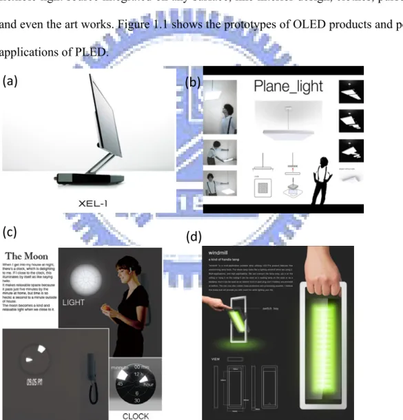
that of OLED now because of the earlier start of research in OLED, the fact that OLED grows up to maturity will bring up the PLED industry. Due to the low cost solution process compared with the thermal evaporation in OLED fabrication, PLED has potentials to be more competitive than OLED in many future applications.[5,6] PLED is also potentially to be flexible, which can be fabricated by roll-to-roll process with very high throughput and low cost for mass production.[7] The flexible PLED can be integrated on any surface. In addition to display technology, PLED can be used as a flexible light source integrated on any surface, like interior design, clothes, purses, cars, and even the art works. Figure 1.1 shows the prototypes of OLED products and potential applications of PLED.
FIG. 1.1: Potential applications of PLED. (a) OLED TV by Sony in 2007. (b) plane
light (c) light-weight and plane clock design (d) light-weight handle lamp. The concept of (b), (c) and (d) are provided by Inocell Creativity Center of Liteon Technology Corporation.
(b)
(a)
(d)
(c)
1.2 Optical and electric properties of π-conjugated materials
Conjugated polymers have their semiconducting properties with delocalized π-electron bonding along the polymer chain. The feature of π-conjugated compounds is single and double or single and triple bonds alternate throughout the molecule or polymer backbone.General speaking, the π bonds are formed from overlapping atomic pz orbital. The
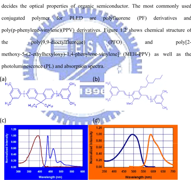
energy gap between the highest occupied molecular π orbital (HOMO) and the lowest unoccupied molecular π* orbital (LUMO) is typically in the range of 1.5-3 eV, which decides the optical properties of organic semiconductor. The most commonly used conjugated polymer for PLED are polyfluorene (PF) derivatives and poly(p-phenylene-vinylene)(PPV) derivatives. Figure 1.2 shows chemical structure of
the poly(9,9-dioctylfluorene) (PFO) and poly[2- methoxy-5-(2-ethylhexyloxy)-1,4-phenylene-vinylene] (MEH-PPV) as well as the
photoluminescence (PL) and absorption spectra.
FIG. 1.2: The chemical structure of (a) PFO and (b) MEH-PPV. The PL and absorption
spectra of (c) PFO and (d) MEH-PPV supplied by American Dye Source.
Compared with Si-based semiconductor, the organic thin films based on small molecules
(b)
(a)
(d)
(c)
or polymers are disorder. The transport properties in PLED are determined by inter-site hopping between localized states.[8] The field-dependent mobility is described as Poole-Frenkel form,
μ E, T μ T exp EE (1)
Where μ is the charge mobility, E is the electric field, μ0 is the low-field mobility and E0 are empirical coefficient.
1.3 PLED structure and operation
The basic structure of the PLED is so-called “sandwich structure” because the emissive layer (EML) is sandwiched between the anode and the cathode. The electron and hole inject from cathode and anode under bias, transport, and recombine in the EML.Figure 1.3 shows the common PLED device structure and schematic energy profile as well as the working principle.
FIG. 1.3: (a) Common PLED device structure. PEDOT:PSS is poly-(3,4- ethylene-
dioxythiophene):poly-(styrene sulfonate), which is the hole injection and hole transport layer. (b) Schematic energy diagram for basic PLED operation, including (i) carrier injection, (ii) carrier transportation, and (iii) recombination.
Glass substrate ITO PEDOT:PSS EML Cathode EML PEDOT:PSS Cathode Light emission (i) (i) (ii) (ii) (iii)
(a)
(b)
1.4 The efficiency of PLED
The most important issue now in PLED is the efficiency, not only for energy-consumption, but also for its effect on the lifetime of the device. The high efficiency allows a low IV product for a given luminance, resulted in longer device operating lifetime. The external quantum efficiency (EQE), which is defined as the number of photons emitted out of the device per injected electron.[9] In general, the EQE, ηEL, can be written as the following term:[10]
ηEL ξ γ rST ηPL (2)
Where ξ is the out-coupling efficiency, the ratio of the photons emitted out from the PLED; γ is the recombination ratio between electrons and holes, which is the same as exciton forming ratio; rST is the ratio of singlet excitons and triplet excitons formed from the recombining charge carriers; ηPL is the photo-luminescent quantum efficiency, which is the same as the radiative yield of singlet excitons.
There have been a constant progress in improving PLED efficiency from molecular and device structure designs.[5,11,12] Device models have been established and successfully explained many experiment results.[13,14] In general, there are two factors that determine the electroluminescence (EL) efficiency, including electron-hole charge balance in the diode and thin-film photoluminescence (PL) quantum efficiency of the luminescent materials. For PL quantum efficiency the most commonly used polymers based on PF derivatives and PPV derivatives, which all have very high PL quantum efficiency ranging from 15 % to 50 %. However, not all the materials with high PL efficiency will simultaneously yield high EL efficiency, indicating that the obstruction to high EL efficiency is charge balance. There are two elements which determine the individual charge currents. One is the carrier injection barrier and the other is the carrier
mobility. Much effort has been devoted to improving carrier injection, including electrode modification and adding hole (electron) injection layers.[15,16] For carrier mobility, the most unique and commonly known property of conjugated polymer is that the hole mobility is often much higher than the electron mobility.[17,18] Yet so far, there is no direct report focusing on the relation between carrier mobilities and EL efficiency. In this thesis, we have systematically studied and compared the charge balance of several PF and PPV based polymers which all have high PL quantum efficiency. In common high EL efficiency polymers have two distinguishing features: one is comparable electron and hole mobility, and the other is that electron current is even larger than hole current under uni-polar injection. This result confirms that many polymers have high PL efficiency but poor EL efficiency due to the low electron mobility and imbalanced currents between electron and hole. The huge difference in electron mobility among the polymers is attributed to extrinsic effects like impurity and molecular weight which causes electron traps but do not quench excitons and reduce PL.
1.5 The relation between molecular weight and device efficiency
In order to study the relation between electron mobility and molecular weight of materials, I have compared the device performance and estimated the electron mobility based on polymers with different molecular weights. PF derivative, PFO was chosen to be the emissive material since it has been extensively studied and very easy to synthesize. In addition, highly efficient blue PLED is critical to achieve white PLED through energy transfer by using the blue emitters as the host and red/green emitter as the dopants.[19,20] Deep blue PLED is more essential than the sky blue one in making white lights. However the deep blue material still remains a challenge due to their large band gap and difficulty in charge balance. Up to now, the highest reported efficiency fordeep blue PLED is about 3 cd/A by the Covion company with unavailable chemical structure.[21] The most well-known and commonly used materials for deep blue PLED are PF and its derivatives due to their high photoluminescence quantum efficiency.[22-24] However, they still suffer from low EL efficiency due to the poor charge balance caused by the difficulty in electron injection and transport. In addition, the color is unstable due to the formation of excimer in its liquid crystalline phase and ketone defect in the presence of oxygen.[25,26] It would greatly reduce the barriers to make high-performance blue PLED using simply PFO. The optical and morphological properties of PFO have been shown to depend sensitively on the molecular weight.[27] In general the higher molecular weight implies better stability and purity of the material. The low molecular weight polymers are also known to have poor color stability due to easier chain motions under device operation. Removal of the low molecular weight components is known to improve the performance.[28] So far the efficiency remains far lower than the Covion material even with molecular weight control. In this work we employ a high molecular weight PFO with Mw up to 365,000 to demonstrate a deep blue PLED with efficiency as high as 3.8 cd/A with corresponding external quantum efficiency 3.7 %, which is even better than the Covion blue PLED. Color stability is also improved relative to the low molecular weight counterpart. High molecular weight is found to enhance the electron current resulting in a better charge balance. Moreover, the efficiency is significantly enhanced by the doping of hole traps.[29] Instead of using a cross-linking polymer[30], a soluble hole-transport layer (HTL) is added by buffer liquid method[12] to increase the efficiency.
1.6 Broad band and white emission by adopting triplet emitter
In addition to fluorescent PLED, triplet emitter is needed to achieve high efficiency.Recently OLED has been demonstrated to reach nearly 100 % internal quantum efficiency by employing triplet emitters.[31,32] For this purpose, white light containing three primary colors is essential. Several ways to generate high-efficiency white light in PLED have been reported.[5,33] The spectra however usually contains only two peaks and has weak emission in the red, yielding low color rendering index (CRI). The CRI ranges from 0 to 100 and represents how authentic colors look when viewed with the light sources. For acceptable illumination sources, it needs to be higher than 80.[34-36] Ir complex is known to yield very high efficiency as doped into the polymer matrix.[37-39] It is therefore desirable to develop efficient white PLED with all three colors resulting from Ir complex emitter. So far high efficiency has been reported only for a single color, presumably due to the difficulty to distribute the recombination evenly among the three complexes as their carrier trapping capabilities could be very different. In this work we have studied PLED with multiple Ir complex doping in single and bilayer structures. Poly(vinylcarbazole) (PVK) blended with electron and hole transport molecules is used as the host.[40-43] It turns out that as the green phosphorescent dye tris- (2-4(4-toltyl) phenylpyridine (Ir(mppy)3) and red emitter bis (1-phenylisoquinoline) (acetylacetonate) iridium (III) (Ir(piq)2) were doped together the high efficiency was maintained with current efficiency 23 cd/A and emission spectral extending from 500
nm to 720 nm. As the blue dye (III) bis [(4, -6-di-fluorophenyl-pyridinato)N,C2]
picolinate (FIrpic) is added to the same layer there is no blue emission regardless of the concentration, probably due the much weaker carrier trapping by FIrpic compared with the green and red dyes. In order to obtain white emission a second blue layer is added with either phosphorescent dye Firpic doped in PVK or fluorescent polymer poly (9, 9-dioctylfluorene) (PFO) as the emitter. High color index of 86 and efficiency of 8.1 cd/A have been achieved.
1.7 Multilayer PLED fabrication
Recently OLED has been demonstrated to reach nearly 100 % internal quantum efficiency by employing triplet emitters and multilayer structures.[31,32] The multilayer device structure usually includes emissive, carrier transport, and carrier blocking layers. In general, a multilayer structure is required to balance the electron and hole currents. Although there have been impressive improvements in the carrier balance of PLED by molecular design[44,45], the efficiency is still below OLED. The main limit for PLED efficiency is the electron-hole imbalance. This problem can be solved in principle by multilayer hetero-junction structure. Compared with OLED by thermal evaporation there exists a problem that the solution process itself causes dissolution between spin-coated or ink-jetted polymer layers.[46-49] Therefore, the multilayer design is incompatible with the easy solution process so far. In the past few years, many strategies have been made to overcome the dissolution problems and make multilayer PLEDs.[6,50-53] Mostly the methods for multilayer deposition included three parts: 1. Weak solvent to reduce the dissolution problem of existing layer; 2. Cross-linking of polymer to make it insoluble; 3. Rinsing of the polymer by pure solvent after a hardening baking. A thin layer of insoluble polymer is left;the invention of multilayer fabrication process will be the most important part due to the fact that it realizes the multilayer device structure design by easy solution process. In this thesis two more ways were successfully applied for multilayer fabrication: Buffer liquid with high viscosity to cover the first layer as the second layer is deposited and blade coating with high speed. The buffer liquid method can completely prevent the dissolution between solution-processed polymer layers to fabricate high-efficiency and stable PLEDs by spin coating. However, there exists a material waste problem in spin coating process. The advantage of spin-coating is the good uniformity of thin film. Nevertheless the usage of materials is only 5% through
spin coating process. This raises dramatically the cost of PLED. In addition to the cost problem, the production of PLED through spin-coating is not efficient especially for large-area fabrication. In addition to spin-coating, there are several ways to form polymer thin films. The most common ways are slot coating and blade coating which are used to form polymer films with micrometer thickness like photo-resists and color-filters. There is no report about PLED fabrication by the slot coating and blade coating so far. In this thesis a blade coating method was successfully applied to make multilayer PLED. As a result, the performance of single layer device by blade coating is about the same as that by spin coating. Furthermore the performance of bilayer PLED by blade coating is better than that by spin coating.
Chapter 2
Multilayer device fabrication method,
sample preparing and sample measurement
2.1
Multilayer device fabrication process
The PLED can be made with solution process, which has potential for both large-area and low-cost fabrication. However the easy solution process is incompatible with multilayer PLED. In my study of multilayer PLED device design, the most important part is the way to achieve multilayer PLED design by easy solution process. Two ways have been successfully applied to make multilayer PLEDs, one is the liquid buffer layer (BL) method, and the other is the high-speed blade coating with an integrated heater. Both these two ways are physical way and easy to apply, no further chemical synthesis is needed.
2.1.1
Liquid buffer layer method
The material of the BL must be a viscous non-dissolvent liquid with relatively low boiling point. The viscosity is directly related to the protection capability. Before depositing the next polymer layer over an existing soluble polymer surface, the BL is first spin-coated. The next layer is then spun on top of the liquid surface of the BL. Because the viscosity of the BL is much higher than the usual solvent, the next layer will initially float over the BL instead of mixing with it. The polymer underneath is therefore protected by the BL against the solvent of the next layer. During the spinning most of the solvent of the next layer and part of the liquid BL are evaporated, resulting in a double-layer structure with possibly some residue of the BL in between. The residual BL is removed in the following
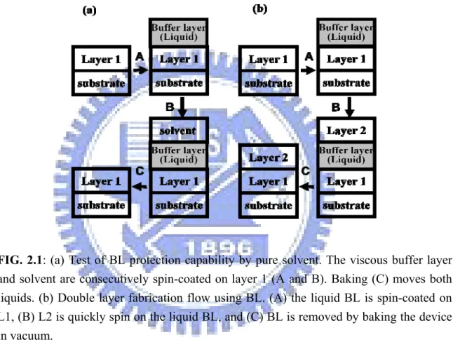
baking in vacuum. Therefore, besides the high viscosity, low boiling point and small molecule weight of BL are also important for easy removal by baking. If the boiling point is much higher than the polymer’s welting temperature, the required high baking temperature could damage the emissive polymer. The protection capability of many kinds of BL materials against various typical solvents such as xylene, toluene, and chloroform are studied as follows. Figure 2.1 (a) shows the steps.
FIG. 2.1: (a) Test of BL protection capability by pure solvent. The viscous buffer layer
and solvent are consecutively spin-coated on layer 1 (A and B). Baking (C) moves both liquids. (b) Double layer fabrication flow using BL. (A) the liquid BL is spin-coated on L1, (B) L2 is quickly spin on the liquid BL, and (C) BL is removed by baking the device in vacuum.
First, a polymer layer 1 (L1) is spin-coated on the substrate and baked in vacuum at 120 ℃ for 40 minutes. After spinning the BL on L1, we spin the pure solvent on the liquid surface immediately. The temporary layer structure is substrate/ L1/ BL/ solvent. After the evaporation of solvent and BL in air, we compare the L1 film thickness before and after the BL/solvent process. BL protection capability can be measured as the smallness of L1 thickness reduction. LUMATION* BP105 from The Dow Chemical Company
Light-Emitting Polymer (LEP) is chosen to be the test L1 material due to its high solubility in all common solvents. The dissolution for any other polymer under the same situation can only be less than BP105. The film thicknesses are measured by a Kosaka ET4000 Surface Profiler. Table 2.1 summarizes the results.
TABLE 2.1: The BL protection capability test. The test flow is shown in Figure 1 (a).
The viscosity and boiling point of each BL material are shown. Although the viscosity of 1,2-propylene glycol is low at room temperature, it increases rapidly when cooled down to 0 ℃. Glycerol has good protection capability as 1,2-propylene glycol, but its high boiling point is unfavorable for removal by baking.
Layer1 thickness (nm) a 200 200 180 106 103 (PFO) Buffer material b B1 B2 B3 No buffer B3 Boiling Point (℃) 290 188 128 - 128 Viscosity (η /mPa s) 934 (25℃) 248 (0 ℃) 0.508 (25 ℃) - 0.508 (25 ℃) Solvent c A B C A B C A B C A A Final thickness (nm) 200 200 200 200 200 200 60 60 70 20 22
a L1 is BP105 except the last column
b B1: Glycerol, B2: 1,2-Propylene Glycol, B3: n-Octane. c A: Xylene, B: Toluene, C: Chloroform.
Due to the high viscosity derived from hydrogen bonding, glycerol and 1,2-propylene glycol both have excellent protection capability. Even for the strong solvents like chloroform, they can perfectly protect L1 from the dissolution. On the contrary, n-octane has poor viscosity and the protection capability is not so good. Interestingly 1,2-propylene glycol combines the unique properties of high viscosity at 0 ℃ (248η/mPa s) and low boiling point (188 ℃), which are crucial for the protection and subsequent removal of BL as stated above. Because the viscosity of 1,2-propylene glycol decreases with temperature
dramatically, it is applied as buffer before cooling to 0 ℃.
The next step is to see whether the next polymer layer L2 can be spin-coated on L1 using the BL method. Below 1,2-propylene glycol is always used as the BL, BP105 is chosen to be both L1 and L2. The process flow is shown in Figure 1 (b). Ideally the final total thickness is the sum of the thicknesses of L1 and L2 as they are individually spin-coated on the substrate. Table 2.2 shows the thicknesses of the individual single-layers and double-layer polymer films.
TABLE 2.2: The thickness comparison between single layer and double layers. Layer 1
and Layer 2 are both BP105 dissolved in xylene. The thickness difference between the double-layer and the sum of Layer1 and Layer 2 is less than 7 nm.
Layer1 (nm) 120 120
Layer 2 (nm) 35 25
L1+L2 (nm) 155 145
Double-layer (nm) 148 140
Under the protection of the BL, the thickness difference between the double layer and the sum of L1 and L2 is less than 7 nm. The BL is therefore proved successful to fabricate a polymer multilayer structure without dissolution. Obviously this can be applied to arbitrary L1 and L2 in any solvent. Using this new method it becomes possible to make many kinds of multilayer PLEDs, which include not only PEDOT:PSS (HTL) and EML but also other functional layers like hole-blocking layer (HBL), electron-blocking layer (EBL), as well as electron transport layer (ETL) in order to optimize device efficiency.
2.1.2
Blade coating method
The working principle of multilayer fabrication process by blade coating is shown in Fig. 2.2(a). The thickness of the wet polymer layer is defined by the gap of blade coater. The polymer films are formed by blade coating and the dry film thickness can be tuned by the polymer concentration and the gap of blade coater. A heater is needed for multilayer process to expel the solvent of the second polymer solution as soon as possible. So the second film is formed by solution but quickly dried before dissolving the first polymer layer. The reason that the negative effect of the second layer to the first layer in blade coating is much smaller than the spin coating is that in the former the wet film thickness is only tens of microns while in the latter the initial liquid drop size is several milimeters which easily swallow the first thin film due to the large amount of solvent. A 70 nm poly(para-phenylene vinylene) (PPV) copolymer Super-Yellow (S-Y, supplied by Merck OLED Materials GmbH) thin film is first formed by blade coating in toluene solution with a scratch pattern ”NCTU” made by a cotton stick with solvent (toluene). Then poly(9,9-dioctylfluorene) (PFO, purchased from American Dye Source) solution is blade coated on top of the S-Y layer to form a 70 nm thin film. The sample is placed on a 70 ℃ hot plate as the second layer is blade coated for rapid solvent evaporation. The total thickness of S-Y/PFO bilayer is 150 nm measured by Kosaka ET4000 Surface Profiler, which is the same as the sum of the thickness of the individually blade coated S-Y and PFO layers. The NCTU pattern of the first S-Y layer is not damaged by the second PFO solution at all as shown in Fig. 2.2(b) under ultraviolet illumination, implying the mutual dissolution is minimal. The pattern will be completely destroyed if the PFO layer is deposited by spin coating. The lateral profile is checked by scanning electron microscope (SEM, JEOL JSM-6390LV). The result is shown in Fig. 2.2(c). It is clear that there exists an interface between the two polymer layers. The Al thin film is deposited on the PFO
layer to prevent the warp of polymer thin films during cutting.
FIG. 2.2: (a) Schematic working principle of multilayer structure by blade coating, the
process of second layer is on the hot plate. The solvent of the second layer is quickly evaporated without dissolving the first layer. (b) Double layer S-Y/PFO under ultraviolet illumination. The scratch pattern ”NCTU” is made by a cotton stick on the S-Y thin film before blade coating the PFO thin film. (c) The lateral profile of the double layer polymer film by SEM. There is no dissolution between these two polymer layers by blade coating.
In addition, Single layer PLEDs of the structure ITO/ PEDOT:PSS/ EML/ CsF/ Al were fabricated. S-Y and PFO were used for the EML and were dissolved in toluene. ITO substrates were cleaned and the surfaces were treated by oxygen plasma followed by spin-coating 50 nm of PEDOT: PSS. PEDOT:PSS film was baked at 200 ℃ for 5 minutes
in vacuum environment (10−3 torr). The PFO and S-Y thin film were annealed at 120 ℃
in vacuum (10−3 torr). All the devices were coated with CsF(2 nm)/Al(100 nm) cathode and packaged in a glove box.
2.2
Materials
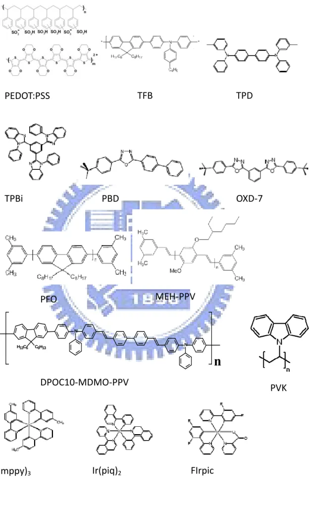
The basic PLED device contains four parts: the anode, electron/hole transport layers, the EML, and the cathode. The most common material for transparent anode, indium tin oxide (ITO) was used in this work. Before depositing the transport layers, PEDOT:PSS was always used for hole injection layer and hole transport layers, which can also flatten the ITO surface. For hole transport materials, poly[(9,9-dioctylfluorenyl -2,7-diyl)-co-(4,4’-(N-(4-sec-butyl phenyl)) diphenylamine)] (TFB; purchased from American Dye Source) and N,N’-diphenyl-N,N’-(bis(3-methylphenyl)- [1,1-biphenyl]- 4,4’diamine) (TPD) were used. 1,3,5-tris(N-phenylbenzimidazol-2-yl)benzene (TPBI), 2-(4-biphenylyl)-5-(4-tert-butylphenyl)- 1,3,4-oxadiazole (PBD), and 1, 3-bis [(4-tertbutylphenyl)- 1,3,-4-oxidiazolyl] phenylene (OXD-7) were used as electron transport materials. poly(9,9-dioctylfluorene)(PFO) with two different molecular weight (71,000 and 365,000), poly[(2-(4-(3,7-dimethyloctoxy)phenyl) -3-phenyl-1,4- phenylenevinylene)-co-(2,5-dimethoxy-1,4-phenylenevinylene)] (DPOC10 -DOMe- PPV; synthesized in our lab), poly[2- methoxy-5 (2’-ethylhexyloxy)- 1,4-phenylene vinylene] (MEH-PPV; purchased from American Dye Source), and other two materials with un-public chemical structures, which are SuperYellow (S-Y, supplied by Merck OLED Materials GmbH) and LUMATION BP105 from Dow Chemical Company, were used as the fluorescent emissive materials. Green emitter tris- (2-4(4-toltyl) phenylpyridine
(Ir(mppy)3), red emitter bis (1-phenylisoquinoline) (acetylacetonate) iridium (III)
(Ir(piq)2), and blue emitter (III) bis [(4, -6-di-fluorophenyl-pyridinato)N,C2] picolinate (FIrpic) were used as triplet emitters in the host polymer, Poly(vinylcarbazole) (PVK). As to the cathode, Ca/Al, LiF/Ca/Al. and CsF/Al were used by thermal deposition in vacuum. Figure 2.3 shows the chemical structures of the materials. Table 2.3 summarizes the materials used in this thesis.
FIG. 2.3: Chemical structures of the materials used in this thesis.
C6H13 H13C6 N N
n
PEDOT:PSS
TFB
TPD
TPBi
PBD
OXD‐7
PFO
MEH‐PPV
DPOC10‐MDMO‐PPV
PVK
TABLE 2.3: Summary of materials used in this thesis
Function Materials Work function
Or EA/IP (eV)
Function Materials Work function
Or EA/IP
Anode ITO 4.8 Singlet
Emitter
PFO 3.0/5.8
HIL PEDOT:PSS 5.0~5.2 DPOC10-DOMe-PPV 3.2/5.6
HTL/EBL TFB 2.3/5.3 MEH-PPV 2.8/4.9 TPD 2.3/5.5 S-Y 3.0/5.4 ETL/HBL TPBi 2.7/6.7 BP105 3.0/5.8 PBD 2.5/6.2 Triplet Emitter Ir(mppy)3 2.4/5.5 OXD-7 2.6/6.2 Ir(piq)2 2.5/5.3 Polymer host PVK 2.2/5.8 FIrpic 2.9/5.8
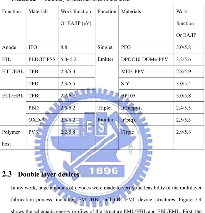
2.3
Double layer devices
In my work, huge amounts of devices were made to verify the feasibility of the multilayer fabrication process, including EML/HBL and EBL/EML device structures. Figure 2.4 shows the schematic energy profiles of the structure EML/HBL and EBL/EML. First, the double layer devices were made by liquid buffer layer method and then I studied the difference between liquid buffer layer method and blade coating method.
FIG. 2.4: Schematic electronic energy profile for the double-layer device structure of (a)
EML/HBL, and (b) EBL/EML.
Since many emissive conjugated polymers are p-type, and the hole mobility is two or three orders lager than electron mobility. Therefore the device structure ITO/PEDOT:PSS/EML/HBL/cathode to block the hole current and improve the device efficiency was adopted. Four typical p-type polymers were used as EML, including MEH-PPV, PFO, TFB and DPOC10-DOMe-PPV. For HBL, we chose two materials with good electron transport characteristic and large ionization potential (IP) to block holes. One was S-Y by Covion Organic Semiconductors[54], and the other was the small molecule TPBi. With the unusually large IP, TPBI is commonly used as the HBL in OLEDs by evaporation[55]. The structure of the device without HBL was glass/ITO/PEDOT/EML/LiF/Ca/Al, and the baking condition of EML was 180 ℃ for TFB and 120 ℃ for the other EML for 40 minutes in vacuum. The structure of the device with HBL was glass/ITO/PEDOT/EML/HBL/LiF/Ca/Al, and the baking condition of EML was the same as the devices without HBL. After the HBL was spin-coated on the EML using BL method, the devices were baked in vacuum for 60 minutes at 200 ℃ for DPOC10-DOMe-PPV and 120 ℃ for the other EML. Then the devices were coated with LiF/Ca/Al cathodes and packaged in the glove box.
(a)
(b)
EML PEDOT:PSS Cathode Light emission EBL HBL EML PEDOT:PSS Cathode Light emissionIn addition to the EML/HBL structure, EBL/EML structure was also made. In this experiment, TFB was chosen as the material of EBL and LUMATION BP105 was chosen as the blue polymer. BP105 is currently very good blue polymer for PLED. Even so the electron-hole balance is far from perfect. In single layer LED the current is dominated by electron current because of the high electron mobility and large hole injection barrier. Such imbalance was evidenced by the much smaller hole-only current than the LED current to be determined by the comparison of hole-only and electron-only devices. Four kinds of devices were made to present the advantage of the buffer method. The first two were ITO/PEDOT: PSS/TFB/EML/Cathode made by the BL method and the spin-rinse method.[52] The second two were ITO/PEDOT: PSS/EML/Cathode made by pure BP105 or BP105: TFB blend (10:1). The ITO substrates were cleaned and the surfaces were treated by oxygen plasma followed by spin-coating 50 nm of PEDOT:PSS. PEDOT:PSS film was baked at 200 ℃ for 5 minutes in vacuum environment (10−3 torr). TFB film (30 nm) was spin-coated on PEDOT: PSS film (1% in xylene) and annealed at 180 ℃ in vacuum for 40 minutes. For the BL method, a 67 nm BP105 film was spin-coated (2% in xylene) over the liquid buffer covering TFB. The double-layer device was baked at 120 ℃ for 1 hour in vacuum to remove the residue 1,2-propylene glycol. Since the size of 1,2-propylene glycol molecules is about the same as common organic solvents like xylene, there should be no problem for them to diffuse across the layer 2 polymer during annealing. In fact any significant residue of 1,2-propylene glycol at the interface would be detrimental to the device performance. The excellent performance to be discussed below is another evidence for the complete removal of the buffer liquid. There was no loss in the double-layer film thickness compared with the sum of the two individual films within the error of thickness measurement. In other words, the inter-diffusion of the two polymers was less than the experimental error of the individual thickness, which was about 5 nm. For the spin-rinsing method, a very thin TFB layer (about 10 nm) was achieved by
spin-rinsing the TFB layer with pure xylene to remove the remaining soluble part. A 67 nm BP105 film was then spin-coated on the spin-rinsed TFB layer and baked at 120 ℃ for 40 minutes in vacuum. For the other devices the EML films were baked in vacuum for 40 min at 120 ℃. Finally all the devices were coated with LiF/Ca/Al cathode and packaged in the glove box.
In order to verify the feasibility of multilayer PLED by blade coating, bilayer PFO devices were made with the structures ITO/PEDOT:PSS/TFB/PFO/CsF/Al and ITO/PEDOT/PFO/PBD/CsF/Al. Both TFB and PBD were dissolved in toluene. TFB film (30 nm) was spin-coated on PEDOT:PSS film and annealed at 180 ℃ in vacuum for 40 minutes. PFO was blade coated on top of TFB layer on hot plate at 70 ℃. PBD was blade coated on PFO layer on hot plate 100 ℃. The thickness of PFO was about 80 nm. All the devices are coated with CsF(2 nm)/Al(100 nm) cathode and packaged in a glove box.
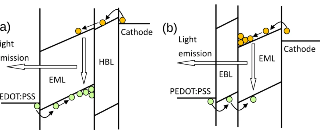
2.4
Hole-only devices, electron-only devices, and the way to obtain carrier mobilityHole-only and electron-only devices are very useful tools to study and to compare the hole currents and electron currents among different materials. Although these can not represent the real hole currents and electron currents in the bipolar devices, they provide a tool to study the hole mobility and electron mobility of the materials individually. Figure 2.5 shows the schematic energy profile of hole-only and electron-only devices.
FIG. 2.5 : Schematic electronic energy profile for uni-polar devices, (a) Hole-only (b)
Electron-only devices.
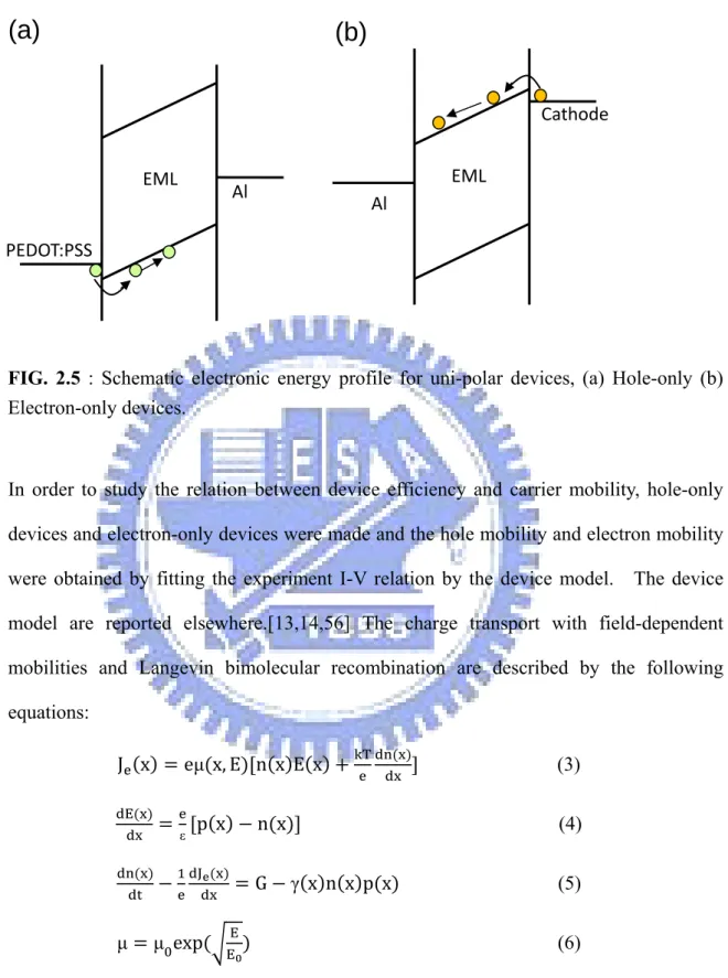
In order to study the relation between device efficiency and carrier mobility, hole-only devices and electron-only devices were made and the hole mobility and electron mobility were obtained by fitting the experiment I-V relation by the device model. The device model are reported elsewhere.[13,14,56] The charge transport with field-dependent mobilities and Langevin bimolecular recombination are described by the following equations: J x eμ x, E n x E x T (3) E ε p x n x (4) J G γ x n x p x (5) μ μ exp EE (6)
where Je is electron current density, n is the density of electron and p is the density of hole, E is electric field, ε is permittivity of materials, k is Boltzmann’s constant, G is the electron-hole pair generation rate, and γ is the recombination coefficient. We assume G is
EML PEDOT:PSS Al EML Al Cathode
(a)
(b)
negligible due to the large band gap of polymers. Eq. (3) describes the net current of electron (holes analogous), combined with drift and diffusion terms. Eq. (4) is Poisson equation. The electron continuity equation, Eq. (5), contains the bimolecular recombination term γ x n x p x , where γ is in the Langevin form γ eμm⁄ and με m is the larger one of μe or μp. The field-dependent mobility is described as Poole-Frenkel form, Eq. (6), where μ0 and E0 are fitting parameters. In this work, we also consider the tunneling current with Fowler-Nordheim (FN) injection:
Jtu BE2 8π√2m φ
3 2⁄
3heE (7)
where m* is the electron effective mass, φ is the energy barrier, h is Planks constant and B is the coefficient that contains the tunneling prefactor and the rate for current backflow. The value of B in Eq. (5) is taken from the fitting data for carrier tunneling from
electrodes.[57]Once the energy levels of the polymers and electrodes are known, the
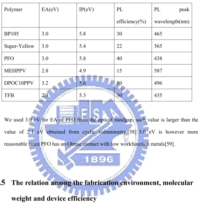
carrier mobility can be obtained by fitting the experimental I-V relations of uni-polar devices and the model calculation. In this work, three kinds of devices were studied, including hole-only device, electron-only device and bipolar device. Hole-only and bipolar device structures were ITO/PEDOT:PSS/polymer/Al and ITO/PEDOT:PSS/polymer/LiF/Ca/Al, respectively. Electron-only device structure was Al/polymer/LiF/Ca/Al. Polymers were dissolved in organic solvent like xylene or toluene and then spin coated to make a 100nm thin film followed by a baking process in vacuum (10−3 torr) at 120 ℃. The anode and cathode metals were evaporated by a evaporator in a glove box in high vacuum (< 10−6 torr). Finally, all the devices were packaged in the glove box. In this work six polymers were chosen to study the properties of transport and EL efficiency. Two high efficiency polymers, LUMATION BP105 and S-Y, and the other four less efficient polymers, including PFO, TFB, DPOC10PPV, and MEH-PPV were studied. The electron affinity (EA), ionization potential (IP), PL efficiency and PL
wavelength of polymers are shown in Table 2.4.
TABLE 2.4: EA, IP, PL efficiency and PL wavelength of polymers in this part.
Polymer EA(eV) IP(eV) PL efficiency(%) PL peak wavelength(nm) BP105 3.0 5.8 30 465 Super-Yellow 3.0 5.4 22 565 PFO 3.0 5.8 40 438 MEHPPV 2.8 4.9 15 587 DPOC10PPV 3.2 5.6 50 496 TFB 2.3 5.3 30 435
We used 3.0 eV for EA of PFO from the optical bandgap, such value is larger than the
value of 2.1 eV obtained from cyclic voltammetry.[58] 3.0 eV is however more
reasonable since PFO has an Ohmic contact with low workfunction metals[59].
2.5
The relation among the fabrication environment, molecular
weight and device efficiency
PFO is a well-known light-emitting polymer, and many researches have been down on this material. Therefore I made single layer devices and double layer devices based on PFO to study the relation among the fabrication environment, molecular weight and device efficiency. In this part, two PFO with different molecular weight (71,000 and 360,000) were chosen, and I named the high molecular weight PFO as HMw-PFO for clarity.
2.5.1
The relation between the fabrication environment and
device efficiency
In the first step, I studied the relation between the fabrication environment and efficiency. Six bipolar devices and two electron-only devices were fabricated. The hole transport and emissive polymers were spin-coated in air for some devices and in the glove box for other devices. For bipolar devices made in air, A was ITO/ PEDOT:PSS/ PFO/ LiF/ Ca/ Al, B was ITO/ PEDOT:PSS/ TFB/ PFO/ LiF/ Ca/ Al, C was ITO/ PEDOT:PSS/ PFO/ CsF/ Al, D was ITO/ PEDOT:PSS/ TFB/ PFO/ CsF/ Al. For bipolar devices made in the glove box, E was ITO/ PEDOT:PSS/ PFO/ CsF/ Al and F was ITO/ PEDOT:PSS/ TFB/ PFO/ CsF/ Al. For electron-only devices, G was Ag/ PEDOT:PSS/ PFO/ Ca/ Al made in air and H was Ag/ PEDOT:PSS/ PFO/ Ca/ Al made in glove box. TFB (Mw=197000) and PFO (Mw=71000) were both purchased from American Dye Source and used without further purification. PEDOT:PSS layer was spin-coated on a patterned ITO substrate and baked at 200 ℃ in vacuum (10−3 torr) for 5 minutes. TFB dissolved in toluene was spin-coated to make a 30 nm thin film and then baked at 180 ℃ in vacuum (10−3 torr) for 40 minutes to remove the solvent. PFO was also dissolved in toluene and then spin-coated to make a 70 nm thin film for bilayer devices (device B, D and F) and 90 nm for single layer devices (device A, C, E, G and H). To prevent dissolution in the bilayer structure, a liquid buffer, 1,2-propylene glycol, was used between TFB and PFO layer. For bilayer structure PFO layer was baked in vacuum (10−3 torr) at 120 ℃ for 1 hour to remove the residual glycol and organic solvent. For single layer structure PFO layer was baked for 40 minutes. Two kinds of cathodes were chosen and compared: LiF/Ca/Al and CsF/Al. The thickness was 2 nm for both LiF and CsF, 35 nm for Ca and 100 nm for Al. All the devices were packaged in the glove box.
2.5.2
The relation between the molecular weight and device
efficiency
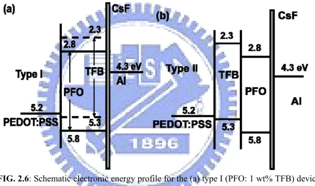
In the second step, I studied the relation between molecular weight and device efficiency. In this part, three types of device were fabricated, including the doped host-guest emission layer (EML) in single layer structure (type I), HTL/EML bilayer device (type II), and HTL/host-guest EML bilayer device (type III). Fig. 2.6(a) shows the schematic energy profile for type I devices and Fig. 2.6(b) for type II.
FIG. 2.6: Schematic electronic energy profile for the (a) type I (PFO: 1 wt% TFB) device
structure (b) type II (TFB/ PFO) device structure. The numbers are in eV.
PFO (Mw=71,000) and high molecular weight HMw-PFO (Mw=365,000) purchased from American Dye Source (ADS) were chosen as light-emitting polymers without any further purification. TFB were chosen as dopant for type I devices and HTL for the bilayer devices (type II and type III). Single layer PLEDs based on PFO and HMw-PFO without any TFB were made as standard devices. All PLED devices were fabricated on glass substrates with PEDOT:PSS layer on a patterned ITO layer. For type I devices 1 wt% of TFB was blended into PFO and HMw-PFO individually as the dopant. The film
was formed by spin-coating and baking at 120 ℃ in vacuum (10−3 torr) for 40 minutes to remove the solvent. For type II and type III devices TFB dissolved in toluene was
spin-coated to make a 30 nm thin film then baked at 180 in vacuum for 40 minutes. ℃
PFO and HMw-PFO were also dissolved in toluene and spin-coated to make bilayer devices (type II an III) by a liquid buffer layer to prevent the dissolution problem. For the
bilayer structure, PFO layer was baked in vacuum at 120 for 1 hour to remove the ℃
residual 1,2-propylene glycol liquid buffer and organic solvent. Except for the PEDOT:PSS layer all the fabrication processes were carried out in the glove box to reduce oxygen adsorption of PFO. CsF (2nm) /Al (100nm) were deposited as cathode by thermal evaporation. Finally all devices are packaged in the glove box.
2.6
Multilayer phosphorescent PLED
Phosphorescent light-emission can be achieved by adding triplet emitters in to the polymer host. The triplet emitters are usually the heavy metal complexes, which can change the spin-orbital states and let the non-emission triplet exciton decay with illumination. It is believed that phosphorescent PLED is a promising way for high efficiency. In general, most the phosphorescent PLEDs use only one triplet emitter in one device. Rare studies report one PLED has two or more triplet emitters. In this part I
studied four kinds of PLED, including a green one based on Ir(mppy)3 (device I), a
yellow broad-band one based on Ir(mppy)3 : Ir(piq)2 (device II) and two white ones based on Ir(mppy)3 : Ir(piq)2/ blue (phosphorescent or fluorescent) bilayer structure (device IV).
Ir(mppy)3 was purchased from American Dye Sources , Ir(piq)2 and FIrpic were
purchased from Luminescence Technology Corporation. Ir(mppy)3 and Ir(piq)2 were
doped into PVK host blended with TPD, and PBD. TPD and PBD were functional materials to enhance carrier transporting ability. FIrpic acted as the blue phosphorescent
emitter and was doped into PVK host with OXD-7 to enhance the electron transporting ability.[60] PFO (Mw= 365,000) was chosen as the blue florescent emitter. TFB (Mw=197,000) was used as hole injection layer. The PLED devices were fabricated on glass substrates with patterned ITO layer. The ITO glass was cleaned in acetone and then exposed to UV-ozone for 20 minutes. Then 50 nm hole injection layer of Poly-(3,4- ethylenedioxy thiophene) doped with Poly (styrene sulfonate) (PEDOT: PSS, Baytron P
CH 8000) was spin coated and annealed at 100 for 40 minutes. TFB dissolved in ℃
toluene was spin coated on PEDOT: PSS layer and annealed at 180 for ℃ 40 minutes to
remove the residual solvent, then spin-rinsed by toluene to remove the dissolvable part. Afterwards, the blended emission layer for green light was deposited by spin coating to
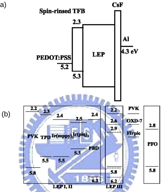
form a 70 nm thin film for device I then baked for 60 minutes at 80 . For device to ℃
ensure better solubility of FIrpic and PVK and spin coated directly upon the blended emissive layer to form a 45 nm thin film and followed by annealing at 80 for 1hour. ℃ The high molecular weight PVK (Mw=1,100,000) has poor solubility for toluene solution, so the mutual dissolution could be negligible. For white light device IV, PFO was dissolved in toluene and spin coated upon the blending emissive layer to form a 40 nm thin film and then annealed at 120 for 1 hour. All the procedures ℃ were performed in air. The CsF (1 nm) /Al (100 nm) cathode for device I, II, IV and CsF (2 nm) /Al (100 nm) for device III were evaporated onto the emissive layer under vacuum at the pressure of 8×10⁻⁷ torr. Fig. 2.7(a) shows the energy profile of the materials use in this work.[61-63] LEP represented light-emitting polymer which is in general a blend of various materials.
The LEP weight blending ratio was PVK:PBD:TPD: Ir(mppy)3=61:24:9:6 for device I,
PVK:PBD:TPD: Ir(mppy)3: Ir(piq)2=61:24:9:6:0.34 for device II, PVK:PBD:TPD:
Ir(mppy)3: Ir(piq)2=61:24:9:3:12 for device III and PVK:PBD:TPD: Ir(mppy)3:
Ir(piq)2=61:24:9:3:3 for device IV. The EA and IP of polymer used in this article are shown in Fig. 2.7(b).
FIG. 2.7: (a) Schematic energy level diagram of the device. (b) Electron affinity and
ionization potential of materials used in this work. Numbers are given in eV
2.7
The device encapsulation process
In the packaging a UV adhesive (XNR5516ZHV-B1, purchased from Nagase- Chemte X) was used to fix a piece of cover glass on the substrate. Then the device was exposed to UV light to harden the adhesive and block the oxygen and moisture in air. The whole process was completed in nitrogen atmosphere.
(a)
2.8
Measurements
The film thickness was measured by measured by Kosaka ET4000 Surface Profiler. The microscopic uniformity was checked by scanning electron microscope (SEM, JEOL JSM-6390LV) and atomic force microscope (AFM). The EL characteristics of the device were measured with Keithley 2400 and PR650 Spectroscan spectrometer. The CIE coordinates and CRI of the white PLED were calculated with the PR650 software. All the measurements were carried out in ambient air after packaging.
Chapter 3
Results and Discussion
3.1. Double layer devices with HBL by liquid buffer method
In the first step, several kinds of HBL were added on the common p-type light-emitting polymers by liquid buffer method to verify its feasibility. The device structure is ITO/ PEDOT:PSS/ EML/ HBL/ cathode. Four typical p-type polymers were used as EML, including MEH-PPV, PFO, TFB and DPOC10-DOMe-PPV. For HBL, we chose two materials with good electron transport characteristic and large ionization potential (IP) to block holes. One was S-Y, and the other was the small molecule TPBi. The fabrication process is described in page 20. Figure 3.1 shows the results for MEH-PPV PLED with and without the Super Yellow as HBL. MEH-PPV was dissolved in xylene and S-Y was dissolved in toluene. The MEHPPV thickness was 70 nm and S-Y thickness was 30 nm.
FIG. 3.1: The performances of MEH-PPV LED (solid circle) and MEH-PPV/Super
Yellow (S-Y) LED (open circle) made by liquid buffer method.
From the EL spectrum, the device with HBL is almost the same as that without HBL, indicating that most holes cannot go through the barrier at the MEH-PPV/S-Y interface and recombine in the highly luminescent Super Yellow. Even though the holes were blocked by S-Y, the current did not become smaller, which is probably due to the emergence of large recombination current occurring in the hole accumulation region near
the barrier. The maximum luminance was increased form 491 to 1611 cd/m2, and the
current efficiency was enhanced from 0.33 to 0.66 cd/A. The relatively low efficiency of single layer LED is probably because no purification was made and the molecular weight was low. The second example was green DPOC10-DOMe-PPV as EML and TPBI as HBL, both dissolved in toluene. The DPOC10-DOMe-PPV thickness was 120 nm without TPBI and 80 nm with TPBI (30 nm). The maximum luminance was increased
from 6367 to 14820 cd/ m2, which is shown in Figure 3.2. The device efficiency was
FIG. 3.2: The performances of DPOC10-DOMe-PPV LED (solid circle) and
DPOC10-DOMe-PPV/TPBI LED (open circle). The chemical structure of DPOC10-DOMe-PPV is shown.
For blue polymers, the I-L-V curves of PFO PLED with and without TPBI HBL are shown in Figure 3.3. Both PFO and TPBI were dissolved in toluene. The PFO thickness was 130 nm without TPBI and 60 nm with TPBI (45 nm).
FIG. 3.3: The performances of PFO LED (solid square), PFO/TPBI LED (open square),
TFB LED (solid circle) and TFB/TPBI LED (open circle). The EL spectra are normalized to 2 for TFB device (solid triangle) and 1 for PFO device (open triangle) for clarity.
The maximum luminance was again significantly improved from 278 to 1483 cd/ m2, and
the current did not become smaller. The current efficiency was enhanced form 0.61 to 1.45 cd/A. An even more dramatic case is TFB, also shown in Figure 3.3. TFB was dissolved in xylene and TPBI was dissolved in chloroform. The TFB thickness was 86nm
and TPBI thickness was 35nm. The maximum luminance was enhanced from 298 to 2271 cd/ m2, and the current efficiency from 0.05 to 0.47 cd/A. The general feature of all the devices is that the HBL significantly improves the efficiency and luminance while the current remains about the same. The turn-on voltage is also remarkably reduced for all devices with HBL. The lifetime and uniformity of the bilayer devices are not degraded relative to the single layer ones, indicating complete removal of the buffer liquid by annealing. The above results not only open the possibility of all solution-processed multilayer PLEDs through buffer layer method, but also show the LED thus made indeed significantly exceed the conventional single-layer device for four typical orange, green and blue emissive polymers. This method is very easy to apply and does not involve any process other than spin-coating and baking. There is no need to design and synthesize new functional materials. One can simply choose the combinations of existing materials with desired properties as long as they can be dissolved in some solvent.
3.2. Double layer devices with EBL by liquid buffer method
Common light-emitting polymers are p-type, which means the device current is dominated by hole currents. In these p-type polymers, HBL is needed to improve the efficiency. On the contrary, for the n-type materials, EBL is needed to block the huge amount of electrons to improve the efficiency. In this work, BP105 was chosen to be the n-type light-emitting polymer and TFB was chosen to be the EBL. Four kinds of devices were made to present the advantage of the buffer method. The first two were ITO/PEDOT: PSS/TFB/EML/Cathode made by the BL method and the spin-rinse method.[52] The second two were ITO/PEDOT: PSS/EML/Cathode made by pure BP105 or BP105: TFB blend (10:1). The fabrication process is described in page 21. Figure 3.4 shows the results of the four kinds of blue PLEDs.
FIG. 3.4: The performances of blue PLED: single layer BP105 (solid circle),
double-layer TFB/BP105 with BL process (open circle), spin-rinsed TFB/BP105 (solid triangle), BP105 blending with TFB (open triangle). (a) The current efficiency. Inset are the EL spectrum and TFB chemical structure. (b) The luminance. Inset is the current density.
Note the current for hole-only BP105 device (PEDOT/BP105/Al, solid star) is much smaller than the single layer LED current, indicating dominance of electron current