Methods of determining the contact between a probe and a surface under scanning
electron microscopy
C.-H. Nien, C. H. Tsai, K. Y. Shin, and W. B. Jian
Citation: Review of Scientific Instruments 77, 103709 (2006); doi: 10.1063/1.2360883
View online: http://dx.doi.org/10.1063/1.2360883
View Table of Contents: http://scitation.aip.org/content/aip/journal/rsi/77/10?ver=pdfcov Published by the AIP Publishing
Articles you may be interested in
Silicon photodiodes for low-voltage electron detection in scanning electron microscopy and electron beam lithography
J. Vac. Sci. Technol. B 24, 2951 (2006); 10.1116/1.2363405
Shape dependent thermal effects in apertured fiber probes for scanning near-field optical microscopy J. Appl. Phys. 99, 084303 (2006); 10.1063/1.2188250
High-speed and high-precision deflectors applied in electron beam lithography system based on scanning electron microscopy
J. Vac. Sci. Technol. B 22, 3557 (2004); 10.1116/1.1813454
Scanning tunneling microscopy studies of the Fe 3 O 4 (001) surface using antiferromagnetic probes J. Appl. Phys. 93, 7142 (2003); 10.1063/1.1556199
Observation of selective thermal desorption of electron stimulated SiO 2 with a combined scanning reflection electron microscope/scanning tunneling microscope
J. Appl. Phys. 82, 639 (1997); 10.1063/1.365592
Methods of determining the contact between a probe and a surface
under scanning electron microscopy
C.-H. Niena兲
Department of Physics, National Central University, Zhongli, Touyuan 320, Taiwan
C. H. Tsai and K. Y. Shin
Department of Engineering and System Science, National Tsing Hua University, Hsinchu 300, Taiwan
W. B. Jian
Department of Electrophysics, National Chiao Tung University, Hsinchu 300, Taiwan
共Received 28 June 2006; accepted 10 September 2006; published online 24 October 2006兲 Based on the charging effect common to various kinds of electron microscopy, we have developed novel methods of determining “when” and “where” a probe starts to contact an electrically isolated surface. The touchdown of an electrically grounded probe leads to an acute change in the imaging contrast of the contacted surface, which also causes a rapid jump 共ranging from a few to tens of picoamperes兲 of the grounding current. Thus, the detection of contact can be carried out in both qualitative and quantitative manners, providing a basis for establishing relevant standard procedures. In addition, we have achieved the spatial mapping of the contact point共s兲 using a specially designed lithographical pattern with two mutually vertical sets of parallel conductive lines. The precision of this mapping technique is simply determined by the pitch of parallel lines, which can be as small as the capability achievable in e-beam lithography. A possible “one-probe” version of the electrical characterization is also discussed with the same underlying principle, which may turn out to be indispensable for various studies and applications of nanostructures. Further development along this track is promising to realize an instrumentally simple version of “scanning electron spectroscopy” with various modes. © 2006 American Institute of Physics.
关DOI:10.1063/1.2360883兴
I. INTRODUCTION
The evolution of scanning electron microscopy 共SEM兲 has gone through a long way to bring us a versatile tool for microscopic investigation. In addition to the basic function of imaging microscopic structures down to nanometer scale, SEM has been further developed by many efforts to possess various optional modes of microanalysis, most of which de-mand some sophisticated devices.1 In contrast, it was not until a few years ago when multiprobe systems operated in-side SEM started to gain an increasing attention from the community of both nanoscience and nanotechnology.2 On the one hand, SEM-based multiprobe systems are probably the most literal tools of nanomanipulation for scientists. The relative ease of sample preparation and the manipulation with a real-time watching also contribute major advantages of this development over other competitive approaches based on the transmission electron microscope3 共TEM兲 and the atomic force microscope 共AFM兲,4 respectively. Among the reported scientific achievements based on the SEM-based multiprobe systems are the attempts to manufacture nanos-cale structures 关e.g., the attachment of carbon nanotubes 共CNTs兲 onto a tip for scanning probe microscopes5 共SPMs兲 or field-emission properties兴6
and the efforts to study the me-chanical or electrical properties of nanostructures 共e.g., the
conductivity of nanowires by the standard four-probe measurement兲.7
On the other hand, more and more routine tasks共e.g., the quality control of products兲 for engineers in the semiconductor industry have also become dependent upon the SEM-based multiprobe systems to serve as the elec-trical probing tool for their submicron electronics.8
At this stage, however, some basic techniques relevant to the performance of this advanced instrument are still far from maturity. For instance, the establishment of contact be-tween the probes and the target features on the substrate surface, a vital step when this instrument acts as an electrical probing system, still relies greatly on a primitive trial and error. To the best of our knowledge, the current way of run-ning a SEM-based multiprobe system is to keep a sharp tip of the probe in some tilted orientation all the time, so that one can track the very end of the probe共which is presumed to be the contact point兲 by watching the real-time SEM image.6As for the moment of contact, it may not be sensed until some visible lateral slips or damages occur.
In this article, we present some simple but effective so-lutions to these problems for a multiprobe system operated inside SEM. Based on the charging effect common to various kinds of electron microscopy,1we demonstrate our methods of determining “when” and “where” a probe starts to contact an electrically isolated surface. A possible “one-probe”
ver-a兲Author to whom correspondence should be addressed; electronic mail: [email protected]
0034-6748/2006/77共10兲/103709/7/$23.00 77, 103709-1 © 2006 American Institute of Physics
sion of the electrical characterization with the same underly-ing principle is also explored for its potential applications to the studies of nanostructures.
II. PRINCIPLE OF OPERATION
Instead of trying to avoid the “charging effect” at the first place by getting the samples grounded in one way or another, we first keep the samples electrically isolated from the ground 共i.e., electrically disconnected from the sample holder兲 while the probe is connected to the ground through an ammeter, as depicted in Fig. 1. Upon imaging by the scanned electron beam, the samples will suffer the expected charging effect due to their electrical isolation from the ground, resulting in a poor contrast of the samples in the image, as depicted in Fig.1共a兲. This situation will change as soon as the electrically grounded probe is brought to touch a sample, leading to the effective depletion of previously ac-cumulated charges. Depending on the electrical property of this sample共among other factors兲, the event of contact will then cause a corresponding change of contrast to various extents, as depicted in Fig.1共b兲. Furthermore, we also expect a corresponding change 共upon contact兲 for the “grounding current,” which is the flow of electrons between the sample surface and the ground as a result of the continuous impinge-ment of the electron beam. Note that the grounding current bypasses the conventional way共via the sample holder兲 and goes through an ammeter in the configuration of our meth-ods, which turns out to share the same underlying concept with a long recognized mode共usually termed the “specimen current” or “adsorbed current”兲 available for SEM-based microanalysis.1 Nevertheless, the temporary connection of the sample to the ground through a maneuverable probe, a technical feature unique to our approach, is likely to provide greater opportunities of various novel techniques for nanos-cale applications.
In addition to determining when a probe starts to contact an electrically isolated surface, we have also developed a method to answer the question about where the contact site共s兲 is 共are兲 located. Unlike the relative mapping 共to the imaged field itself only兲 as provided by a scanning probe microscope 共SPM兲, our method allows the absolute loca-tion共s兲 of the contact point共s兲 to be mapped with respect to either the sample surface or the probe itself. Again, our method of mapping the contact point共s兲 takes advantage of the charging effect with a specially designed lithographical
pattern共to serve as the tool of calibration兲. Ideally, the most straightforward structure for this pattern to function is prob-ably as complex as the conceptual design depicted in Fig. 2共a兲, where two sets of parallel conductive lines are litho-graphically fabricated共on top of the same surface of interest or a surface with the same orientation兲 so that the lines be-longing to one set cross on top of those bebe-longing to the other. Moreover, these conductive lines are electrically iso-lated from the ground as well as from each other 共say, by sufficiently thick layers of insulating oxide兲. In the case of a single contact site, the touchdown of the probe onto this pattern will change the imaging contrast of two crossed lines, indicating the location of the contact point关as illustrated in Fig.2共b兲兴. Note that the identified contact point with respect to the probe itself will remain the same as long as the probe keeps its orientation while exploring a sufficiently flat area having a common surface normal with the calibrating pat-tern. In principle, we can therefore achieve a precise contact with the spatial uncertainty determined solely by the pitch of this calibrating pattern 共regardless of how blunt the probe might be兲. As a result, the requirement of a sharp tip can now be eliminated for whatever applications involving contact of the probe with a sufficiently flat surface.
Having considered the relatively high demand of labor and technical skill for fabricating the conceptual version of our calibrating pattern, we are further committed to propose a more practical version with a much simpler structure, re-sulting in a lower failure rate of fabrication and a better durability. The pattern of this alternative version is also com-posed of two sets of parallel conductive lines, the common direction of which in one set is vertical to that in the other. However, these two sets of lines are now patterned side by side关as depicted in Fig.2共c兲兴 instead of crossing each other with an insulting layer in between. Consequently, the map-ping procedure will now involve the touchdown of the probe onto one set of parallel lines to determine the first coordinate of the contact point共s兲, followed by the touchdown onto the other set of parallel lines to determine the second coordinate. This two-step procedure 共instead of only one step for the conceptual version兲 of mapping can be regarded as a little price to pay in operation for saving a lot of efforts in fabri-cating the corresponding pattern.
FIG. 1. The basic configuration and the working prin-ciple of our methods. Three conductive samples are electrically isolated from the ground, and the conduc-tive probe is connected to the ground through an am-meter.共a兲 The “charging effect” of all samples 共due to their electrical isolation from the ground兲 upon imaging by the scanned electron beam. It causes a poor imaging contrast of all samples.共b兲 A sensible change in the imaging contrast of the contacted sample surface and the corresponding change of the “grounding current” upon touchdown of the probe.
103709-2 Nien et al. Rev. Sci. Instrum. 77, 103709共2006兲
III. EXPERIMENTAL RESULTS
The SEM-based multiprobe nanoelectronics measure-ment system in this work is composed of JOEL-7000 field-emission SEM equipped with a four-nanoprobe system 共manufactured by Kammrath & Weiss, Germany兲. The mea-surement of the grounding current is done by a Keithley 4200-SCS to serve as the ammeter with a resolution better than 0.1 pA.
We have followed the standard procedure of e-beam li-thography to fabricate a calibrating pattern with our practical version. In this testing pattern, the conductive lines with a pitch of 500 nm were made of gold strips of 100 nm thick and 200 nm wide deposited onto an insulating oxide layer 共of 1000 nm thick兲 on top of silicon wafer. A square pattern 共with a size of 400⫻400m2兲 of gold film was also fabri-cated in the same way to test our methods of detecting the events of contact.
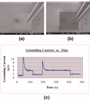
An example of determining the contact of probes with our method is illustrated in Fig.3, where the surface feature is a square pattern of gold film共of 100 nm thick, with a size of 400⫻400m2兲 deposited onto an insulating oxide layer 共of 1000 nm thick兲 on top of a silicon wafer. As clearly shown in Figs.3共a兲and3共b兲by SEM images, the touchdown of an electrically grounded probe leads to an acute change in the imaging contrast of the contacted surface共i.e., the con-ductive gold square兲. We have also confirmed the existence of the corresponding change共approximately a few picoam-peres兲 in the grounding current, as illustrated in Fig.3共c兲for two times of touchdown. In this way, the same event of con-tact that induces a sudden change of the imaging contrast in Fig.3共b兲is also found to cause a rapid jump共approximately a few picoamperes兲 of the grounding current in Fig. 3共c兲. Thus, the detection of contact can now be carried out in both qualitative and quantitative manners. It was also noticed that the mechanism of moving the probe in commercially avail-able multiprobe systems may require some improvement to
meet the need of nanoscale manipulation. This is vividly shown by the overshooting spikes in Fig. 3共c兲, which are attributed to a rough touchdown of the probe.
FIG. 2. The method of mapping the contact point共s兲 with lithographically fabricated patterns.共a兲 The con-ceptual version of our calibrating patterns comprises two sets of parallel conductive lines. The lines belong-ing to one set cross on top of those belongbelong-ing to the other. Moreover, these conductive lines are electrically isolated from the ground as well as from each other 共say, by sufficiently thick layers of insulating oxide兲. 共b兲 The function of the conceptual calibrating pattern is il-lustrated. In the case of a single contact site, the touch-down of the probe onto this pattern will change the imaging contrast of two crossed lines, implying the lo-cation of the contact point共as indicated by the dashed circle兲. 共c兲 The practical version of our calibrating pat-tern comprises two sets of parallel conductive lines side by side. The common direction of the lines in one set is vertical to that in the other.
FIG. 3.共Color online兲 A test of our method to determine the contact of the probe with a square pattern of gold film共of 100 nm thick, with a size of 400⫻400m2兲. The film was deposited onto an insulating oxide layer 共of 1000 nm thick兲 on top of a silicon wafer. SEM images 共a兲 before and 共b兲 after the touchdown of the probe show an acute change in the imaging contrast of the contacted surface.共c兲 The measured “grounding current” as a function of time, showing a corresponding change 共approximately a few picoamperes兲 upon contact for two times of touchdown. The two plateaus 共⬃4 pA兲 correspond to two times of stationary contact. Notice that the overshooting spikes resulted from a rough touchdown of the probe due to the unsatisfactory mechanisms of moving the probe.
As for our method of mapping the contact point共s兲 with a practical version of the calibrating pattern, a typical ex-ample is demonstrated in Figs.4共a兲and4共b兲, where the par-allel conductive lines 共with a pitch of 500 nm兲 in our cali-brating pattern were composed of gold strips 共of 100 nm thick and 200 nm wide兲 deposited onto an insulating oxide layer 共of 1000 nm thick兲 on top of a silicon wafer. In this two-step procedure, the touchdown of the probe onto each set of lines causes a drastic change of the imaging contrast for some line共s兲 to determine the corresponding coordinate of the contact point共s兲 with respect to the probe itself. For example, Figs.4共a兲and4共b兲 illustrate two consecutive runs of touchdown 共by moving around both the probe and the surface兲 onto the two complementary portions of the cali-brating pattern, determining the X coordinate and Y coordi-nate of the same contact point on the probe, respectively. With the detached calibrating pattern as irrelevant back-ground, Fig.4共c兲summarizes the experimental data from six different runs of touchdown in a statistical fashion, where the locations of “lighted lines”共i.e., lines with visible change in their imaging contrast兲 are extrapolated and mapped together by dashed strips onto the probe. Since the probe has always been kept in the same orientation relative to all surfaces of interest, the remarkable coincidence of the contact points 关i.e., the crossing points of these dashed strips in Fig.4共c兲兴
demonstrates the reliability of this mapping technique. An overview of the calibrating pattern after six runs of touch-down is also shown in Fig.4共d兲, where the damaged sites共as enclosed by dashed boxes of various shapes兲 can be used to identify the exact location 共with respect to the surface兲 of each touchdown. For example, the thick dashed square and triangle enclose the contact sites corresponding to Figs.4共a兲 and 4共b兲, respectively. Again, the variation of the resultant damages on the pattern is likely to come from unsatisfactory mechanisms of moving the probe, causing a rough touch-down to various extents. On the other hand, the damaged pattern indeed provides a convincing evidence of how our methods work.
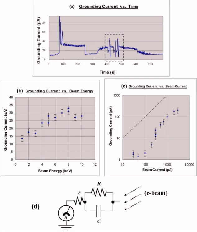
In conjunction with a sensible change of the imaging contrast, a measurable change共approximately a few tens of picoamperes兲 of the grounding current was also detected upon the touchdown of the probe onto the calibrating pattern, as illustrated in Fig. 5共a兲. In contrast to the overshooting spike upon the first touchdown, the second one depicts a much smoother rising of the grounding current. What made the difference is just a little practice of moving the probe while the grounding current is being monitored. This dem-onstrates the need for a quantitative way of determining the contact in a real-time fashion. As for the measured results, we noticed 关by comparing Figs. 3共c兲 and 5共b兲兴 that the change of the steady-state grounding current seems to in-crease upon the reduction of the imaged area, which may not be comprehensible at a glance. This observation addresses the issue of what factors determine the magnitude of the change in the steady-state grounding current upon the event of touchdown. Among the significant factors we have veri-fied experimentally are the energy and the flux of the elec-tron beam. As shown in Figs. 5共b兲 and 5共c兲, we have ob-served a monotonically linear behavior for the overall relation between the steady-state grounding current and ei-ther factor. It remains to be a subject of furei-ther study about how exactly these characteristics are related to the underly-ing causes such as the surface properties.
IV. DISCUSSION
As demonstrated in the previous section, our methods to detect the contact of probes can be carried out in both quali-tative and quantiquali-tative fashions. Being aware of the rapidly growing community associated with SEM-based multiprobe systems, we are convinced that the quantitative method to determine the contact 共in terms of the grounding current兲 may help some standard procedures to be established. As a result, different measurements with SEM-based multiprobe systems can be more reliable for comparison.
On the other hand, our method of mapping the contact sites can be interpreted as the tracking of the invisible con-tact spots by the extension of the imaging contrast along conductive lines. Remarkably, we can also apply the same underlying principle in a reversed fashion. If a contact has been established between the grounded probe and a desig-nated conductive line, the visible discontinuity of the imag-ing contrast along this line will then reveal the failure sites of electrical continuity. This failure mapping technique allows
FIG. 4. A test for our method of mapping the contact point共s兲 with a prac-tical version of the calibrating pattern. SEM images共a兲 and 共b兲 show the sequential touchdown of the probe onto each set of the lines共by moving around both the probe and the calibrating pattern兲, causing a drastic change of the imaging contrast for some line共s兲 to determine the corresponding coordinate of the contact point共s兲. Extrapolated from these “lighted lines” on the calibrating pattern, the corresponding dashed strips indicate the final identification of the possible contacted regions on the probe.共c兲 A summary of the experimental data from six different runs of touchdown in a statistical fashion. Six dashed strips extrapolated from the lighted lines in all events of touchdown are plotted together on the probe. Essentially, three lines of each set coincide with one another very well. The detached calibrating pattern serves as irrelevant background in this image.共d兲 An overview of the cali-brating pattern after six runs of touchdown. Note that the six damaged sites due to the unsatisfactorily rough touchdown of various extents are enclosed by six dashed boxes of various shapes. In particular, the thick dashed square and triangle enclose the contact sites corresponding to the events of共a兲 and 共b兲, respectively.
103709-4 Nien et al. Rev. Sci. Instrum. 77, 103709共2006兲
spatial designation of the desired target to examine, which may provide a timely solution to the ever increasing chal-lenge of failure analysis in the semiconductor industry deal-ing with more and more compact nanoelectronics.9
In our attempt to understand the experimental results in a quantitative manner, we have modeled the imaged sample by assuming an equivalent R-C parallel circuit共i.e., a resistor of resistance R and a capacitor of capacitance C in parallel兲, as depicted in Fig. 5共d兲. A contact resistance r between the probe and the surface is also taken into account. As an
ex-ample of how this model advances our analysis, let us exam-ine the measurement of the steady-state grounding current versus the flux of the electron beam. We assume that the continuous impingement of the electron beam can be re-garded as the driving force 共by establishing a nonuniform spatial distribution of charge across the sample兲 to build up a steady-state bias voltage across the resistor R as well as the capacitor C. In spite of the seemingly complicated mecha-nisms involved in the SEM imaging process, the built steady-state bias voltage is probably related to the flux of the
FIG. 5.共Color online兲 Quantitative analysis of the measured grounding current. 共a兲 The grounding current is plotted as a function of time for the touchdown of the probe onto the calibrating pattern twice. Note that a wild fluctuation in the grounding current occurs whenever a SEM image is being recorded by a slow scan, as highlighted by a dashed box.共b兲 The steady-state grounding current upon contact is recorded as a function of the beam energy in a linear plot. The beam current was set to 300 pA.共c兲 The steady-state grounding current upon contact is recorded as a function of the beam current in a log-log plot. The dashed line corresponds to I共ground兲=I共beam兲. The beam energy was set to 5 keV. In all experiments in 共b兲 and 共c兲, the emission current of the electron source was set to 39A, and the magnification was 1300.共d兲 A proposed model for the imaged sample is composed of an equivalent R-C parallel circuit. A possible contact resistance r between the probe and the surface is also taken into account.
electron beam in a monotonic fashion. If we further assume an ideal case where this monotonic relation can be approxi-mated by a constant proportionality 共i.e., V/I共beam兲⬅k = const兲 within a range of the impinged electron flux, the measurement of the characteristic I-V curve in this range is then equivalent to the measurement of the steady-state grounding current versus the impinged electron flux up to a proportional constant 关i.e., R = V / I共ground兲=k
⫻I共beam兲/I共ground兲 with a constant k for this ideal case兴. Since there can be a background value of the grounding cur-rent that has nothing to do with the contact of the probe with the sample, I共ground兲 in the above formula actually corre-sponds to the “change” in the steady-state grounding current upon the event of touchdown. This background value may be reduced by adjusting the impinged region of the electron beam.
Alternatively speaking, having the continuous impinge-ment of the electron beam to serve as the driving force共in place of an externally applied bias voltage兲, one may be able to characterize the electrical properties of an electrically iso-lated object through the proper contact with a grounded probe, followed by the measurement of the grounding cur-rent as a function of the beam energy and/or flux. Notice that this one-probe approach may become indispensable for nanostructures, as the conventional four-probe electrical measurement is unlikely to be applicable in these cases. On the one hand, there is often limited space on a nanostructure to establish four separate contacts for the conventional ver-sion of the electrical measurement. On the other hand, the surface properties are likely to play a dominant role in the case of a nanostructure, suggesting a possibility to define alternative ways of measuring the electrical properties.
In the one-probe electrical characterization based on our methods, the grounded probe can be viewed to play the role of designating an individual object共among other electrically isolated ones兲 by a local contact for the charging effect to be “turned off.” This is followed by the measurement of the grounding current共through the probe兲 as a function of a pa-rameter of interest to run the electrical characterization共in an unconventional fashion兲 for this designated nanostructure. Therefore, the basic configuration共as depicted in Fig.1兲 we adopted to determine the contact of probes may also allow us to study the electrical properties of individual nanostructures one at a time. Note that the great opportunity of “individual study” is not possible if the grounding current is collected through the sample holder instead,10as we cannot selectively measure the contribution of a specified feature to the ground-ing current in that case. As for the required electrical isola-tion of the surface features from the ground, one may be able to achieve “tenability” by some lithographical designs along with the so-called field effect 共say, by applying a proper “gate voltage”兲.
In comparing the relation between the scanning tunnel-ing microscopy共STM兲 and the scanning tunneling spectros-copy共STS兲,11our one-probe approach to the electrical char-acterization seems more promising for the corresponding technique called “scanning electron spectroscopy共SES兲” to be established in an instrumentally simple fashion. The basic features of SES to be expected include at least one mode of
spectroscopic measurement 共e.g., I-V characteristic兲 with a spatial resolution close to that of SEM. In addition to the energy and the flux of the electron beam as promising inde-pendent variables for this technique, further studies may also find ways for other parameters共e.g., the operated magnifica-tion兲 to join the available SES modes for nanoscale research.
V. SUMMARY
In summary, we have developed simple but effective methods of determining when and where a probe starts to contact an electrically isolated surface. Based on the charg-ing effect common to various kinds of electron microscopy, these techniques are designed for a multiprobe system oper-ated inside a scanning electron microscope共SEM兲. As con-ceptually predicted and experimentally confirmed, a touch-down of an electrically grounded probe leads to an acute change in the imaging contrast of the contacted surface, which also causes a rapid jump of the grounding current 共ranging from a few to tens of picoamperes兲. Thus, the de-tection of contact can be carried out in both qualitative and quantitative manners, providing a basis for establishing rel-evant standard procedures.
In addition, we have achieved the spatial mapping of the contact point共s兲 with respect to the probe itself 共unlike what SPM is restricted兲. This involves a specially designed litho-graphical pattern with two mutually vertical sets of parallel conductive lines. The precision of this mapping technique is simply determined by the pitch of these parallel lines, which can be as small as the capability achievable in e-beam lithog-raphy. Remarkably, one can also apply the reversed working principle to reveal the failure sites of electrical continuity in a complicated circuit. This mapping technique may therefore provide an effective solution to the upcoming challenge of failure analysis for nanoelectronics in the semiconductor industry.
An equivalent R-C parallel circuit was examined to model the imaged sample in our attempt at a quantitative analysis of the experimental results. We have also discussed a possible one-probe version of the electrical characterization based on the same underlying principle, which may turn out to be indispensable for various studies and applications of nanostructures. Further development along this track is promising to realize an instrumentally simple version of scanning electron spectroscopy共SES兲 with various modes. ACKNOWLEDGMENT
This work was supported by the Center of Nano-Science and Technology共CNST兲 of the University System of Taiwan 共UST兲.
1Among comprehensive books to provide an overview is L. Reimer,
Scan-ning Electron Microscopy, Springer Series in Optical Sciences Vol. 45
共Springer, Berlin, 1985兲.
2M.-F. Yu, O. Lourie, M. J. Dyer, K. Moloni, T. F. Kelly, and R. S. Ruoff, Science 287, 637共2000兲.
3T. Kuzumaki, H. Sawada, H. Ichinose, Y. Horiike, and T Kizuka, Appl. Phys. Lett. 79, 4580共2003兲.
4H. W. C. Postma, A. Sellmeijer, and C. Dekker, Adv. Mater.共Weinheim, Ger.兲 12, 1299 共2000兲.
103709-6 Nien et al. Rev. Sci. Instrum. 77, 103709共2006兲
5S.-D. Tzeng, C.-L. Wu, Y.-C. You, T. T. Chen, and S. Gwo, Appl. Phys. Lett. 81, 5042共2002兲.
6K. S. Kim, S. C. Lim, I. B. Lee, K. H. An, D. J. Bae, S. Choi, J.-E. Yoo, and Y. H. Lee, Rev. Sci. Instrum. 74, 4021共2003兲.
7R. Gupta, R. E. Stallcup II, and M. in het Panhuis, Nanotechnology 16, 1707共2005兲.
8S. Tiwari and H. Tokumoto, Report on Japan-US Symposium on Tools and
Methrology for NanoTechnology共Cornell University, Ithaca, 2003兲.
9J. Ouellette, Ind. Phys. 4, 11共1998兲.
10J. Liebault, K. Zarbout, D. Moya-Siesse, J. Bernardini, and G. Moya, Appl. Surf. Sci. 212–213, 809共2003兲.
11Among comprehensive books to provide an overview is: C. J. Chen,
In-troduction to Scanning Tunneling Microscopy, Oxford Series in Optical
and Imaging Sciences Vol. 4共Oxford University Press, New York, 1993兲.