E L S E V I E R Microelectronic Engineering 30 (1996) 157-160
MICROELECTRONIC
ENGINEERING
TiNx AS A N E W E M B E D D E D M A T E R I A L F O R A T T E N U A T E D P H A S E SHIVF
M A S KWen-an Loong, Tzu-ching Chen and Jin-chi Tseng
Institute of Applied Chemistry, National Chiao Tung University, Hsinchu 300, Taiwan, Republic of China
In this paper TiNx (x > 1.3) as a new material suitable for using as an embedded layer for an attenuated phase shift mask (APSM) is presented. TiNx thin film was formed by plasma sputtering under a gas mixture of Ar and Na (40:2 sccm). The related characteristics of TiNx at 365 nm (i-line) wavelength are as follows: n (refractive index) ~3.07; k (absorbance coefficient) ~0.531; R (reflectivity) 27~30%; p (resistivity) - 5 2 pi2-cm (132 nm on quartz). For required phase shift degree 0 =180 °, calculated thickness d of TiNx film is 88.2 nm, and transmittance T under 365 nm wavelength at this thickness is 14.5 % which is within the useful range for APSM. TiNx film also has good electrical conductivity, suitable for e-beam direct-write in patterning mask.
1. Introduction
Using embedded monolayer as both absorptive layer and phase shifter for the fabrication of an attenuated phase shift mask (APSM) has attracted industry attention recently due to the fact that the embedded APSM has the merits of easier fabrication, inspection and repair than other types of PSM. There are two major drawbacks in some reported absorptive shifters. Firstly, absorptive shifters such as Cr-O, Mo-Si-O based materials, do not have the conductivity in the condition as the shifter, therefore, a thin Mo or other metal film must be coated on the shifter t o prevent the charging effect during e-beam writing on the mask [1]. Secondly, optical transmissions of absorptive shifters such as Si-N based materials, are difficult to control. The transmissions usually are too high at visible wavelength, causing the mask's alignment by laser beam during stepper exposure more difficult [2].
In this paper TiNx (x >1.3) as a new material suitable for using as an embedded layer for APSM is presented. The TiNx film has a low transmi- ttance (<30%) at visible wavelength. The TiNx film also has good electrical conductivity, suitable for e-beam direct-write in patterning mask. The R- T method [3] and related optical equations [2] were
used to obtain the refractive index n and absorbance (or extinction ) coefficient k.
2. Experimental
The deposition of TiNx thin films on substrates of quartz or Si wafer were carried out with an Ion Tech Microvac 450cb sputtering system. The sputtering conditions were as follows: reaction pressure 8.0 x 10 -3 torr; target Titanium; input gas mixture At/N2=40/2 scorn; substrate: glass, quartz or Si wafer; RF forward 250 W; RF reverse 8.4 W; DC bias -145 V; deposition rate 0.11-4).18 ~/sec. Transmittance and reflectivity were taken from a Hitachi U-3501 double beam UV-VIS-NIR spectrophotometer. Thicknesses were measured from a Dektak 3030 surface profilometer and a Rudolph Research auto EL II ellipsometer. Depth profiles of ion were analyzed by a Cameca IMS-5F Secondary Ion Mass Spectrometer (SIMS) using 02 + as ion source under 12.5kV and 3000 mass resolution power. Resistance measurements were performed using a Napson RT-7 resistivity analyzer. Micrographs were taken by a Hitachi S-4000 field emission SEM. Atomic force microscope (AFM) used is Digital Nano Scope 3. The composition of TiN was analyzed by Rutherford Backscattering Spectrometry (RIBS) under 2 MeV 4He + and 160 ° 0167-9317/96/$15.00 © 1996 - Elsevier Science B.V. All rights reserved.
158 W-a. Loong et al. /Microelectronic Engineering 30 (1996) 157-160 scattering angle.
3. Results and Discussion
TiNx on quartz was formed by plasma sputtering under a gas mixture of Ar and N2. The different flow ratios o f At:N2 were tested. The results are shown in Table 1. A m o n g the various ratios, TiNx films made from the ratio of 40:2 showed lower reflectivity and also lower resistivity which are critical as an embedded layer in APSM. The depositions of TiNx fabricated with this ratio only were therefore used in this study.
The plot o f reflectivity (R%) of TiNx film vs. wavelength measured directly from a spectrometer is shown in Fig. 1. R% varied from different samples under similar sputtering conditions. A n average of 2 7 - 3 0 % was found. The transmittance T% against wavelength is illustrated in Fig. 2.
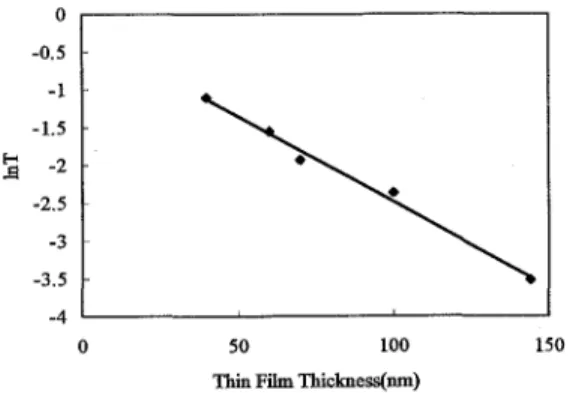
The linearity of In T as a function of TiNx film thickness d is shown in Fig. 3. F r o m this linearity, the absorbance coefficient k is calculated (eq. 1). R% can also be calculated by eq. 1, however, calculated R showed some difference with measured R. The measured R is more reliable and is used in this paper. With known R and k, the refractive index n then can be found (eq. 2). The thickness d of TiNx film required for having 180 ° phase shift was then calculated with known n (eq. 3). From the plot in Fig. 3, the T% at thickness d was determined.
The equations used are listed as follows: In T =(-47tk/%)d + In ( l - R ) ... eq. 1 R=[(n-1)2+k2]/[(n+l)2+k 2] ... eq. 2 d = )~/2(n-1) ... eq. 3 The optical and related characteristics of TiNx at 365 nm (i-line) wavelength are summarized as follows: R% (reflectivity) 27-30%; k (absorbance c o e f f i c i e n t ) - 0 . 5 3 1 ; n (refractive i n d e x ) - 3 . 0 7 ; p (electrical resistivity) - 5 2 Bg2-cm;. calculated thickness d of TiNx film is 88.2 nm to have phase shift degree 0 =180 °, transmittance T% under 365 nm wavelength at this thickness is 14.5. T% is within the useful range for APSM.
With the increased flow rate of nitrogen At/nitrogen mixture, the refractive index n is fou~ to decrease slightly, while k increased according~ The flow rate ratios o f A s / N 2 from 20:2 to 40:2 found to be acceptable for the deposition of Tit film which is suitable to be used as an embedd absorptive shifter. The wide latitude of flow rz makes the control of TiNx properties much easier. The depth profiles of ions of TiNx analyzed 1 SIMS is shown in Fig. 4. Some impurity of oxyg, was found. However, since standard TiN sample not available, the composition of TiNx can n o t determined. RIBS was then tried.
The difficulty of taking RIBS spectrum for th TiNx film on quartz was faced. A n alternati method was used to estimate the ratio of Ti and i A N300 nm thick TiN film on Si wafer w prepared and a sheet resistance Rs o f - 2 . 1 D,/D w measured. The RBS analysis indicated that t] composition of TiN is T i : N = I : I . 3 . The calculat, resistivity p of this TIN1.3 film is ~28 pI2-cm - 1 3 2 nm thickness.
It is quite well known that the increase of N TiN composition will increase its resistivity. ! average electrical resistivity p o f - 5 2 B£2-cm - 1 3 2 nm thickness on quartz was measured f TiNx. By comparing 52 $xf2-cm from TiNx with ' Bg2-cm from TIN1.3 at same thickness, it indicat that the x>l.3 in TiNx. More work is needed f the determination of exact composition of this Ti~ film deposited on quartz.
A SEM of the surface o f TiNx is shown in Fi 5. The crosssectional profile of TiNx is shown Fig. 6. The grain size is considered to be uniform. The A F M roughness analysis o f TiNx is shown Fig. 7. The maximal roughness is about 7.3 n with total thickness of ~132 nm. The 5.5% roughness is resonable for sputtering depositio The effect of this roughness on the degree of pha shift is estimated as 9 - 1 0 ° which is within tolerab range.
The fabrication o f an A P S M using this Tib film has not yet been tried. One drawback of th film is its relatively lower resistance to strong ac or base. The optimization o f wet etching f making the APSM using this material is al~ needed.
W-a. Loong et al. /Microelectronic Engineering 30 (1996) 157-160 Table 1 The effects of flow ratios of At:N2
Flow Ratio At:N2 (sccm) Pressure (mtorr) Film Thickness (nm) Refiectivity (%) Transmittance (%) 10:40 7.6 130 19.3 20:40 7.6 130 17.2 15:15 7.6 120 20.6 16:8 16:4 20:2 40:2 7.6 119 21.2 12.6 9.0 11.7 5,8 Resistivity (mg2-cm) >5.2 >5.2 3.3 0.46 7.6 7.6 7.6 144 126 132 30.5 23.9 19.1 3.0 6.1 6.9 0.043 0.05 0.052 159 168.8 z l l J ~ ' ~ ' . ~ ' '4o~'.~s ' ' 4 ~ ' . ~ ' '~'8~'.~' ' ~ R ' . ~ ' ' 6 ~ ' . ~ ' ' ' 3 4 0 . 9 8 G 5 0 . 0 8 h i l l laO.B- . . . i M ' . o ¢ , ' ' ,~eB'.e~ ' " / , m ' . m ( r i m )
Fig. 1. The plot of reflectivity R vs. Wavelength. Fig. 2. The transmittance T% against wavelength.
[-~ 0 -0.5 - t -1.5 -2 -2.5 -3 -3.5 -4 0 i t 50 100 150
Thin Film Thickness(rim)
1000O0000 10000000 1000000 I 0 0 0 0 0 10000 "~ 1 0 0 0 8 loo 10 1
iiiiiiii;iiiii;iiiiiiiiii?!!!!!!iii!ii!ii ii!ii!: !
TimeTiNx SIMS Profile for Ti, Si, N and O
Fig. 3. The linearity of lnT as a function of TiNx film thickness.
Fig. 4. The depth profiles of ions of TiNx analyzed
by SIMS.
160 W-a. Loong et al. Microelectronic Engineering 30 (1996) 157-160
Fig. 5 The SEM of surface of TiNx. Fig. 6. The crossseetional profile of TiNx.
[ C u r s o r N s r k e r S p = ~ t r u ~ ~ o ~ C e n t e r L i n e O t ' l ~ e t C l z a r S e c t l o n A n a l y s i s t" /-.-~ - \ , j ., . . . . , i m s ~ c ~ r u ~ ~C iqln H e r i z " ~ i s ~ e r ~ e ~ ) 1 0 2 , ~ 4 r.~ H o r i z a i ~ t ~ o e Uert d i s ~ a e l:innl e lea l i n e : o t ' r Q~'fset: ¢rl" I I ~ a k S u r f a c e ~ - e a ~ i t l i r a I ~ r o s s i n , l $ t o p b ~ d ~ e ~ u l e g l e i r R o u g h n e s s A n a l y s i s
Fig. 7. The AFM roughness analysis of TiNx.
4. Conclusions
The flow rate ratios of Ar/N2 from 20:2 to 40:2 ar believed to be acceptable for the deposition of TiN: film which is suitable to be used as an embedde, absorptive shifter. Besides the optical propertie., the relative low resistivity of this TiNx film as a~ absorptive shifter on quartz is another advantage fo e-beam direct-write to reduce the charging effe¢ during mask patterning. More work is needed fo the fabrication of an APSM using this TiNx film t, verify its usefulness.
5. References
1. M. Nakajima et al., SPIE, Vol. 2197, 111 (1994) 2. K. K. Shih and D. B. Dove, J. Vac. Sci. Technol.
B12(l), 32 (1994).
3. T. C. Panlick, Applied Optics, Vol 25(4), 562 (1986).