Volume 2013, Article ID 431614,7pages http://dx.doi.org/10.1155/2013/431614
Research Article
Surface Passivation and Antireflection Behavior of ALD TiO
2
on
n-Type Silicon for Solar Cells
Ing-Song Yu,
1Yu-Wun Wang,
2Hsyi-En Cheng,
2Zu-Po Yang,
3and Chun-Tin Lin
31Department of Materials Science and Engineering, National Dong Hwa University, Hualien 97401, Taiwan
2Department of Electro-Optical Engineering, Southern Taiwan University of Science and Technology, Tainan 710, Taiwan 3Institute of Photonic System, National Chiao Tung University, Tainan 71150, Taiwan
Correspondence should be addressed to Ing-Song Yu; [email protected] Received 16 September 2013; Accepted 30 October 2013
Academic Editor: Jimmy Yu
Copyright © 2013 Ing-Song Yu et al. This is an open access article distributed under the Creative Commons Attribution License, which permits unrestricted use, distribution, and reproduction in any medium, provided the original work is properly cited. Atomic layer deposition, a method of excellent step coverage and conformal deposition, was used to deposit TiO2thin films for the surface passivation and antireflection coating of silicon solar cells. TiO2thin films deposited at different temperatures (200∘C, 300∘C, 400∘C, and 500∘C) on FZ n-type silicon wafers are in the thickness of 66.4 nm± 1.1 nm and in the form of self-limiting growth. For the properties of surface passivation, Si surface is effectively passivated by the 200∘C deposition TiO2thin film. Its effective minority carrier lifetime, measured by the photoconductance decay method, is improved 133% at the injection level of 1 × 1015cm−3. Depending on different deposition parameters and annealing processes, we can control the crystallinity of TiO
2 and find low-temperature TiO2phase (anatase) better passivation performance than the high-temperature one (rutile), which is consistent with the results of work function measured by Kelvin probe. In addition, TiO2thin films on polished Si wafer serve as good ARC layers with refractive index between 2.13 and 2.44 at 632.8 nm. Weighted average reflectance at AM1.5G reduces more than half after the deposition of TiO2. Finally, surface passivation and antireflection properties of TiO2are stable after the cofire process of conventional crystalline Si solar cells.
1. Introduction
Most commercially available solar cells are from silicon, and p-type crystalline silicon solar cells are the mainstream now. In order to increase the efficiency of crystalline silicon solar cells, people in industry try to find the better integration processes of conventional solar cells, to improve the quality of materials, and to cost down the fabrication. Besides, new structures of silicon solar cells with higher efficiency are studied. Passivated emitter and rear, locally diffused cell (PERL), proposed by University of New South Wales, Australia, in 1994, is also one of the designs, which performs
very high efficiency up to 25% [1]. In industry, the conversion
efficiency of 6 inch× 6 inch p-type crystalline silicon solar
cells can be over 20% using the surface passivation technology
with Al2O3 thin films [2]. Unfortunately, the light induced
degradation (LID) makes p-type crystalline silicon solar cells drop around 1% efficiency due to the formation of
boron-oxygen clusters after light exposure [3]. Therefore, PERL
with n-type silicon wafers attracts researchers’ great attention recently and will dominate the crystalline Si solar cell in the
near future [4,5].
For the surface passivation and antireflection coating of
p-type Si solar cells, amorphous SiN𝑥films deposed by the
technique of plasma-enhanced chemical vapor deposition
(PECVD) were well developed in the early 1990s. SiN𝑥thin
films can reduce surface recombination and light reflection and additionally provide very efficient passivation for bulk
defects of low cost Si materials [6, 7]. However, for the
p-type diffused surface of n-p-type Si solar cells, SiN𝑥dielectric
coatings are not suitable for passivation, because its positive charge will decrease the properties of surface passivation. Thermal silicon oxide could be good for passivation
ini-tially, but the Si-SiO2 interface on boron-diffused and
un-diffused surfaces degrades slowly over three months at room
temperature [8, 9]. Besides, amorphous silicon (a-Si) and
Al2O3 are good passivation layers but are not suitable for
oxide (TiO2) reattracts researchers’ attentions, which has been used in the photovoltaic industry as an antireflection coating for many years since the 1980s due to its low growth temperature, a nontoxic and noncorrosive liquid precursor, excellent chemical resistance, an optimal reflective index, and low absorbance at wavelengths relevant to silicon solar cells.
Surface passivation properties of spray pyrolysis TiO2 on
silicon wafer were enhanced by the formation of a SiO2layer
at TiO2/Si interface after being annealed at 950∘C without
degradation [10,11]. Nonstoichiometric TiO𝑥films grown by
pulsed laser deposition (PLD) had some degree of passivation for nondiffused p-type Si surface through the substrate placed
at the edge of plasma [12]. Recently, Thomson et al. proposed
that the TiO2thin films deposited by atmospheric pressure
chemical vapor deposition (APCVD) can effectively passivate n-type silicon and Boron-diffused surfaces as better as the
passivation performance of SiO2. These films were annealed
at 300∘C in N2ambient and light soaked by halogen lamp to
create negative charges for better surface passivation [8].
Many technologies can be employed to grow TiO2thin
films, such as PECVD, APCVD, PLD, spray pyrolysis, reactive
sputtering, and sol-gel [13]. In this paper, we grew TiO2thin
films on Si wafers by atomic layer deposition (ALD) which performs excellent uniformity, accurate thickness control,
and almost 100% step coverage on substrate surface [14].
Some characterization of TiO2 thin films by ALD will be
shown. An investigation of the surface passivation and antire-flection coating on silicon relative to the growth temperatures of ALD will be discussed. The degradation and influence of cofire process for the metallization of Si solar cells will also be studied. This work is essential for the applications of ALD
TiO2thin films in n-type crystalline silicon solar cells.
2. Experiment
In the experiment, we used n-type double-polished FZ silicon
wafers with resistivity 1000Ω-cm, thickness 500 𝜇m, and
orientation (100). Before the deposition of TiO2, the cleanness
of Si wafers was conducted by acetone to remove the organics and 5% hydrofluoric acid to remove the native oxide. Then,
wafer was rinsed in deionized water and dried with N2
gas. Right after the cleaning, Si substrate was placed in the reaction chamber of our ALD system which is shown in
Figure 1. Until the base pressure of chamber reached 2 ×
10−2 torr, we set the deposition temperature as 200∘C, 300∘C,
400∘C, and 500∘C, respectively. For the deposition process of
TiO2 thin films, we employed TiCl4 and H2O as reactants
and Ar (99.999%) as purging gas. The injection volume of
TiCl4and H2O was 0.10 cc and 0.06 cc, respectively, for each
step according to the ideal gas law. One cycle of a monolayer
deposition included eight steps (TiCl4reactant, pump-down,
Ar purge, pump-down, H2O reactant, pump-down, Ar purge,
and pump-down), and it took eight seconds. After 1000-cycle deposition and cool-down to room temperature of the
chamber, n-type FZ Si wafer with double-side TiO2coating
was done for further analysis [15]. First, the characterization
of TiO2 films was made by scanning electron microscopy
(SEM) and X-ray diffraction (XRD). Second, the study of
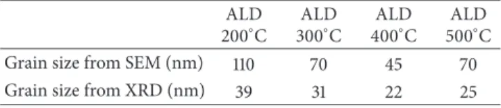
Table 1: Estimation of grain size of TiO2 thin films by SEM and XRD. ALD 200∘C ALD 300∘C ALD 400∘C ALD 500∘C Grain size from SEM (nm) 110 70 45 70 Grain size from XRD (nm) 39 31 22 25
surface passivation for ALD TiO2on n-type FZ silicon wafers
was carried out by Sinton’s quasi-steady-state photoconduc-tance (QSSPC) method and Kelvin probe for work function
measurement [16, 17]. Finally, optical properties of TiO2
thin films were decided by the spectroscopic ellipsometry measurement and reflection spectroscopy in the wavelength range of 300 nm–1200 nm.
3. Results and Discussions
3.1. The Characterization of ALD TiO2 Thin Films. The
surface morphology and cross-section of our TiO2 thin
films were observed by a JSM-6700F SEM with accelerating
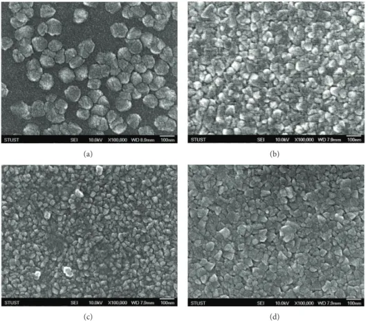
voltage 10 kV. In Figure 2, SEM images of TiO2 thin films
deposited at different temperatures show that these films are polycrystalline and have grain sizes in the range of 45 nm and
110 nm. Cross-section SEM images, in the inset ofFigure 3,
were used to decide the thickness of TiO2 thin films. The
thickness of TiO2thin films is 66.4 nm± 1.1 nm for all growth
temperatures shown inFigure 3. Here, we can find that the
growth rate is independent of the substrate’s temperature, which indicates that the reaction is self-limited by the saturated surface adsorption of reactants. The adsorption thickness, 0.066 nm, is almost the same for each cycle of ALD process. Our ALD system demonstrates very large growth
windows for the TiO2thin films deposited on Si wafers.
The crystallinity of ALD TiO2 thin films at different
temperatures was studied by Bruker X-ray diffractometry. InFigure 4, XRD patterns demonstrate that TiO2thin films deposited at low temperatures are primarily with anatase
phase. As the deposition temperature increased up to 500∘C,
rutile phase began to be obtained in TiO2thin films. When
the TiO2 films are annealed with the parameter of 900∘C,
60 seconds, and O2 ambient, rutile phase dominated in
the films. Rapid thermal annealing (RTA) induces phase
transformation of TiO2films from low-temperature anatase
phase to high-temperature rutile phase. The higher RTA temperature is, the more rutile phase we observe. From this
work, we can control the phase of TiO2 thin films for the
following studies of surface passivation and antireflection coating on n-type Si.
In addition, grain size of ALD TiO2 can be estimated
by SEM images and Scherrer equation of XRD, which is
summarized inTable 1. We get smaller grain size by XRD than
the one by SEM, but their trends are the same at different
deposition temperatures. For TiO2 films only with anatase
phase (at deposition temperatures 200∘C, 300∘C, and 400∘C),
the lower deposition temperature we set, the larger grain size
we observe. According to the growth mechanism of TiO2thin
Chamber TiCl4 H2O Ar Val.1 Val.2 Val.3 Val.4 Val.7 Waste gas treatment Automatic Pressure gauge Manual valve Pump MFC
Figure 1: Schematic of the ALD system.
(a) (b)
(c) (d)
200 300 400 500 0.00 0.02 0.04 0.06 0.08 G ro w th ra te (nm/c yc le) Deposition temperature (∘C)
Figure 3: ALD TiO2 growth rate at temperature 200∘C, 300∘C, 400∘C, and 500∘C is 0.066 nm per cycle due to self-limiting growth. Inset is the cross-section SEM image.
15 20 25 30 35 40 45 50 55 60 A(101) R(211) R(101) ALD200∘C ALD300∘C ALD400∘C ALD500∘C RTA900∘C ALD500∘C R(110) R: rutile A: anatse In te n si ty (a.u .) 2𝜃 (deg)
Figure 4: XRD patterns of TiO2 thin films deposited at 200∘C, 300∘C, 400∘C, 500∘C, and RTA 900∘C.
grain refinement, due to an increased density of sites for
nucleation of crystallization [18]. As the deposition
tempera-ture increases up to 500∘C, we find the phase transformation
to rutile and the effect of grain growth, which could influence
the surface passivation of TiO2thin film on n-type Si.
3.2. Surface Passivation Properties of ALD TiO2. Sinton’s
WCT-120, a photoconductance decay method, was employed to measure the effective minority carrier lifetime of samples.
The effective lifetime (𝜏eff) is a combination of bulk lifetime
(𝜏bulk) and surface lifetime (𝜏sur) as follows:
1 𝜏eff = 1 𝜏bulk + 1 𝜏sur , 1 𝜏sur =2𝑆 𝑊, (1)
where𝑊 is the sample thickness and 𝑆 is surface
recombi-nation velocity. In order to study the surface passivation of
ALD TiO2thin films, we used FZ n-type Si substrate which
5E + 014 1.5E + 015 2E + 015 0 5 10 15 20 25 30 35 40 Eff ec ti ve lif etime ( 𝜇 s)
Minority carrier density (cm−3)
ALD200∘C (21.5 𝜇s) ALD300∘C (11.5 𝜇s) ALD400∘C (9.2 𝜇s) ALD500∘C (5.5 𝜇s) FZ wafer (9.2 𝜇s) 1E + 015
Figure 5: Effective minority carrier lifetime as function of carrier density at different deposition temperatures and their lifetime values at injection level 1× 1015cm−3.
has very large bulk lifetime. Therefore, the effective lifetime measured is close to surface lifetime to calculate the surface
recombination velocity.Figure 5shows the effective lifetime
as function of minority carrier density by WCT-120. The
effective lifetime without ALD TiO2 passivation is 9.2𝜇s at
the injection level of 1× 1015cm−3(𝑆 = 2717 cm/s). After the
deposition of TiO2at 200∘C, the effective lifetime is 21.5𝜇s
at the injection level of 1× 1015cm−3 (𝑆 = 1163 cm/s). Si
surface is effectively passivated by the ALD TiO2thin films,
especially for the one deposited at the low temperature. At
the deposition temperature 500∘C, when rutile phase can be
observed, the degree of surface passivation does not exist
anymore. For the samples with RTA 900∘C, their effective
lifetimes are very low (not shown). From the results of the
effective lifetime measurement, we can find that TiO2 thin
film deposited at 200∘C has the best performance for surface
passivation on n-type Si.
Moreover, we study the degradation and influence of
metallization process in crystalline solar cells. InFigure 6,
the effective lifetime of 30 nm TiO2 thin film grown at
temperature 200∘C slightly increased after five months of
deposition. After cofire process of belt-type furnace at peak
temperature 800∘C, the effective lifetime decreased a little
but is still good enough for surface passivation. We can
summarize that ALD TiO2thin films have high stability for
the applications in crystalline silicon solar cells.
In the study of solar cells, work function is sensitive to the voltage across the barrier of p-n junction and the surface traps in the passivation emitter interface. In this work, nonscanning ambient Kelvin probe, KP 020, was used to
measure the work function of TiO2 thin films at different
deposition temperatures. InFigure 7, the higher deposition
temperature we use, the larger work function of TiO2 we
100 90 80 70 60 50 40 30 20 10 0
Minority carrier density (cm−3)
ALD200∘C (after deposition)15.7 𝜇s
ALD200∘C (after five months)17.8 𝜇s
ALD200∘C (after cofire)16.6 𝜇s
Eff ec ti ve lif etime ( 𝜇 s) 5E + 014 1E + 015 1.5E + 015 2E + 015
Figure 6: Effective minority carrier lifetime of 30 nm TiO2 thin films deposited at 200∘C in three cases: after deposition, five months, and cofire. 200 300 400 500 0 5 10 15 20 25 30 5400 5200 5000 4800 4600 4400 4200 W o rk f u nc tio n (meV) Eff ec ti ve lif etime ( 𝜇 s) Deposition temperature (∘C)
Figure 7: Work function (◼) and effective lifetime () of TiO2thin films at different deposition temperatures.
lifetimes at different deposition temperatures. To explain this,
we can see the energy band diagram of TiO2 and Si in
Figure 8. TiO2/Si heterojunction makes energy band bending
at the interface of TiO2and n-type Si [19]. According to the
work function of TiO2 thin films we measured, more band
bending occurred in the case of TiO2film deposited at 500∘C,
which induce more recombination at the interface and lower effective lifetime of samples.
3.3. Optical Properties of ALD TiO2. Now we will
demon-strate that our ALD TiO2thin films are an excellent
antire-flection coating layer for crystalline silicon solar cells. For the conventional quarter-wavelength antireflection coating (ARC), the refractive index of coating layer has to be chosen
as √𝑛𝑠, where 𝑛𝑠 is the refractive index of substrate, that
is, Si in this case. For example, considering the refractive
index of Si in the spectral ranges of 400 nm–800 nm [20], the
refractive index of quarter-wavelength ARC thin films should
be in the range of∼2.36–1.92. To verify this, we performed the
spectroscopic ellipsometry measurements and extracted the
refractive index of our ALD TiO2thin films.Figure 9shows
the refractive index as function of wavelength for our TiO2
thin film deposited at temperature 200∘C. Its refractive index
decreases monotonically from 2.65 to 2.25 as wavelength decreases from 375 nm to 900 nm, showing a similar trend as
anatase-phase bulk TiO2[21] but having a little lower value
of index, which probably is because of polycrystal structure
in our films (see SEM images inFigure 2). Most importantly,
the results show that our ALD TiO2thin films are an excellent
choice of quarter-wavelength ARC layer for Si solar cells. To further prove this, we used Hitachi U-4100 to measure
the reflectance spectra of our ALD TiO2 thin films and a Si
wafer as a reference, shown inFigure 10. Firstly, all of TiO2
deposited Si wafers show a much lower reflectance than those of a bare Si wafer over the measured spectral range. Secondly,
a minimum reflectance of TiO2deposed Si wafers is observed
at∼550 nm, which is consistent with the requirement of film
thickness for quarter-wavelength ARC; that is,𝑑 = 𝜆/4𝑛TiO2.
Taking𝜆 = 550 nm and 𝑛TiO2 ≈ 2.15, we have 𝑑 = 64 nm,
which agrees with our SEM results. Again, this indicates
that our TiO2thin films serve as an ARC layer. Thirdly, the
reflectance of all TiO2deposited Si increases monotonically
from∼550 nm to ∼1000 nm. This is because the thickness
(66.4 nm) of our TiO2film deviates the𝑑 = 𝜆/4𝑛TiO2 further
and further as wavelength increases. Fourthly, a bump rising at around 1000 nm is observed for all samples. This is because the reflectance from Si backside surface starts to contribute the measured reflectance as wavelength approaching the band gap wavelength of Si.
To overall justify the ARC performance of our TiO2
thin films for solar cells, we calculate the weight average reflectance (WAR) at AM1.5G in the range of 300 nm to
1200 nm. The results show that all of our ALD TiO2 thin
films have WAR (16.68%–18.92%) less than the half of WAR
(38.36%) of bare Si. The TiO2 thin film grown at 200∘C
shows the lowest value of WAR because it has the lowest refractive index deduced from ellipsometry. A lower WAR value can be achieved with optimized growth conditions and film thickness. Moreover, the reflectance spectra as well as the WAR are almost the same after cofire process by
belt-type furnace at peak temperature 800∘C (not shown), which
indicates that our ALD TiO2 thin films are suitable for the
fabrication processes of crystalline silicon solar cells.
4. Conclusion
Growth window of self-limiting can be from 200∘C to 500∘C
in our TiO2 ALD system with the growth rate 0.066 nm
per cycle. All these films are excellent antireflection coating
layers for Si. For lower deposition temperature of TiO2thin
films, we find smaller energy band bending in the interface of
TiO2/Si and better surface passivation performance. The best
surface passivation and antireflection coating on Si wafers
VB CB Si Si CB VB ALD200∘CEF ALD500∘CEF EF TiO2 TiO2 Contact EF EC EV q𝜒 = 4.2 eV q𝜒 = 4.05 eV
Figure 8: The left hand side is energy band diagrams of TiO2and Si before contact. After contact, band bending occurs at the interface of TiO2and Si.
300 400 500 600 700 800 900 2.10 2.15 2.20 2.25 2.30 2.35 2.40 2.45 2.50 2.55 2.60 2.65 2.70 Ref rac ti ve index Wavelength (nm) ALD200∘C
Figure 9: Refractive index as function of wavelength for TiO2thin film grown at 200∘C. 200 400 600 800 1000 1200 0 10 20 30 40 50 60 70 80 90 100 Reflec ta n ce (%) Wavelength (nm) FZ wafer (WAR38.36%) ALD200∘C (WAR16.68%) ALD300∘C (WAR17.38%) ALD400∘C (WAR18.92%) ALD500∘C (WAR18.67%)
Figure 10: Reflectance of bare Si wafer and Si with TiO2thin films grown at different temperatures as function of wavelength from 300 nm to 1200 nm.
anatase phase in TiO2film. Once the rutile appears via
high-temperature depositions or annealing processes, the degree of surface passivation will not exist. After the cofire process of conventional crystalline Si solar cells, we prove that their surface passivation and antireflection properties are very stable, which can be applied for n-type crystalline silicon solar cells.
Conflict of Interests
The authors declare that there is no conflict of interests regarding the publication of this paper.
Acknowledgments
The authors acknowledge National Science Council of Taiwan (NSC 101-2218-E-259-001) for financially supporting this study and E-Ton Solar Tech. Co., Ltd., for the measurement of Sinton WCT-120 and Hitachi U-4100.
References
[1] M. A. Green, J. Zhao, and A. Wang, “23% module and other sili-con solar cell advances,” in Proceedings of 2nd World Conference
on Photovoltaic Energy Conversion, vol. 1187, 1998.
[2] F. Werner, B. Veith, V. Tiba et al., “Very low surface recombina-tion velocities on p—and n-type c-Si by ultrafast spatial atomic layer deposition of aluminum oxide,” Applied Physics Letters, vol. 97, no. 16, Article ID 162103, 2010.
[3] K. Bothe, R. Sinton, and J. Schmidt, “Fundamental boron-oxygen-related carrier lifetime limit in mono- and multicrys-talline silicon,” Progress in Photovoltaics, vol. 13, no. 4, pp. 287– 296, 2005.
[4] J. Zhao and A. Wang, “Rear emitter n-type passivated emitter, rear totally diffused silicon solar cell Structure,” Applied Physics
Letters, vol. 88, no. 24, Article ID 242102, 2006.
[5] B. G. Lee, J. Skarp, V. Malinen, S. Li, S. Choi, and H. M. Branz, “Excellent passivation and low reflectivity Al2O3/TiO2bilayer coating for n-wafer silicon solar cells,” in Proceedings of 38th
IEEE Photovoltaic Specialists Conference (PVSC ’12), 2012.
[6] A. G. Aberle, “Surface passivation of crystalline silicon solar cells: a review,” Progress in Photovoltaics, vol. 8, pp. 473–487, 2000.
[7] E. Fourmond, G. Dennler, R. Monna, M. Lemiti, A. Fave, and A. Laugier, “UVCVD silicon nitride passivation and ARC layers
for multicrystalline solar cells,” Solar Energy Materials and Solar
Cells, vol. 65, no. 1, pp. 297–301, 2001.
[8] A. F. Thomson, S. Z. Lynn, and K. R. McIntosh, “Passivation of silicon by negatively charged TiO2,” in Proceedings of 25th
European Photovoltaic Solar Energy Conference and Exhibition (EUPVSEC ’05), vol. 1146, 2010.
[9] A. F. Thomson and K. R. Mclntosh, “Degradation of oxide-passivated boron-diffused silicon,” Applied Physics Letters, vol. 95, Article ID 052101, 2009.
[10] B. S. Richards, J. E. Cotter, and C. B. Honsberg, “Enhancing the surface passivation of TiO2coated silicon wafers,” Applied
Physics Letters, vol. 80, no. 7, pp. 1123–1125, 2002.
[11] B. S. Richards, “Single-material TiO2double-layer antireflection coatings,” Solar Energy Materials and Solar Cells, vol. 79, no. 3, pp. 369–390, 2003.
[12] L. M. Doeswijk, H. H. C. De Moor, D. H. A. Blank, and H. Rogalla, “Passivating TiO2 coatings for silicon solar cells by pulsed laser deposition,” Applied Physics A, vol. 69, no. 7, pp. S409–S411, 1999.
[13] P. Vitanov, G. Agostinelli, A. Harizanova et al., “Low cost surface passivation for p-type mc-Si based on pseudobinary alloys (Al2O3)𝑥(TiO2)1−𝑥,” Solar Energy Materials and Solar Cells, vol. 90, no. 15, pp. 2489–2495, 2006.
[14] S. M. George, “Atomic layer deposition: an overview,” Chemical
Reviews, vol. 110, no. 1, pp. 111–131, 2010.
[15] H.-E. Cheng, C.-M. Hsu, and Y.-C. Chen, “Substrate materials and deposition temperature dependent growth characteristics and photocatalytic properties of ALD TiO2films,” Journal of the
Electrochemical Society, vol. 156, no. 8, pp. D275–D278, 2009.
[16] A. Cuevas and D. Macdonald, “Measuring and interpreting the lifetime of silicon wafers,” Solar Energy, vol. 76, no. 1–3, pp. 255– 262, 2004.
[17] K. Dirscherl, I. Baikie, G. Forsyth, and A. Van der Heide, “Utilisation of a micro-tip scanning Kelvin probe for non-invasive surface potential mapping of mc-Si solar cells,” Solar
Energy Materials and Solar Cells, vol. 79, no. 4, pp. 485–494,
2003.
[18] D. R. G. Mitchell, D. J. Attard, and G. Triani, “Transmission electron microscopy studies of atomic layer deposition TiO2 films grown on silicon,” Thin Solid Films, vol. 441, no. 1-2, pp. 85–95, 2003.
[19] S. M. Sze and K. K. Ng, Physics of Semiconductor Devices, 2nd edition, 1981.
[20] E. D. Palik, Handbook of Optical Constants of Solids, vol. 1, 1991. [21] G. E. Jellison Jr., L. A. Boatner, J. D. Budai, B.-S. Jeong, and D. P. Norton, “Spectroscopic ellipsometry of thin film and bulk anatase (TiO2),” Journal of Applied Physics, vol. 93, no. 12, pp. 9537–9541, 2003.
Submit your manuscripts at
http://www.hindawi.com
Hindawi Publishing Corporation
http://www.hindawi.com Volume 2014
Inorganic Chemistry International Journal of
http://www.hindawi.com Volume 2014
Hindawi Publishing Corporation
http://www.hindawi.com Volume 2014
Carbohydrate
Chemistry
International Journal ofHindawi Publishing Corporation
http://www.hindawi.com Volume 2014
Journal of
Chemistry
http://www.hindawi.com Volume 2014
Hindawi Publishing Corporation http://www.hindawi.com Analytical Methods in Chemistry Journal of Volume 2014 Bioinorganic Chemistry and Applications Hindawi Publishing Corporation
http://www.hindawi.com Volume 2014
Spectroscopy
International Journal of Hindawi Publishing Corporationhttp://www.hindawi.com Volume 2014
The Scientific
World Journal
Hindawi Publishing Corporationhttp://www.hindawi.com Volume 2014 http://www.hindawi.com Volume 2014
Chromatography Research International Hindawi Publishing Corporation
http://www.hindawi.com Volume 2014
Applied ChemistryJournal of
Hindawi Publishing Corporation
http://www.hindawi.com Volume 2014
Hindawi Publishing Corporation
http://www.hindawi.com Volume 2014 Theoretical Chemistry
Journal of
Hindawi Publishing Corporation
http://www.hindawi.com Volume 2014
Journal of
Spectroscopy
http://www.hindawi.com Volume 2014
Journal of Hindawi Publishing Corporation
http://www.hindawi.com Volume 2014 Quantum Chemistry http://www.hindawi.com Volume 2014
Hindawi Publishing Corporation
http://www.hindawi.com Volume 2014
Catalysts
Journal ofElectrochemistry
International Journal ofHindawi Publishing Corporation