Use of Si + pre-ion-implantation on Si substrate to enhance the strain relaxation of the
Ge x Si 1 x metamorphic buffer layer for the growth of Ge layer on Si substrate
Y. C. Hsieh, E. Y. Chang, G. L. Luo, M. H. Pilkuhn, S. S. Tang, C. Y. Chang, J. Y. Yang, and H. W. Chung
Citation: Applied Physics Letters 90, 083507 (2007); doi: 10.1063/1.2475361 View online: http://dx.doi.org/10.1063/1.2475361
View Table of Contents: http://scitation.aip.org/content/aip/journal/apl/90/8?ver=pdfcov Published by the AIP Publishing
Articles you may be interested in
Photoluminescence and positron annihilation spectroscopy of MeV Si + ion-irradiated Si y O 1 y : Er ( y 1 / 3 ) thin films
J. Appl. Phys. 105, 053517 (2009); 10.1063/1.3086644
Comment on “Use of Si + pre-ion-implantation on Si substrate to enhance the strain relaxation of the Ge x Si 1 x metamorphic buffer layer for the growth of Ge layer on Si substrate” [Appl. Phys. Lett.90, 083507 (2007)]
Appl. Phys. Lett. 93, 156102 (2008); 10.1063/1.3003873 Defects in Ge and Si caused by 1 MeV Si + implantationa) J. Vac. Sci. Technol. B 26, 425 (2008); 10.1116/1.2834557
Role of the Si Si O 2 interface during dopant diffusion in thin silicon on insulator layers J. Appl. Phys. 100, 096112 (2006); 10.1063/1.2374933
Deep level defects in proton radiated GaAs grown on metamorphic Si Ge Si substrates J. Appl. Phys. 100, 034503 (2006); 10.1063/1.2220720
This article is copyrighted as indicated in the article. Reuse of AIP content is subject to the terms at: http://scitation.aip.org/termsconditions. Downloaded to IP: 140.113.38.11 On: Thu, 01 May 2014 00:38:59
Use of Si
+pre-ion-implantation on Si substrate to enhance the strain
relaxation of the Ge
xSi
1−xmetamorphic buffer layer for the growth of Ge
layer on Si substrate
Y. C. Hsieh and E. Y. Changa兲
Department of Materials Science and Engineering, National Chiao-Tung University, Hsin-Chu, 30050 Taiwan, Republic of China
G. L. Luob兲
National Nano Device Laboratories, No 26, Prosperity Road 1, Science-based Industrial Park, Taiwan 300, Republic of China
M. H. Pilkuhn, S. S. Tang, and C. Y. Chang
Department of Materials Science and Engineering, National Chiao-Tung University, Hsin-Chu, 30050 Taiwan, Republic of China
J. Y. Yang and H. W. Chung
National Nano Device Laboratories, No 26, Prosperity Road 1, Science-based Industrial Park, Taiwan 300, Republic of China
共Received 29 September 2006; accepted 14 January 2007; published online 22 February 2007兲 Si+pre-ion-implantation combined with a Ge
xSi1−xmetamorphic buffer structure for the growth of Ge layer on Si substrate is proposed. Enhanced strain relaxation of the GexSi1−xmetamorphic buffer layer on Si substrate was achieved due to the introduction of the point defects by heavy dose Si+ pre-ion-implantation. Because of the strain relaxation enhancement and the interface blocking of the dislocations in the GexSi1−xmetamorphic buffer structure, the total thickness of the buffer layers was only 0.45m. No cross-hatch pattern was observed on the Ge surface and the dislocation density for the top Ge film was only 7.6⫻106cm−2. © 2007 American Institute of Physics.
关DOI:10.1063/1.2475361兴
Due to the higher mobility of its carriers and its narrower band gap as compared to those of silicon 共Si兲, Ge is now emerging as a viable candidate to supplement Si for comple-mentary metal oxide semiconductor devices and 1.3– 1.55m optoelectronics applications.1,2As a result, it is essential to develop methods for the heteroepitaxial growth of Ge on Si. Such growth is not straightforward because of the large lattice mismatch共4%兲 between Ge and Si, which limits the quality of the epitaxial layers grown. After reach-ing a critical thickness, the Ge layer usually contains many misfit and threading dislocations, making it unsuitable for any practical applications.3
This study reports on a high dose Si+ pre-ion-implantation technique which is used to enhance strain relax-ation at the interface between the metamorphic buffer layers and the Si substrate in order to facilitate the growth of a high quality Ge on the Si. The epitaxial structure in this study is illustrated in Fig.1. The composition of the GexSi1−x meta-morphic buffer layers was carefully formulated to block the dislocations in the lower layers. The Ge compositions in the two metamorphic buffer layers were intentionally grown to 80% and 90% each. Because the point defects were intro-duced by a Si+pre-ion-implantation on the surface of the Si substrate, the level of relaxation was enhanced, the thickness of the metamorphic buffer was greatly reduced, and the sur-face morphology was improved. More interestingly, the dis-location density of the top Ge layer was effectively reduced to 106cm−2.
The experiments in this work can be divided into two parts. The first part involves the growth of the GexSi1−x meta-morphic buffer layers on the Si substrates without Si+ ion implantations. The growth of the GexSi1−xand Ge layers was carried out using an ultrahigh vacuum, chemical-vapor depo-sition system with a base pressure of less than 2 ⫻10−8Torr. After RCA cleaning of the 4 in. Si 共100兲 sub-strate surface, a GexSi1−x metamorphic buffer structure,
in-a兲Electronic mail: [email protected] b兲Electronic mail: [email protected]
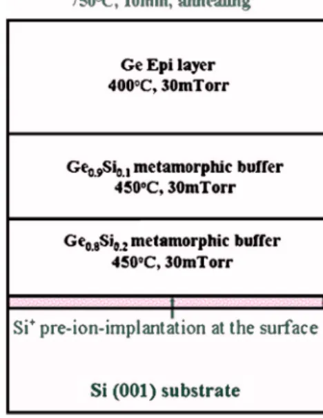
FIG. 1.共Color online兲 Layer structure and the growth conditions for the Ge film grown on the Si substrate with GexSi1−xmetamorphic buffer layers.
Note that GexSi1−xwas grown at two growth rates, the Ge composition set at
80% and 90%, and the Si substrate implanted with high dose Si+ions. APPLIED PHYSICS LETTERS 90, 083507共2007兲
0003-6951/2007/90共8兲/083507/3/$23.00 90, 083507-1 © 2007 American Institute of Physics
This article is copyrighted as indicated in the article. Reuse of AIP content is subject to the terms at: http://scitation.aip.org/termsconditions. Downloaded to IP: 140.113.38.11 On: Thu, 01 May 2014 00:38:59
cluding one Ge0.9Si0.1 layer and one Ge0.8Si0.2 layer, was grown at 430 ° C.3 Then a pure Ge top layer was subse-quently grown at 400 ° C with the same vapor pressure and with a constant GeH4flow rate of 10 SCCM共SCCM denotes cubic centimeter per minute at STP兲. After the Ge growth was finished, in situ annealing at 750 ° C for duration of 15 min was employed to improve the crystalline quality of the epitaxial layers. The optimum thickness of the GexSi1−x metamorphic buffer layer should be larger than 1.45m for strain relaxation to occur so that a high quality pure Ge film can be achieved.3
The second part of this work focuses on the study of the effect of Si+ pre-ion-implantation on the growth of the GexSi1−x metamorphic layer. As mentioned above, the GexSi1−x buffer structure was grown with the same Ge com-position as that of the Si+ implanted Si substrate. The im-plantation involved a Si+dose of 5⫻1015cm−2administered at an acceleration voltage of 50 keV. Figures2共a兲 and2共b兲 show the bright-field, cross-sectional transmission electron microscopy共TEM兲 images of the samples with and without the Si+ pre-ion-implantation, respectively. Figure 2共a兲 was taken by using a diffraction vector g =关004兴, and the surface of the Si substrate was modified with a Si+ pre-ion-implantation. By contrast, Fig. 2共b兲 was taken by using a diffraction vector g =关004兴, and the Si substrate was not im-planted. The top Ge layer and the GexSi1−x metamorphic buffer are clearly shown in both images. In Fig.2共a兲a dark region can be observed at the interface between the GexSi1−x buffer and the Si substrate, this region is associated with the defects induced by the Si+pre-ion-implantation. The thinner buffer layers were observed in the GexSi1−x metamorphic buffer layers with a pre-ion-implantation, and the optimized
thickness of the GexSi1−x metamorphic buffer required for the growth of a high quality Ge film was only 0.45m. By contrast, in Fig.2共b兲, in order to obtain a high-quality Ge top layer, a thicker metamorphic buffer layer was required to relax the strain energy for the sample without pre-ion-implantation. In this case, the optimized thickness of the GexSi1−xmetamorphic buffer for the growth of high quality Ge film was larger than 1.45m.
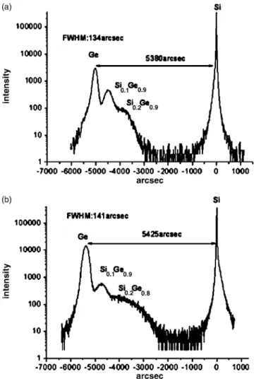
In Fig. 3共a兲, the single crystalline peak for the top Ge layer共Ge兲 is clearly visible with a strong intensity. It sepa-rated from the Si substrate peak 共Si兲 with a distance of
Si-Ge= 5380 arc sec, which indicates that the top Ge layer is close to full relaxation共in case of full relaxation,Si-Ge = 5366 arc sec兲. Other smaller additional peaks are shown on the right side of the Ge peak. These smaller peaks corre-spond to the different GexSi1−x layers in the metamorphic buffer. Because the Ge composition in the buffer begins at x = 0.8共rather than at x=0兲, these peaks are also a great dis-tance from the Si substrate peak. The dislocation density共D兲 in the top Ge layer can be estimated from the full width half maximum 共FWHM兲 of the x-ray Bragg peak by using the equation4,5
D =⌬2/共9b2兲, 共1兲
where b is the length of the Burger vector of the dislocations and⌬ is the FWHM. Assuming that the dislocations
con-FIG. 2. Cross-sectional TEM images of sample 共a兲 with a Si+
pre-ion-implantation into the Si substrate; the inserted image is the high-resolution TEM image at the interface between the GexSi1−xmetamorphic layer and the
Si substrate.共b兲 The GexSi1−xmetamorphic grown on the Si substrate
with-out a Si+pre-ion-implantation into the Si substrate.
FIG. 3.共a兲 Double crystal x-ray data indicating variations at a 关004兴 orien-tation for the GexSi1−xmetamorphic buffer layer on the Si substrate with a
Si+pre-ion-implantation.共b兲 Double crystal x-ray difference data indicating
variations at关004兴 orientation for the GexSi1−xmetamorphic buffer layer on
the Si substrate without a Si+pre-ion-implantation.
083507-2 Hsieh et al. Appl. Phys. Lett. 90, 083507共2007兲
This article is copyrighted as indicated in the article. Reuse of AIP content is subject to the terms at: http://scitation.aip.org/termsconditions. Downloaded to IP: 140.113.38.11 On: Thu, 01 May 2014 00:38:59
tained in the Ge layer are the 60° dislocations, then the value b =
冑
2a, where a is the lattice parameter. From Fig. 3共a兲, ⌬= 134 arc sec can be obtained. With these values, the dis-location density in the Ge film grown with a Si+ pre-ion-implantation is calculated to be D = 7.6⫻106cm−2.6Figure 3共b兲 shows the GexSi1−x metamorphic buffer grown on the Si substrate without Si+ pre-ion-implantation. The highly intense peak for the top Ge layer 共Ge兲 is also clearly visible. It is separated from the Si substrate peak共Si兲 by a distance of Si-Ge= 5425 arc sec, which indicates that the top Ge layer has higher strain than the Ge layer grown on the Si substrate with pre-ion-implantation.7This result indi-cates that the Si+pre-ion-implantation induced point defects in the Si substrate clearly result in the reduction of strain in the buffer layer.8Other smaller peaks in Fig.3共b兲are broader than their counterpart peaks in Fig.3共a兲, which can be attrib-uted to more dislocations generated at the lower layer of the metamorphic buffer when grown on the Si substrate without pre-ion-implantation. It is postulated that this is due to the increased density of defect nucleation sites arising from point-defect condensation to form incipient dislocation loops.9These nucleation sites then help the system to over-come the high nucleation barrier which would exist in the absence of the implantation. It is the enhanced dislocation nucleation which is responsible for the accelerated relaxation of the implanted structure. Once nucleated, it is favorable for the dislocations to propagate energetically, thus relaxing the structure. Consequently, the density of threading dislocations is reduced.10–12
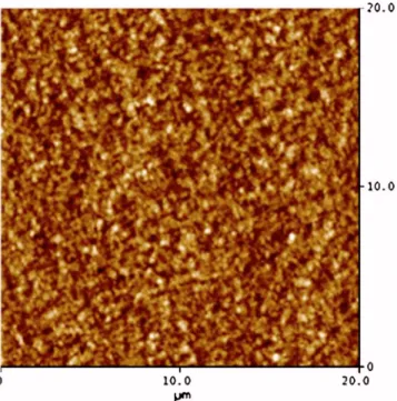
An atomic force microscopy image of the surface of the Ge film grown on the Si substrate with Si+ pre-ion-implantation is shown in Fig.4. The surface is smooth and no cross-hatch pattern is visible. For the current case, the disappearance of the cross-hatch pattern is because the meta-morphic buffer takes a three-dimensional growth mode in its initial stage, and the resulted behavior of the dislocations is different from that in the conventional composition graded GeSi layers.
In summary, a thin GexSi1−x metamorphic buffer layer for the growth of a high-quality Ge film on a Si substrate was achieved by using a Si+ on implantation on the Si substrate before the growth of the GexSi1−xmetamorphic buffer layers. The enhanced level of relaxation can be attributed to the introduction of point defects in the Si substrate with a heavy dose Si+implantation. Due to the use of the pre-ion-implantation technique and the interface blocking of the dis-locations in the GexSi1−x metamorphic buffer structure, the total thickness of the GexSi1−xmetamorphic buffer layer was greatly reduced to a thickness of 0.45m, which is much thinner than in the previous report.3Because the formation of the dislocation pileups in the GexSi1−x metamorphic buffer layer was eliminated, the surface of the Ge film grown was very smooth, no cross-hatch pattern could be observed and the dislocations in the top Ge layer were reduced to about 7.6⫻106cm−2. The approach described in this letter can be used to grow high-quality Ge film on a Si substrate and can also be easily applied to the fabrication of the Ge metal oxide
semiconductor field effect transistors and optoelectronic de-vices on Si substrates.
The authors would like to acknowledge the assistance and support of the National Science Council, Taiwan, R.O.C., under the Contract Nos. NSC 95-2752-E-009-001-PAE and 94-EC-17-A-05-S1-020. The authors also would like to thank Yu-Chun Lin and Shyh-Horng Hsiao of the Center for Nano Science and Technology for the X-ray dif-fraction measurements difdif-fraction measurements.
1H. Shang, K. L. Lee, P. Kozlowski, C. D’Emic, I. Babich, E. Sikorski, M.
Ieong, H. S. P. Wong, K. Guarini, and W. Haensch, IEEE Electron Device Lett. 25, 135共2004兲.
2J. Oh, S. K. Banerjee, and J. C. Campbell, IEEE Photonics Technol. Lett.
16, 581共2004兲.
3S. B. Samavedam and E. A. Fitzgerald, J. Appl. Phys. 81, 3108共1997兲. 4Y. Fukuda, Y. Kadota, and Y. Ohmachi, Jpn. J. Appl. Phys., Part 1 27, 485
共1988兲.
5R. D. Dupuis, J. C. Bean, J. M. Brown, A. T. Macrander, R. C. Miller, and
L. C. Hopkins, J. Electron. Mater. 16, 69共1987兲.
6S. Y. Shiryaev, F. Jensen, and J. W. Petersen, Appl. Phys. Lett. 64, 3305
共1994兲.
7V. S. Avrutin, N. F. Izyumskaya, A. F. Vyatkin, V. I. Zinenko, Yu. A.
Agafonov, D. V. Roshchupkin, E. A. Steinman, V. I. Vdovin, and T. G. Yugova, Mater. Sci. Eng., B 100, 35共2003兲.
8Kentarou Sawano, Yoshihisa Hirose, Yusuke Ozawa, Shinji Koh, Junji
Yamanaka, Kiyokazu Nakagawa, Takeo Hattori, and Yasuhiro Shiraki, Jpn. J. Appl. Phys., Part 1 42, 735共2003兲.
9Guangli Luo, Tsung-His Yang, Edward Yi Chang, Chun-Yen Chang, and
Koung-An Chao, Jpn. J. Appl. Phys., Part 1 42, 517共2003兲.
10J. W. Matthews and A. E. Blakeslee, J. Cryst. Growth 27, 118共1974兲. 11R. Hull and J. C. Bean, Appl. Phys. Lett. 54, 925共1989兲.
12Erich Kasper, Klara Lyutovich, Matthias Bauer, and Michael Oehme, Thin
Solid Films 336, 319共1998兲.
FIG. 4.共Color online兲 Atomic force microscopy image of the surface mor-phology of the sample with a Si+ pre-ion-implantation. The root mean
square共rms兲 of the roughness is 0.38 nm.
083507-3 Hsieh et al. Appl. Phys. Lett. 90, 083507共2007兲
This article is copyrighted as indicated in the article. Reuse of AIP content is subject to the terms at: http://scitation.aip.org/termsconditions. Downloaded to IP: 140.113.38.11 On: Thu, 01 May 2014 00:38:59