低功耗可重組固定寬度乘法器之設計與實作
72
0
0
全文
(2) 低功耗可重組固定寬度乘法器之設計與實作 Design and Implementation of Power-Efficient Reconfigurable Fixed-Width Multipliers 研 究 生:涂晉豪. Student:Jin-Hao Tu. 指導教授:范倫達博士. Advisor:Dr. Lan-Da Van. 國 立 交 通 大 學 資訊科學與工程研究所 碩 士 論 文. A Thesis Submitted to Institute of Computer Science and Engineering College of Computer Science National Chiao Tung University in partial Fulfillment of the Requirements for the Degree of Master in Computer Science July 2008 Hsinchu, Taiwan, Republic of China. 中華民國 九 十 七 年 七 月.
(3) 摘要. 低功耗可重組固定寬度乘法器之設計與實作. 學生:涂晉豪. 指導教授:范倫達 博士. 國立交通大學 資訊科學與工程研究所. 摘. 要. 在本論文中,我們提出了具有四種運算模式的可重組固定寬度 Booth 乘法器 以及可重組固定寬度 Baugh-Wooley 乘法器。此四種運算模式提供了高精準度運 算、平行運算、全精準度運算等特性,可因應多種不同的運算需求。根據模擬結 果,對於一個 16x16 可重組固定寬度 Booth 乘法器,平均四種運算模式的功率消 耗可比 16x16 非重組固定寬度 Booth 乘法器節省 14.0%的功率消耗。而 16x16 可重 組固定寬度 Baugh-Wooley 乘法器亦可節省 12.56%的功率消耗。另外我們將可重組 固定寬度乘法器應用於 FIR 濾波器中,藉此說明可重組固定寬度乘法器具有功率 調節的能力,進而達到省電的目的。. I.
(4) Abstract. Design and Implementation of Power-Efficient Reconfigurable Fixed-Width Multipliers. Student:Jin-Hao Tu. Advisor:Dr. Lan-Da Van. Institute of Computer Science and Engineering College of Computer Science National Chiao Tung University. ABSTRACT In this thesis, we propose a reconfigurable fixed-width Booth multiplier and a reconfigurable fixed-width Baugh-Wooley multiplier design framework that provides four configuration modes (CMs). The presented four configuration modes of the reconfigurable fixed-width multiplier are capable of providing high resolution, parallel, and full-precision multiplications for different computation demands. From the simulation results, the proposed 16x16 reconfigurable fixed-width Booth multiplier can attain the power saving of 14.0% on average with respect to that of the 16x16 non-reconfigurable fixed-width Booth multiplier. On the other hand, the proposed 16x16 reconfigurable fixed-width Baugh-Wooley multiplier can save 12.56% power consumption on average in comparison with that of the 16x16 non-reconfigurable fixed-width. Baugh-Wooley multiplier.. Furthermore,. we. apply the. proposed. reconfigurable multiplier to FIR filter to show the power scalable capability under four different modes.. II.
(5) 誌謝. 誌. 謝. 首先感謝指導教授 范倫達老師在這兩年多以來的悉心指導與建議,並提供我 各方面的協助,使我可以確立並完成我的論文研究。此外,亦要感謝王旭昇學長 無私地提供協助,讓我的研究得以順利地進行下去。其次是感謝 VIPLab 實驗室的 夥伴們,感謝你們在我的研究生生活中所帶來的溫馨與歡笑。 最後要感謝家人和親友們的關心、支持與鼓勵,尤其是親愛的爸爸媽媽,你 們讓我可以無後顧之憂的完成學業。再次感謝以上所有幫助過我的人,謹以此文 獻給你們。. III.
(6) Contents. Contents 摘. 要 ................................................................................................................. Ⅰ. ABSTRACT ........................................................................................................... Ⅱ 誌. 謝 ................................................................................................................. III. CONTENTS ........................................................................................................... Ⅳ LIST OF TABLES ................................................................................................. Ⅵ LIST OF FIGURES .............................................................................................. Ⅷ. Chapter 1. Introduction ......................................................................................... 1. 1.1 Motivation ..................................................................................................... 2 1.2 Thesis Organization....................................................................................... 3. Chapter 2. Fundemental Concepts ....................................................................... 4. 2.1 Array Multipliers ........................................................................................... 4 2.1.1 Booth Multiplier ................................................................................... 4 2.1.2 Baugh-Wooley Multliplier ................................................................... 7 2.2 Subword Multiplication ................................................................................ 8 2.3 Low-Error Fixed-Width Multipliers............................................................ 10. IV.
(7) Contents. Chapter 3. Design of Reconfigurable Fixed-width Multipliers ......................... 13. 3.1 Reconfigurable Fixed-Width Booth Multiplier ........................................... 13 3.1.1 CM1: nxn Fixed-Width Multiplier ..................................................... 14 3.1.2 CM2: Two n/2xn/2 Fixed-Width Multipliers ..................................... 16 3.1.3 CM3: n/2xn/2 Full-Precision Multiplier ............................................ 19 3.1.4 CM4: Sum of Two n/2xn/2 Fixed-Width Multipliers ........................ 22 3.1.5 Proposed Structure ............................................................................. 22 3.2 Reconfigurable Fixed-Width Baugh-Wooley Multiplier ............................ 26 3.2.1 CM1: nxn Fixed-Width Multiplier ..................................................... 28 3.2.2 CM2: Two n/2xn/2 Fixed-Width Multipliers ..................................... 30 3.2.3 CM3: n/2xn/2 Full-Precision Multiplier ............................................ 31 3.2.4 CM4: Two n/4xn/4 Full-Precision Multipliers ................................... 32 3.2.5 Proposed Structure ............................................................................. 34. Chapter 4. Implenmentation and Comparison ................................................... 44. 4.1 Simulation Results of Reconfigurable Fixed-Width Multiplier .................. 45 4.1.1 Reconfigurable Fixed-Width Booth Multiplier .................................. 46 4.1.2 Reconfigurable Fixed-Width Baugh-Wooley Multiplier ................... 48 4.2 Application of Reconfigurable Fixed-Width Multiplier.............................. 52. Chapter 5. Conclusion and Future Work ........................................................... 55. Bibliography .......................................................................................................... 56. Biography ............................................................................................................... 60. V.
(8) List of Tables. List of Tables Chapter 2 2.1:. Modified Booth recoding table ....................................................................... 6. Chapter 3 3.1:. Proposed four configuration modes of the reconfigurable fixed-width Booth multiplier ....................................................................................................... 14. 3.2:. Truth table of the decoder for the reconfigurable fixed-width Booth multiplier ....................................................................................................... 26. 3.3:. Truth table of sub-calibration-circuit1 (SCC1) and sub-calibration-circuit2 (SCC2) .......................................................................................................... 26. 3.4:. Proposed four configuration modes of the reconfigurable fixed-width Baugh-Wooley multiplier .............................................................................. 28. 3.5:. Truth table of the decoder for the reconfigurable fixed-width Baugh-Wooley multiplier ....................................................................................................... 36. Chapter 4 4.1:. Qualitative comparison between different reconfigurable architectures ...... 45. 4.2:. Chip Characteristics of the 8x8 reconfigurable fixed-width Booth multipliers and the 8x8 non-reconfigurable fixed-width Booth multipliers.................... 47. VI.
(9) List of tables. 4.3:. Chip Characteristics of the 16x16 reconfigurable fixed-width Booth multipliers and the 16x16 non-reconfigurable fixed-width Booth multipliers ....................................................................................................................... 48. 4.4:. Chip Characteristics of the 8x8 reconfigurable fixed-width Baugh-Wooley multipliers and the 8x8 non-reconfigurable fixed-width Baugh-Wooley multipliers ..................................................................................................... 50. 4.5:. Chip Characteristics of the 16x16 reconfigurable fixed-width Baugh-Wooley multipliers and the 16x16 non-reconfigurable fixed-width Baugh-Wooley multipliers ..................................................................................................... 50. 4.6:. Chip Characteristics of the 24x24 reconfigurable fixed-width Baugh-Wooley multipliers and the 24x24 non-reconfigurable fixed-width Baugh-Wooley multipliers ..................................................................................................... 51. 4.7:. Chip Characteristics of the 32x32 reconfigurable fixed-width Baugh-Wooley multipliers and the 32x32 non-reconfigurable fixed-width Baugh-Wooley multipliers ..................................................................................................... 51. 4.8:. Comparison results of error signals and power consumption obtained with the proposed 8x8 reconfigurable fixed-width Booth multiplier for FIR filter application ..................................................................................................... 54. 4.9:. Comparison results among FIR filters .......................................................... 54. VII.
(10) List of Figures. List of Figures Chapter 2 2.1:. Block diagram of Booth recoding circuit ........................................................ 6. 2.2:. Modified Booth partial-product diagram with sign-generate sign extension scheme for an nxn multiplier........................................................................... 7. 2.3:. Partial-product array diagram for an nxn Baugh-Wooley multiplier .............. 8. 2.4:. Subword multiplication (a) two n/2xn/2 multiplications, (b) two n/2xn/2 partial-product array distribution, (c) four n/4xn/4 multiplications, and (d) four n/4xn/4 partial-product array distribution ............................................... 9. 2.5:. The fixed-width 8 8 Booth multiplier with Q0,w1 .........................................11. 2.6:. (a) The fixed-width 8 8 Baugh-Wooley multiplier with Q 0,w1 , and (b) logic diagrams of AOR, ANOR, AHA, AFA, NFA ....................................... 12. Chapter 3 3.1:. Prototype structure of the proposed reconfigurable fixed-width Booth multiplier involving MUL1, MUL2, and discarding truncated region of LSP ....................................................................................................................... 14. 3.2:. (a) Partial-product array diagram for nxn fixed-width multiplier with n=8, and (b) configuration parameter settings....................................................... 15. VIII.
(11) List of figures. 3.3:. Subword operation for two n/2xn/2 fixed-width multiplications ................. 17. 3.4:. (a) Partial-product array diagram for two n/2xn/2 fixed-width multipliers with n=8, (b) configuration settings of S2,4 and S3,4, (c) configuration parameter settings, and (d) configured Booth recoding circuit ..................... 18. 3.5:. Subword operation for one n/2xn/2 full-precision multiplication ................ 20. 3.6:. (a) Partial-product array diagram for n/2xn/2 full-precision multiplier with n=8, (b) configuration settings of S2,4 and S3,4, (c) configuration parameter settings, and (d) configured Booth recoding circuit ...................................... 21. 3.7:. Partial-product array diagram for sum of two n/2xn/2 fixed-width multipliers with n=8 ........................................................................................................ 22. 3.8:. Overall structure of the proposed reconfigured fixed-width Booth multiplier for n=8 ........................................................................................................... 25. 3.9: 3.10:. Logical diagram of SCC1 and SCC2 ............................................................ 26 Prototype structure of the proposed reconfigurable fixed-width Baugh-Wooley multiplier involving MUL1, MUL2, MUL3 and discarding truncated region of LSP .............................................................................. 27. 3.11:. (a) Partial-product array diagram for nxn fixed-width multiplication, (b) proposed partial-product array diagram using MUL1, MUL2, and MUL3 for CM1, and (c) configuration parameter settings ..................................... 29. 3.12:. Subword operation for two n/2xn/2 fixed-width multiplications ............... 31. 3.13:. (a) Proposed partial-product array diagram for CM2, and (b) configuration parameter settings........................................................................................ 31. 3.14:. (a) Proposed partial-product array diagram for CM3, and (b) configuration. IX.
(12) List of figures. parameter settings........................................................................................ 32 3.15:. Subword operation for two n/4xn/4 full-precision multiplications............. 33. 3.16:. (a) Proposed partial-product array diagram for CM4, and (b) configuration parameter settings........................................................................................ 33. 3.17:. Proposed pipelined reconfigurable multiplier ............................................. 36. 3.18:. Structure of MUL1 ...................................................................................... 37. 3.19:. Structure of MUL2 ...................................................................................... 37. 3.20:. Structure of MUL3 ...................................................................................... 38. 3.21:. Logic diagrams of the other processing elements ....................................... 39. 3.22:. Proposed power-efficient pipelined reconfigurable fixed-width Baugh-Wooley multiplier ............................................................................ 42. Chapter 4 4.1:. Proposed reconfigurable fixed-width Booth multiplier layout for n=8 ........ 47. 4.2:. Proposed pipelined reconfigurable fixed-width Baugh-Wooley multiplier layout for n=16 .............................................................................................. 49. X.
(13) Chapter 1. Introduction. Chapter 1 Introduction During the past decade, the multipliers [1-32] in VLSI signal processing systems stand the test for multimedia-communication applications. Among these multipliers, the basic multiplication either follows Booth [1-3] or Baugh-Wooley algorithms [4]. In many digital signal processing (DSP) algorithms such as digital filters, discrete cosine transform (DCT), and wavelet transform, it is desirable to provide full-precision multiplication [5-8], and fixed-width multiplication [9-20] that produces n-bit output product with n-bit multiplier and n-bit multiplicand with low truncation error. A fixed-width multiplier (also referred to as single precision multiplier) with area and power saving can be achieved either by directly truncating n least significant columns and preserving n most significant columns or by other efficient methods [9-20]. By the former method, significant truncation errors will be introduced since no error compensation is considered. Thus, the latter schemes explore issues on low truncation error and small area. Lim [9] first utilized statistical techniques to estimate and simulate the error-compensation bias. However, in his analysis, the reduction and rounding errors are separately treated such that this scheme does not lead to an accurate enough error-compensation bias. Note that the sum of the reduction and rounding errors equals the. truncation. error. [10].. In. [10-11],. the. presented. work. improved. the. error-compensation bias to be more accurate and practical since the reduction and rounding errors are concurrently treated. Later, in [12-20], many researchers analyzed 1.
(14) Chapter 1. Introduction. an adaptive error-compensation bias under keeping n w most significant columns and proposed various fixed-width multipliers. On the other hand, much work, recently, focuses on constructing reconfigurable full-precision multipliers [21-31]. In [21-26], one reconfigurable full-precision multiplier has been proposed by the subword partitioning technique, where one nxn, two n/2xn/2, or four n/4xn/4 full-precision multiplications can be performed. In [27-29], a reconfigurable full-precision multiplier consists of an array of 4x4 or 8x8 small multipliers, where the multiplier introduced in [28] has more configuration modes than that of [27, 29]. The complicated reconfigurable architecture can provide multiple 4x4, 8x8, 16x16, 32x32, and 64x64 operations and support unsigned, signed and 2’s-complement multiplications. Nevertheless, the architecture [28] led to larger hardware area. The low-power multiplier designs are debated in [30-32]. In [30], a 2-D pipeline gating technique is employed to design a power-aware array multiplier that is adaptive to the high or low resolution operations. In [31], the power cut-off technique is employed to reduce power consumption when lower resolution multiplication is demanded. In [32], a Baugh-Wooley multiplier made use of the dynamic range detection unit and truncated multiplication technique to save power consumption. Nevertheless, the proposed multiplier provided only truncated output precisions under nxn truncated multiplication and didn’t discuss how to generate the full-precision multipliers and other fixed-width type multiplier.. 1.1 Motivation As growing demands on portable computing and communication systems, the power-efficient multiplier plays an important role in very large-scale integration (VLSI) systems. As we know that the conventional reconfigurable multiplier designs [21-31] are based on the full-precision multiplier infrastructure to generate the full-precision multipliers. However, it can be seen that the full-precision multiplier is much more cost ineffective and 2.
(15) Chapter 1. Introduction. power-inefficient than the fixed-width multipliers [19-20]. The fixed-width multiplier and the reconfigurable multiplier are two feasible approaches for the design of power-efficient multipliers. To our best knowledge, we are the first one to explore the power-efficient reconfigurable fixed-width multiplier and discuss how to reconfigure the structure to generate a family of useful fixed-width and full-precision multipliers.. 1.2 Thesis Organization The rest of the paper is organized as follows. The Booth multiplier, Baugh-Wooley multiplier, subword multiplication and low-error fixed-width multiplier are briefly reviewed in Chapter 2. In Chapter 3, the proposed reconfigurable fixed-width multiplication engine with four configuration modes is presented. The comparison results in terms of area size and power saving are presented in Chapter 4. For FIR filter application, the error comparison and power scalable performance using various fixed-width and full-precision multipliers are illustrated in the same chapter. Last, brief statements conclude the presentation of this thesis.. 3.
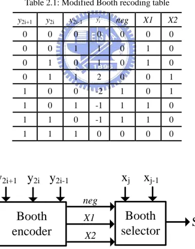
(16) Chapter 2. Fundamental Concepts. Chapter 2 Fundamental Concepts In this chapter, the fundamental concepts will be given, including the introduction to the Booth multiplier, Baugh-Wooley multiplier, subword multiplication, and low-error fixed-width multiplier.. 2.1 Array Multipliers In this thesis, we will introduce two kinds of reconfigurable fixed-width multipliers. One is based on the Booth multiplier and the other is based on the Baugh-Wooley multiplier. The Booth and Baugh-Wooley multipliers are very famous algorithms used in digital signal processing. In the following, we will briefly review these two algorithms.. 2.1.1 Booth Multiplier Considering two 2’s-complement integer operands, we can respectively represent an n-bit multiplicand X and an n-bit multiplier Y as follows. n-2. x 2. X = -xn-1 2 n 1 +. i. i. (1). i=0. Y = -yn-1 2 n 1 +. n-2. y 2 i=0. 4. i. i. (2).
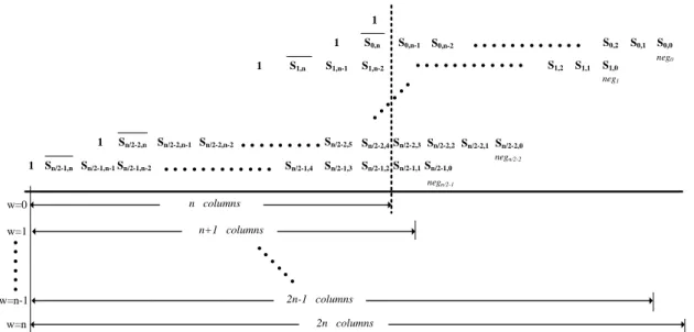
(17) Chapter 2. Fundamental Concepts. where x i , y i {0, 1} . The 2n -bit full-precision product PFP can be written as PFP X Y. (3). If n is even, Y can be rewritten as ( n-2) / 2. y 2. Y=. 2i. i. (4). i=0. where yi = y2i 1 y2i 2 y2i 1 and y 1 0 .The term yi has a value of {-2, -1, 0, 1, 2}. Each recoded value performs a certain operation on the multiplicand X ; the multiple additions at each stage are required to generate the product. Substituting (4) into (3), we obtain ( n 2) / 2. PFP =. . ( n 2) / 2. yi X 22i . S. i. i 0. i=0. (5). where Si =yi X 22i . Triplet scanning takes place from y-1 to the most significant bit (MSB) with a one-bit overlap. Table 2.1 lists the recoding rule and Fig. 2.1 shows the block diagram of the Booth recoding circuit. In Fig. 2.1, the Booth encoder generates three Booth recoding bits neg, X1, and X2 to the Booth selector and then the Booth selector selects input multiplicand {xj, xj-1} as output partial products. In order to simplify the representation of each partial product, we define the following notation. Si Si,n1 2 2i n1 Si,n2 2 2i n2 Si ,n3 2 2i n3 ... Si ,0 2 2i. where. Si , j. (6). represents the j-th bit product of the i-th row. In conventional. 2’s-complement Booth arithmetic operations, the partial product sign extensions are required for each stage, but these extended sign bits lead to large amount of area and power overhead. The sign S of an n by n multiplier can be expressed as 2 n 1. S =( S 0, n. . 2n 3. 2 j )20 ( S1, n. j n. j n. n 1. ( S n / 2 1, n. . 2 j ) 2 2 ( S 2, n. 2 )2 j. 2( n / 2 1). j n. 5. 2n 5. 2 )2 j. j n. 4.
(18) Chapter 2. Fundamental Concepts. =(2n 1 S0, n 2n ) (2n 3 S1, n 2n 2 ) (2n 5 S2, n 2n 4 ) (22n 1 Sn / 2 1, n 22n 2 ) 2n. (7). Substituting (6) and (7) into (5), we can obtain the partial-product array diagram for nxn Booth multiplier as depicted in Fig. 2.2, where notation w means to keep n+w most significant columns of the partial products for fixed-width multiplications. If w=n, the fixed-width multiplier becomes a full-precision multiplier. In this thesis, we would like to reconfigure the fixed-width multiplication engine to generate several useful multipliers under the limited hardware resource for DSP and image processing applications.. Table 2.1: Modified Booth recoding table y2i+1. y2i. y2i-1. yi. neg. X1. X2. 0. 0. 0. 0. 0. 0. 0. 0. 0. 1. 1. 0. 1. 0. 0. 1. 0. 1. 0. 1. 0. 0. 1. 1. 2. 0. 0. 1. 1. 0. 0. -2. 1. 0. 1. 1. 0. 1. -1. 1. 1. 0. 1. 1. 0. -1. 1. 1. 0. 1. 1. 1. 0. 0. 0. 0. xj. xj-1. y2i+1 y2i y2i-1 neg. Booth encoder. X1 X2. Booth selector. Fig. 2.1. Block diagram of Booth recoding circuit.. 6. Si.
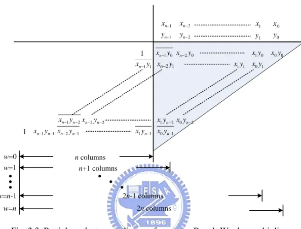
(19) Chapter 2. Fundamental Concepts. 1. S1,n. 1. 1. S0,n. S1,n-1. S1,n-2. ………… ………… S S. S0,n-1. S0,n-2. 1,2. 1,1. S0,2 S1,0. S0,1 S0,0 neg0. …. neg1. …. 1. 1 Sn/2-1,n Sn/2-1,n-1 Sn/2-1,n-2. w=0 w=1. ……… S ………… S S. Sn/2-2,n Sn/2-2,n-1 Sn/2-2,n-2. n/2-1,4. n/2-2,5. Sn/2-2,4 Sn/2-2,3 Sn/2-2,2 Sn/2-2,1 Sn/2-2,0. n/2-1,3. Sn/2-1,2 Sn/2-1,1 Sn/2-1,0. negn/2-2. negn/2-1. n columns n+1 columns. …. ……. … 2n-1 columns. w=n-1. 2n columns. w=n. Fig. 2.2. Modified Booth partial-product diagram with sign-generate sign extension scheme for an nxn multiplier.. 2.1.2 Baugh-Wooley Multiplier Considering two 2’s-complement integer operands, we can respectively represent an n-bit multiplicand X and an n-bit multiplier Y as (1) and (2). The 2n-bit full-precision product PFP can be written as PFP X Y n-2 n-2. x y 2. xn-1 yn-1 2 2n-2 +. i. i+j. j. i=0 j=0. n-2. x. +2 n-1 (-2 n-1+. n-1 y j 2. j. + 1). j=0 n-2. y. 2n-1 (-2n-1+. i=0. i n-1 xi 2 + 1). (8). Eq. (8) represents the Baugh-Wooley algorithm [4-6] in which this array multiplier sums partial-product bits corresponding to each weighting. The partial-product array for nxn 2’s-complement multiplication are depicted in Fig. 2.3, where notation w means to keep n+w most significant columns of the partial products for fixed-width multiplications. If w=n, the fixed-width multiplier becomes a full-precision multiplier. 7.
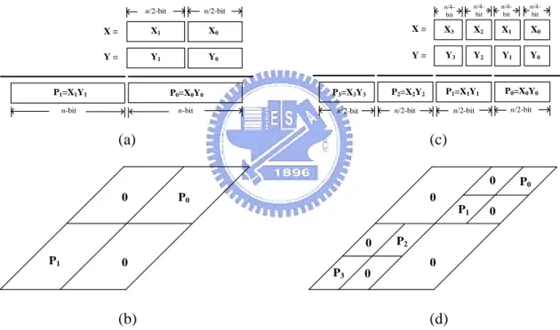
(20) Chapter 2. Fundamental Concepts. In this thesis, we would like to reconfigure the fixed-width multiplication engine to generate four useful multipliers under the limited hardware resource.. xn 1 yn1. xn 2. x1. yn 2. y1. xn1 y0 xn 2 y0 xn1 y1 xn2 y1 1. xn 1 yn 2 xn 2 yn 2. n columns n+1 columns . x1 y0 x0 y0 x0 y1. x1 yn 2 x0 yn 2. 1 xn 1 yn 1 xn 2 yn 1 w=0 w=1 w=n-1. x1 y1. x0 y0. x1 yn 1 x0 yn 1. 2n-1 columns. w=n. 2n columns. Fig. 2.3. Partial-product array diagram for an nxn Baugh-Wooley multiplier.. 2.2 Subword Multiplication Many DSP and computer applications demand to operate at lower resolution, where the data can be expressed in a half-word length [21-26]. Generally, applying the subword multiplication scheme, we can partition an n-bit operand into two independent n/2-bit operands or four independent n/4-bit operands; hence, the subword multiplier can perform not only nxn full-precision multiplication but also two n/2xn/2 or four n/4xn/4 full-precision multiplications in parallel. Fig. 2.4 illustrates subword multiplication and the partial product array distribution [21-26]. In Fig. 2.4(a), two n-bit operands, X and Y, are partitioned into two independent pairs of n/2-bit subwords, and. 8.
(21) Chapter 2. Fundamental Concepts. then the two pairs of n/2-bit subwords are multiplied to produce two independent n-bit products: P1=X1Y1 and P0=X0Y0, where the partial product array distribution is addressed in Fig. 2.4(b). On the other hand, n/4xn/4 subword multiplication and the partial product array distribution are illustrated in Fig. 2.4(c) and 2.4(d), respectively. To our best knowledge, the current subword scheme is applied only to full-precision multiplication based on the full-precision multiplier infrastructure. In the following section, we will extend this subword scheme to fixed-width and full-precision multiplication using the fixed-width prototype multiplier.. n/2-bit. n/2-bit. X=. X1. X0. Y=. Y1. Y0. P1=X1Y1. P0=X0Y0. P3=X3Y3. n-bit. n-bit. n/2-bit. n/4bit. n/4bit. n/4bit. n/4bit. X=. X3. X2. X1. X0. Y=. Y3. Y2. Y1. Y0. P2=X2Y2. P1=X1Y1. P0=X0Y0. n/2-bit. n/2-bit. n/2-bit. (a). (c) 0. 0. P0. P1 0. P1. P0. 0. 0. P3. (b). 0. P2 0. 0. (d). Fig. 2.4. Subword multiplication (a) two n/2xn/2 multiplications, (b) two n/2xn/2 partial-product array distribution, (c) four n/4xn/4 multiplications, and (d) four n/4xn/4 partial-product array distribution.. 2.3 Low-Error Fixed-Width Multipliers It is known that the various fixed-width multipliers with adaptive compensation biases have been widely discussed in [12-20]. Herein, regarding the tradeoffs of the 9.
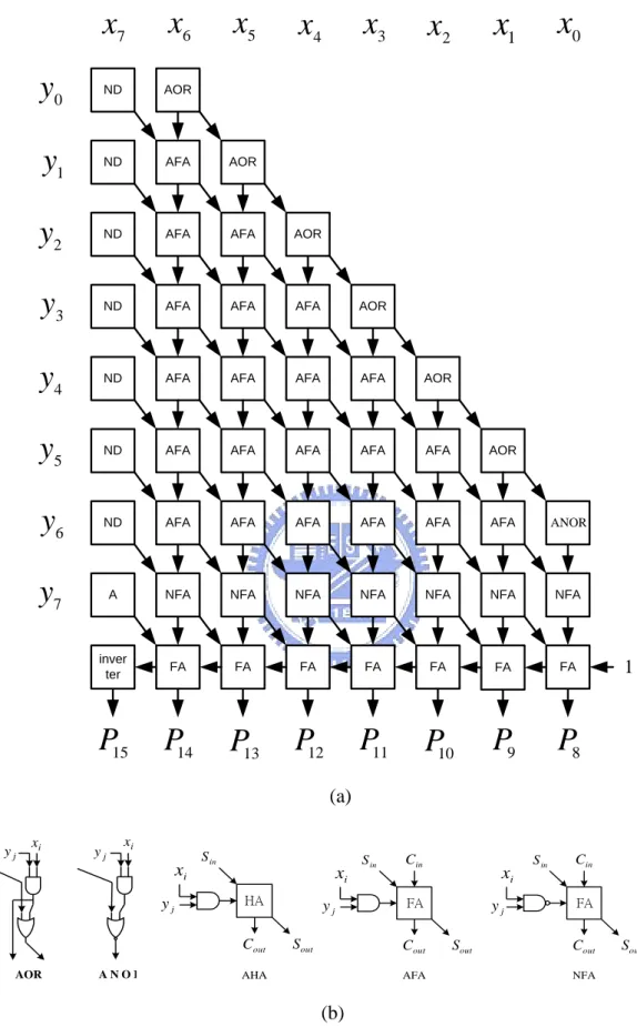
(22) Chapter 2. Fundamental Concepts. truncation error and area cost in [19-20], we choose w=1 (i.e., keeping n+1 most significant columns) and Q=0 for the prototype multiplier structure, where Q has been clearly defined in [19-20]. The error-compensation bias can be summarized as. Type1,Q 0, w1 1 1 ( E main Q 0 ,w1 ) , if Q 0 ,w1 0 2 2 1 ( E main Q 0 ,w1 ) 0 , if Q 0 ,w1 0 2 . (9). where Emain =S0,n-1+S1,n-3+S2,n-5+ · · ·+Sn/2-2,3+Sn/2-1,1 (i.e., the (n+1)th column counted from left to right of Fig. 2.2) and Q 0,w1 = S0,n-2 +S1,n-4+S2,n-6+ · · ·+Sn/2-2,2+Sn/2-1,0 (i.e., the (n+2)th column counted from left to right of Fig. 2.2) for the Booth architecture. If the Baugh-Wooley architecture is the basic multiplier, Emain = xn1 y0 + xn-2y1+ xn-3y2 + · · ·+ x1yn-2+ x0 yn1 (i.e., the (n+1)th column counted from left to right of Fig. 2.3) and Q 0 ,w1 = xn-2y0 + xn-3y1+ xn-4y2+ · · ·+ x1yn-3+ x0yn-2 (i.e., the (n+2)th column counted. from left to right of Fig. 2.3). Fig. 2.5 and Fig. 2.6(a) are the prototype Booth multiplier structure and the prototype Baugh-Wooley multiplier structure for n=8, respectively, where A, ND, HA, and FA denote AND gate, NAND gate, a half adder and a full adder, respectively, and the logic diagrams of the other processing elements are depicted in Fig. 2.6(b).. 10.
(23) Chapter 2. Fundamental Concepts x7. Y[1:0],0. x6. x5. Ctrl0[2:0]. Booth encoder. sel x7. Y[3:1]. x6. sel. x5. x4. sel x3. Ctrl1[2:0] Booth encoder. sel. sel. sel. sel. 1 HA. x7. Y[5:3]. x6. x5. x4. sel. 1 FA. FA. x3. x2. x1. Ctrl2[2:0] Booth encoder. sel. sel. sel. sel. sel. sel. sel. 1 HA Ctrl3[2:0] Y[7:5] Booth encoder. x7. sel. x6. x5. sel. sel. x4. sel. FA. FA. FA. FA. x3. x2. x1. x0. sel. sel. sel. sel. sel. 1 HA. FA. FA. FA. FA. FA. FA. FA. 1. HA. FA. FA. FA. FA. FA. FA. FA. P15. P14. P13. P12. P11. P10. P9. P8. Fig. 2.5. The fixed-width 8 8 Booth multiplier with. 11. Q 0,w1. 0. ..
(24) Chapter 2. x5. Fundamental Concepts. x0. x7. x6. y0. ND. AOR. y1. ND. AFA. AOR. y2. ND. AFA. AFA. AOR. y3. ND. AFA. AFA. AFA. AOR. y4. ND. AFA. AFA. AFA. AFA. AOR. y5. ND. AFA. AFA. AFA. AFA. AFA. AOR. y6. ND. AFA. AFA. AFA. AFA. AFA. AFA. ANOR. y7. A. NFA. NFA. NFA. NFA. NFA. NFA. NFA. inver ter. FA. FA. FA. FA. FA. FA. FA. P15. P14. P13. P12. P11. P10. P9. P8. x3. x4. x1. x2. 1. (a) yj. xi. yj. xi. xi yj. S in. xi HA. Cout AOR. ANOR. S in. yj Sout. Cin FA. Cout. AHA. xi. AFA. yj Sout. S in. Cin FA. Cout. Sout. NFA. (b) Fig. 2.6. (a) The fixed-width 8 8 Baugh-Wooley multiplier with Q 0,w1 , and (b) logic diagrams of AOR, ANOR, AHA, AFA, NFA.. 12.
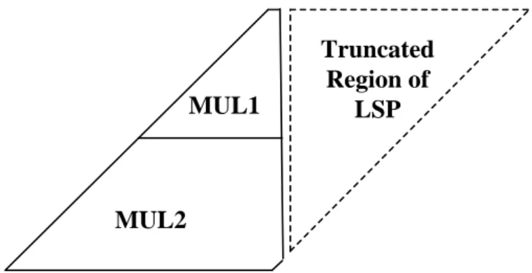
(25) Chapter 3. Design of Reconfigurable Fixed-Width Multipliers. Chapter 3 Design of Reconfigurable Fixed-Width Multipliers In this chapter, we describe the design methodology of the reconfigurable fixed-width multipliers based on the Booth architecture and the Baugh-Wooley architecture, respectively.. 3.1 Reconfigurable Fixed-Width Booth Multiplier In this section, we begin to demonstrate how to generate four different multipliers under the limited hardware resource of the fixed-width Booth multiplier. In this thesis, we use the fixed-width multiplier in Fig. 3.1 as our reconfigurable Booth multiplier prototype instead of the full-precision multiplier structure, where the fixed-width multiplier truncates partial products of the least significant part (LSP) as shown in the dash-lined region of Fig. 3.1 and compensate the error with adaptive compensation bias. In Fig. 3.1, two modules denoted as MUL1 and MUL2 are used to reconfigure the following four different multipliers as listed in Table 3.1 through the corresponding four configuration modes (CMs). Thus, the proposed reconfigurable fixed-width Booth multiplier employing MUL1 and MUL2 is essentially different from the full-precision one [21-31]. Without loss of the generality, we use n=8 to investigate each CM case.. 13.
(26) Chapter 3. Design of Reconfigurable Fixed-Width Multipliers. Truncated Region of LSP. MUL1. MUL2. Fig. 3.1. Prototype structure of the proposed reconfigurable fixed-width Booth multiplier involving MUL1, MUL2, and discarding truncated region of LSP.. Table 3.1: Proposed four configuration modes of the reconfigurable fixed-width Booth multiplier Configuration Mode (CM). Function Descriptions. Mode Applications. CM1. nxn fixed-width multiplier. High resolution computations: Multiplication, matrix multiplication, square-root operation, filter, transform. CM2. two n/2xn/2 fixed-width multipliers. Parallel computations: Multiplication, matrix multiplication, square-root operation, filter, transform. CM3. n/2xn/2 full-precision multiplier. Full-precision computations: Multiplication, matrix multiplication, square-root operation, filter, transform. CM4. sum of two n/2xn/2 fixed-width multipliers. Parallel multiplication and add computations: Matrix multiplication, filter, transform. 3.1.1 CM1: nxn Fixed-Width Multiplier CM1 is in charge of operating nxn fixed-width multiplication that receives two n-bit numbers and produces an n-bit product. Since CM1 is confined to w=1, the partial-product array diagram as shown in Fig. 3.2(a) with n=8 can be easily obtained from Fig. 2.2. The partial products in the dash-lined region of Fig. 3.2(a) denoted as σCM1 14.
(27) Chapter 3. Design of Reconfigurable Fixed-Width Multipliers. are used to compute the error compensation bias in (9). Note that the error performance results of the Booth-based CM1 are the same as those of [20] because we implement the same adaptive compensation bias circuits. Throughout the section 3.1, in order to completely achieve four configuration modes, we provide three configuration parameters CP0, CP1, and CP2 combining with the partial product setting to generate four multipliers. For the fixed-width multiplier with n=8, the bit position of these parameters are shown in Fig. 3.2(a). In CM1, CP0, CP1, and CP2 are set to 0 as shown in Fig. 3.2(b). Associated with CP0, CP1, and CP2, the product of CM1 can be generally expressed as PCM 1 {P2 n1 , P2 n2 , P2 n3 ,...,Pn } ( n 2 ) / 2 2i. . S i 0. (2. n1. i ,n j. 2 2i n j. j 1. S 0,n 2 n ) (2 n3 S1,n 2 n2 ). (2 n5 S 2,n 2 n4 ) (2 2 n1 S n / 21,n 2 2 n2 ) 2 n 3n. 3n. CM 1 CP0 2 n CP1 2 2 CP2 2 2 MUL1. 2. (10). 1. σCM1 1 S0,8 S0,7 S0,6 1 S1,8 S1,7 S1,6 S1,5 S1,4 MUL2. CP1. CP0. 1 S2,8 S2,7 S2,6 S2,5 S2,4 S2,3 S2,2. +). 1 S3,8 S3,7 S3,6 S3,5 S3,4 S3,3 S3,2 S3,1 S3,0 CP2 P15 P14 P13 P12 P11 P10 P9. P8. (a) CP0. CP1. CP2. configure to. 0. 0. 0. (b) Fig. 3.2. (a) Partial-product array diagram for nxn fixed-width multiplier with n=8, and (b) configuration parameter settings. 15.
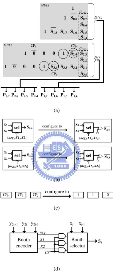
(28) Chapter 3. Design of Reconfigurable Fixed-Width Multipliers. 3.1.2 CM2: Two n/2xn/2 Fixed-Width Multipliers CM2 plays a role of concurrently performing two n/2xn/2 fixed-width multiplications. In this configuration mode, we need two copies of hardware resource to implement CM2. The corresponding fixed-width subword operation of CM2 is illustrated in Fig. 3.3, where two subword products are X1Y0 and X0Y1 because of the limited hardware resource and each fixed-width multiplication has n/2-bit wide output. Note that we can produce subword products X0Y0 and X1Y1 as the conventional subword multiplication by exchanging X0 and X1 before the Booth selector. However, X0Y0 and X1Y1 will lead to larger exchange hardware overhead. Thus, we adopt X1Y0 and X0Y1 subword operations. The partial-product array diagram is depicted in Fig. 3.4(a), where σCM2-1 and σCM2-2 denote the error compensation biases of X1Y0 and X0Y1, respectively. In Fig. 3.4(a) with n=8, compared with CM1, MUL1 can be unchanged while MUL2 must configure { S3,4 , S2,4 } to { S3,4 , S2,4 }, and { S3,5 , S2,5 } to { 1,1 } circled by dash-line and solid-line, respectively. In the logic gate level, we OR the original partial-product with the control signal to generate 1 and use XOR gate to produce inverted sign-bit as shown in Fig. 3.4(b), where CS denotes the control signal and note that the input {x4, x3} are configured to {x3, x3}. In addition, S2,6, S2,7, S3,6 ,and S3,7 are set to zero. The configuration parameter settings of CM2 are addressed in Fig. 3.4(c), where CP0, CP1, and CP2 are set to 1, 1, and 0, respectively. Since other partial products are configured to 0, we do not need to AND these partial products with control signal. Our approach is to AND three Booth recoding bits with the control signal as shown in Fig. 3.4(d) to save the number of AND gates while n increases. Hence, no matter how many partial products needed to be configured to 0, we merely require three AND gates if these partial products are in the same row. In addition, due to permanent inverted MSB output of the partial products in MUL2, the bits denoted as 0 represent one, but 16.
(29) Chapter 3. Design of Reconfigurable Fixed-Width Multipliers. the summation result of the most significant half of MUL2 still produces zero. In summary, the two products of CM2 can be generally expressed in (11a) and (11b). PCM 21 {P1,n1 , P1,n2 , P1,n3 ,...,P1,n / 2 } ( n / 2 2 ) / 2 2i. . S. (2. n / 21. i 0. i ,n j. 2 2i ( n / 2 ) j. j 1. S 0,n 2 n / 2 ) (2 n / 23 S1,n 2 n / 2 2 ). ( 2 n / 25 S 2 ,n 2 n / 2 4 ) (2 n1 S ( n / 22) / 2,n 2 n2 ) 2 n / 2 CM 21. (11a). PCM 22 {P2,n1 , P2,n2 , P2,n3 ,...,P2,n / 2 } ( n2) / 2. . . 2i. S. i ,n j i ( n / 22) / 21 j ( n / 2)1. 2 2i ( n / 2 ) j. (2 n / 21 S ( n / 22) / 21,n / 2 2 n / 2 ) ( 2 n / 2 3 S ( n / 2 2 ) / 2 2 , n / 2 2 n / 2 2 ) (2 n / 25 S ( n / 22) / 23,n / 2 2 n / 24 ) (2 n1 S ( n2) / 2,n / 2 2 n2 ) CM 22 CP0 2 n / 2 CP2 2 n2. where. (11b). { S( n / 22) / 21,n / 2 , S(n / 22) / 2 2,n / 2 , S(n / 22) / 23,n / 2 , , S( n2) / 2,n / 2 }. are the reconfigured. partial products as similar to that in Fig. 3.4(b), rather than to complement these partial-products of CM1.. n/2-bit. n/2-bit. X=. X1. X0. Y=. Y1. Y0. P1=X0Y1. P0=X1Y0. n/2-bit. n/2-bit. Fig. 3.3. Subword operation for two n/2xn/2 fixed-width multiplications.. 17.
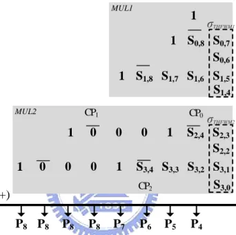
(30) Chapter 3. Design of Reconfigurable Fixed-Width Multipliers. MUL1. 1. σCM2-1 S0,7 S0,6. 1 S0,8. X1Y0. 1 S1,8 S1,7 S1,6 S1,5 S1,4 MUL2. CP1. 0. 1 0. 1. 0. 0. CP0. 0 1. 0. 1. S3,4 S3,3 CP2. σCM2-2 S2,4 S2,3 S2,2 S3,2 S3,1 S3,0. X0Y1. P2,7 P2,6 P2,5 P2,4 P1,7 P1,6 P1,5 P1,4. (a) x3. sel. x4. x3. configure to. S2,4. {neg2,X12,X22}. x3. sel. x4. sel. x3. S2,4 cs. {neg2,X12,X22}. x3. configure to. S3,4. sel. x3. S3,4 cs. {neg3,X13,X23}. {neg3,X13,X23}. (b) CP0. CP1. configure to. CP2. 1. 0. 1. (c) xj. y2i+1 y2i y2i-1. xj-1. neg. Booth encoder. Booth selector. X1 X2 CS. Si. (d) Fig. 3.4. (a) Partial-product array diagram for two n/2xn/2 fixed-width multipliers with n=8, (b) configuration settings of S2,4 and S3,4, (c) configuration parameter settings, and (d) configured Booth recoding circuit. 18.
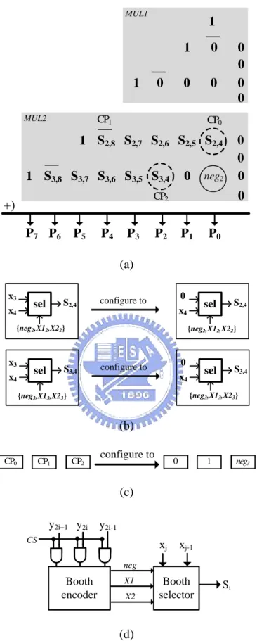
(31) Chapter 3. Design of Reconfigurable Fixed-Width Multipliers. 3.1.3 CM3: n/2xn/2 Full-Precision Multiplier CM3 serves as performing an n/2xn/2 full-precision multiplication. The corresponding subword operation of CM3 is illustrated in Fig. 3.5, where the subword product is X1Y1 with n-bit wide output. Since the proposed reconfigurable structure to implement full-precision multiplication is based on the fixed-width multiplier fabric, it can be seen that MUL2 is able to achieve this mode operation. Next, the partial-product array diagram is depicted in Fig. 3.6(a) with n=8, where the configuration of S2,4 and S3,4 circled by dash-line are different from the ones of other modes because their multiplicand inputs of the Booth selector have to be configured from {x4, x3} to {x4, 0} as shown in Fig. 3.6(b). The partial-product S3,2 is configured to neg2 circled by solid-line for 2’s-complement computation. In addition, S2,2, S2,3, S3,0, S3,1, and S3,3 are configured to 0 in MUL2. In this mode, the output of MUL1 needs to generate zero as shown in the upper diagram of Fig. 3.6(a). The configuration parameter settings of CM3 are addressed in Fig. 3.6(c), where CP0, CP1, and CP2 are set to 0, 1, and negn/2-1, respectively. For n=8, negn/2-1 is neg3. On the other hand, we AND three Booth recoding bits with the control signals to generate 0 in MUL2 as mentioned in the above paragraph. However, in order to generate 0 in MUL1, we can use AND gates before the Booth encoder to AND the multiplier inputs with the control signal as shown in Fig. 3.6(d) such that the Booth encoder generates 0 before the Booth selector. In summary, the product of CM3 can be generally expressed in (12).. 19.
(32) Chapter 3. Design of Reconfigurable Fixed-Width Multipliers. PCM 3 {Pn1 , Pn2 , Pn3 ,...,P0 } ( n2) / 2. . n/2. S. i ,n j. 2 2i j. i ( n / 22 ) / 21 j 1. (2 n / 21 S ( n / 22) / 21,n 2 n / 2 ) ( 2 n / 23 S ( n / 2 2 ) / 2 2,n 2 n / 2 2 ) (2 n / 25 S ( n / 22) / 23,n 2 n / 2 4 ) (2 n1 S ( n2) / 2,n 2 n2 ) ( n 2 ) / 21. . neg. k k ( n / 2 2 ) / 21. 2 2( k ( n / 22) / 21). CP0 2 0 CP1 2 n / 2 CP2 2 n / 22. where Si,n/2 are the reconfigured partial products as similar to that in Fig.3.6(b).. n/2-bit. n/2-bit. X=. X1. X0. Y=. Y1. Y0. X 1Y 1 n-bit. Fig. 3.5. Subword operation for one n/2xn/2 full-precision multiplication.. 20. (12).
(33) Chapter 3. Design of Reconfigurable Fixed-Width Multipliers MUL1. 1. 0. 1 MUL2. 1. 0. 0. 0. CP1. 0 0 0 0. CP0. 1 S2,8 S2,7 S2,6 S2,5 S2,4 1 S3,8 S3,7 S3,6 S3,5 S3,4. 0. 0 0 0. neg2. 0. CP2. +) P7 P6 P5. P4. P3. P2. P1. P0. (a) x3 x4. S2,4. sel. 0. configure to. {neg2,X12,X22}. x3 x4. {neg2,X12,X22}. S3,4. sel. S2,4. sel. x4. 0. configure to. S3,4. sel. x4. {neg3,X13,X23}. {neg3,X13,X23}. (b) CP0. CP1. CP2. configure to. 0. neg3. 1. (c) y2i+1 y2i. y2i-1. CS. xj. xj-1. neg. Booth encoder. X1 X2. Booth selector. Si. (d) Fig. 3.6. (a) Partial-product array diagram for n/2xn/2 full-precision multiplier with n=8, (b) configuration settings of S2,4 and S3,4, (c) configuration parameter settings, and (d) configured Booth recoding circuit. 21.
(34) Chapter 3. Design of Reconfigurable Fixed-Width Multipliers. 3.1.4 CM4: Sum of Two n/2xn/2 Fixed-Width Multipliers The main function of CM4 is to add two n/2-bit wide fixed-width multiplication results. The partial product array diagram is sketched in Fig. 3.7. In Fig. 3.7, the configuration settings are the same as those of CM2; however, the output arrangement is different. The details will be explained in the next paragraph.. MUL1. 1. σTHFWM1 1 S0,8 S0,7 S0,6 1 S1,8 S1,7 S1,6 S1,5 S1,4 MUL2. 1. CP1. 0. CP0. 1. 0. 0. 0. 0. 1. 0. 1. S3,4 S3,3 CP2. +) P8 P8. P8. P8. P7. P6. P5. σTHFWM2 S2,4 S2,3 S2,2 S3,2 S3,1 S3,0 P4. Fig. 3.7. Partial-product array diagram for sum of two n/2xn/2 fixed-width multipliers with n=8.. 3.1.5 Proposed Structure According to the above partial-product array analysis of the four configuration modes, we observe the following architecture design viewpoints. 1) Need to individually operate MUL1 and MUL2 for CM2. There exists a last-stage adder to sum the outputs of MUL1 and MUL2 to generate product for CM1, CM3, and CM4. 2) Need to reconfigure adaptive compensation circuit for nxn and n/2xn/2 fixed-width multiplication. 22.
(35) Chapter 3. Design of Reconfigurable Fixed-Width Multipliers. 3) Need to reconfigure Booth encoder circuit for nxn and n/2xn/2 multiplication. 4) Need to control carryout signals according to different CMs. 5) Need to rearrange the output of the final product according to CMs. According to the above viewpoints, the proposed reconfigurable structure for n=8 can be depicted in Fig. 3.8, where we separate the fixed-width multiplication array into two multiplier modules MUL1 and MUL2 and then their outputs are fed into the last-stage adder. First of all, there is one decoder which is charge of decoding OP code to generate control signals for two multiplier modules, where the truth table of this decoder is listed in Table 3.2. After observation, the parameters CP0, CP1, and CP2 circled by dash-line in Fig. 3.8 can be easily realized by CS[1], CS[0] , and CS[2] neg 3 , respectively. For last-stage adder, since we do not need to sum up MUL1 and MUL2 for CM2, the least significant half inputs of the last-stage adder must be switched from the least significant half products of MUL2 to zero. Thus, the least significant half products of the last-stage adder can directly output the products of MUL1. In Fig. 3.8, we use AND gates to switch the least significant half products of MUL2 to zero. Second, for CM4, sign extension is required before summing up MUL1 and MUL2 so that sign bits are generated after summation. In Fig. 3.8, there are two multiplexers to select sign bits of MUL1 and MUL2, which are denoted as PMUL1[11] and PMUL2[11], respectively. Thus, the most significant half products of the last-stage adder will generate the sign bit denoted as S[12]. From viewpoint 2, since σCM1 is composed of σCM2-1 and σCM2-2, two adaptive compensation biases σCM2-1 and σCM2-2 are needed to carefully control. According to the binary thresholding mentioned in [20], if each adaptive compensation bias adds a constant K =1/2 for Q0, w1 0 , the two adaptive compensation biases are not equivalent to the compensation design as shown in Fig. 7 of [20]. Thus, the design will lead to. 23.
(36) Chapter 3. Design of Reconfigurable Fixed-Width Multipliers. larger truncation error for CM1 than that of adding a constant K=1/2 one time. Herein, we propose sub-calibration-circuit 1 (SCC1) and sub-calibration-circuit 2 (SCC2) to keep away from double constant addition and to achieve this reconfiguration for nxn and n/2xn/2 fixed-width multiplications. The logic diagram of SCC1 and SCC2 as shown in Fig. 3.9 is little area overhead, where the truth table of SCC1 and SCC2 is tabulated in Table 3.3. For CM1, if Km1=1 and Km2=1 (i.e. Q0, w1 0 ), then SCC1=1 and SCC2=0 to avoid double addition of constant K=1/2. Otherwise, SCC1=0 and SCC2=0 since Q0,w1 0 . For CM2 or CM4, two independent n/2xn/2 multipliers are operated in parallel. Thus, SCC1 and SCC2 follow the values of Km1 and Km2 (i.e., SCC1=Km1 and SCC2= Km2). From viewpoint 3, apart from the above mentioned configurations, the multiplier yn/2-1 has to be configured to 0 when CM2, CM3, or CM4 are performed. In Fig. 3.8, the input of the Booth encoder2 is {Y[5],Y[4],Y[3]} for CM1. On the other hand, while one of other three modes is selected, the input of the Booth encoder2 is {Y[5],Y[4],0}. In addition, three carryout signals denoted as Com1, Com2_1, and Com2_2 are also configured from viewpoint 4. Com1 is propagated to the last-stage adder only if CM1 is performed. Com2_1, and Com2_2 are propagated if either CM1 or CM3 is performed. From viewpoint 5, the output arrangement of the final product is different according to the different modes. As shown in Fig. 3.8, there exists a multiplexer to select the most significant half of the final product. If {CS[1], CS[3]}={0, 0}, that means either CM1 or CM3 is performed. Thus, the output is switched to the most significant half of the last-stage adder (i.e. S[15:12]). If {CS[1], CS[3]}={1, 0}, that means CM2 is performed and then the output is switched to the least significant half of MUL2 (i.e. PMUL2[11:8]). If {CS[1], CS[3]}={1, 1}, that means CM4 is performed and the output is extended to 8 bits with sign bit S[12]. 24.
(37) Chapter 3. Design of Reconfigurable Fixed-Width Multipliers. MUL1. x[7]. Booth encoder 0. CS[2] Y[1:0],0. {neg0, X10, X20}. sel. sel. 1. x[5]. x[4]. x[3]. Km1 {neg1, X11, X21}. sel. sel. sel. sel. sel. SCC1. Booth encoder 1. CS[2] Y[3:1]. x[6]. x[5]. sel. 1. x[7]. x[6]. 1. Km2. Partial Product Reduction Tree. CS[0] Com1. Fast CPA PMUL1[11:7]. MUL2 x[7]. x[6]. x[5]. x[4]. x[4] x[3]. CS[0]. Y[3] Y[5:4]. Booth encoder 2. sel. CS[1]. sel. sel. sel. sel. x[6]. sel. CS[2]. sel. CS[1]. CS[1]. x[7]. CS[1]. CS[0]. x[4] x[3] x[4]. x[5]. x[3] x[2]. CS[2] CS[1]. x[1]. x[0]. 0. 0 1. Km2. {neg3, X13, X23}. sel. sel. sel. sel. sel. sel. CS[2]. CS[1] CS[1]. CS[1] CS[2]. CS[2]. sel. sel. sel. neg2. SCC2. Booth encoder 3. x[1]. 0 1. {neg2, X12, X22}. 1. Y[7:5]. x[3] x[2]. CS[2] CS[1]. neg3. 1. Partial Product Reduction Tree. Partial Product Reduction Tree Com2_1 CS[1]. Fast CPA. Fast CPA. PMUL2[12] Com2_2. PMUL2[15:13]. PMUL2[11:7] CS[1]. PMUL1[11]. PMUL2[11]. 0 1. 1 0. CS[3] CS[1]. Last-Stage Adder Fast CPA. Fast CPA. S[15:12]. 00. { CS[1], CS[3] }. S[12]. 10. P[15:12]. 11. P[11:8]. Fig. 3.8. Overall structure of the proposed reconfigured fixed-width Booth multiplier for n=8. 25.
(38) Chapter 3. Design of Reconfigurable Fixed-Width Multipliers. Km2 Km1. CS[1] Km2. Km1 0. CS[1]. 1. SCC1. SCC2. Fig. 3.9. Logical diagram of SCC1 and SCC2.. Table 3.2: Truth table of the decoder for the reconfigurable fixed-width Booth multiplier OP[2:0]. CS[3:0]. 00(CM1). 0. 0. 0. 1. 01(CM2). 0. 0. 1. 0. 10(CM3). 0. 1. 0. 0. 11(CM4). 1. 0. 1. 0. Table 3.3: Truth table of sub-calibration-circuit1 (SCC1) and sub-calibration-circuit2 (SCC2) Km1. Km2. CM1. CM2 or CM4. Output Output Output Output of of of of SCC1 SCC2 SCC1 SCC2 0. 0. 0. 0. 0. 0. 0. 1. 0. 0. 0. 1. 1. 0. 0. 0. 1. 0. 1. 1. 1. 0. 1. 1. 3.2 Reconfigurable Fixed-Width Baugh-Wooley Multiplier In this section, we begin to demonstrate how to generate four different multipliers under the limited hardware resource of the fixed-width Baugh-Wooley multiplier. In this 26.
(39) Chapter 3. Design of Reconfigurable Fixed-Width Multipliers. thesis, we use the fixed-width multiplier in Fig. 3.10 as our reconfigurable Baugh-Wooley multiplier prototype instead of the full-precision multiplier structure, where the fixed-width multiplier truncates partial products of the least significant part (LSP) as shown in the dash-lined region of Fig. 3.10. In Fig. 3.10, three modules denoted as MUL1, MUL2, and MUL3 are used to reconfigure the following four different multipliers as listed in Table 3.4 through the corresponding four configuration modes (CMs). Thus, the proposed reconfigurable fixed-width Baugh-Wooley multiplier employing MUL1, MUL2, and MUL3 is essentially different from the full-precision one [21-31]. Without loss of the generality, we use n=8 to investigate each CM case in the following.. MUL1. MUL3 Fig.. 3.10.. Prototype. structure. Truncated Region of LSP. MUL2 of. the. proposed. reconfigurable. fixed-width. Baugh-Wooley multiplier involving MUL1, MUL2, MUL3 and discarding truncated region of LSP.. 27.
(40) Chapter 3. Design of Reconfigurable Fixed-Width Multipliers. Table 3.4: Proposed four configuration modes of the reconfigurable fixed-width Baugh-Wooley multiplier Configuration. Function Descriptions. Mode Applications. nxn fixed-width multiplier. High resolution computations: Multiplication, matrix. Mode (CM) CM1. multiplication, square-root operation, filter, transform CM2. CM3. CM4. two n/2xn/2 fixed-width. Parallel computations: Multiplication, matrix. multipliers. multiplication, square-root operation, filter, transform. n/2xn/2 full-precision. Full-precision computations: Multiplication, matrix. multiplier. multiplication, square-root operation, filter, transform. two n/4xn/4 fixed-width. Parallel computations: Multiplication, matrix. multipliers. multiplication, square-root operation, filter, transform. 3.2.1 CM1: nxn Fixed-Width Multiplier CM1 is in charge of operating nxn fixed-width multiplication that receives two n -bit. numbers and produces an n -bit product. It is known that the various fixed-width. multipliers with adaptive compensation biases have been widely discussed in [12-20]. Herein, regarding the tradeoffs of the truncation error and area cost in [19], we choose w=1 (i.e., keeping n+1 most significant columns) and Q=0 for the prototype multiplier structure in CM1, where Q has been clearly defined in [19]. Since CM1 is confined to w=1, the partial-product array diagram as shown in Fig. 3.11 (a) with n=8 can be easily obtained from Fig. 2.3. As mentioned above in this section, the rest partial products are decomposed into three multiplication modules MUL1, MUL2, and MUL3 as depicted in Fig. 3.11(b). The partial products of the three blocks are summed up independently and then the three summations are added together to produce final product. Throughout the section 3.2, in order to completely achieve four configuration modes, we provide five configuration parameters CP0, CP1, CP2, CP3, and CP4 combining with the proper partial product setting to generate other multipliers. In CM1, CP0, CP1, CP2, CP3, and CP4 are set to 0 as shown in Fig. 3.11(c). 28.
(41) Chapter 3. Design of Reconfigurable Fixed-Width Multipliers. x7y0 x6y0. 1. x7y1 x6y1 x5y1 x7y2 x6y2 x5y2 x4y2 x7y3 x6y3 x5y3 x4y3 x3y3 x7y4 x6y4 x5y4 x4y4 x3y4 x2y4 x7y5 x6y5 x5y5 x4y5 x3y5 x2y5 x1y5 x7y6 x6y6 x5y6 x4y6 x3y6 x2y6 x1y6 x0y6 x7y7 x6y7 x5y7 x4y7 x3y7 x2y7 x1y7 x0y7. 1. P[15] P[14] P[13] P[12] P[11] P[10] P[9]. P[8]. (a) 1. x7y0 x6y0. x7y1 x6y1 x5y1 MUL1. x7y2 x6y2 x5y2 x4y2 CP0 x7y3 x6y3 x5y3 x4y3 x3y3 CP1 x3y4 x2y4 x3y5 x2y5 x1y5. MUL2. x3y6 x2y6 x1y6 x0y6 CP2 x3y7 x2y7 x1y7 x0y7 CP3 x7y4 x6y4 x5y4 x4y4 x7y5 x6y5 x5y5 x4y5. MUL3. CP4 x7y6 x6y6 x5y6 x4y6 1. x7y7 x6y7 x5y7 x4y7. P[15] P[14] P[13] P[12] P[11] P[10] P[9]. P[8]. (b). CP0. CP1. CP2. CP3. CP4. configure to. 0. 0. 0. 0. 0. (c) Fig. 3.11. (a) Partial-product array diagram for nxn fixed-width multiplication, (b) proposed partial-product array diagram using MUL1, MUL2, and MUL3 for CM1, and (c) configuration parameter settings.. 29.
(42) Chapter 3. Design of Reconfigurable Fixed-Width Multipliers. 3.2.2 CM2: Two n/2xn/2 Fixed-Width Multipliers CM2 plays a role of concurrently performing two n/2xn/2 fixed-width multiplications. In this configuration mode, we need two copies of hardware resource to implement CM2. First, we have to determine which multiplier modules are suitable for two n/2xn/2 fixed-width multiplications under the constraint of the minimum number of modules and partial-product configuration settings. It is manifest that MUL1 and MUL2 are suitable for two n/2xn/2 fixed-width multiplications. Due to the use of MUL1 and MUL2, the corresponding fixed-width subword operation of CM2 is illustrated in Fig. 3.12, where two subword products are X1Y0 and X0Y1, and each fixed-width multiplication has n/2-bit wide output. If we choose MUL3 for X1Y1 and either MUL1 for X1Y0 or MUL2 for X0Y1, we can find that it is difficult to implement two input-independent fixed-width multipliers owing to the same X1 or Y1. Even though we can carry out one n/2xn/2 fixed-width multiplier from partial products of X1Y1, larger number of configuration parameters is needed. That means lower flexibility and larger numbers of parameter settings are incurred. Once deciding the fixed-width subword product candidates, we can depict the partial-product array diagram using MUL1 and MUL2 in Fig. 3.13(a), where the partial products circled by dot-line are needed to be reconfigured in comparison with CM1. In Fig. 3.13(a), compared with partial products of MUL1 and MUL2 of CM1, x4 y3 , x5 y3 , x6 y3 , x7 y3 , x3 y4 , x3 y5 , x3 y6 , and x3 y7 are complemented, x3 y3 is configured to zero. The configuration parameters of CM2 can be set as addressed in Fig. 3.13(b), where CP0, CP1, and CP2 are set to 1. The rest partial products are unchanged.. 30.
(43) Chapter 3. Design of Reconfigurable Fixed-Width Multipliers. n/2-bit. n/2-bit. X=. X1. X0. Y=. Y1. Y0. P1=X0Y1. P0=X1Y0. n/2-bit. n/2-bit. Fig. 3.12. Subword operation for two n/2xn/2 fixed-width multiplications.. 1. x7y0 x6y0. x7y1 x6y1 x5y1 x7y2 x6y2 x5y2 x4y2 CP0 x7y3 x6y3 x5y3 x4y3. MUL1. 0. CP1 x3y4 x2y4 x3y5 x2y5 x1y5. MUL2. x3y6 x2y6 x1y6 x0y6 CP2 x3y7 x2y7 x1y7 x0y7. P[15] P[14] P[13] P[12]. P[11] P[10] P[9]. P[8]. (a) 1. CP0 CP1. configure to. 1 1. CP2. (b) Fig. 3.13. (a) Proposed partial-product array diagram for CM2, and (b) configuration parameter settings.. 3.2.3 CM3: n/2xn/2 Full-Precision Multiplier CM3 serves as performing an n/2xn/2 full-precision multiplication. In behavior similar to that in CM2, the design procedures can be stated as follows. First, we have to 31.
(44) Chapter 3. Design of Reconfigurable Fixed-Width Multipliers. determine which modules are suitable for n/2xn/2 full-precision multiplications with the minimum number of modules and partial-product configuration settings. Under these constraints, since the proposed reconfigurable structure to implement full-precision multiplication is based on the fixed-width multiplier fabric, we can observe that just only one module, MUL3, can meet. Thus, the partial product array diagram of the MUL3 is depicted in Fig. 3.14, where CP3 and CP4 are set to 1 and 0, respectively.. CP3 x7y4 x6y4 x5y4 x4y4 x7y5 x6y5 x5y5 x4y5 MUL3. CP4 x7y6 x6y6 x5y6 x4y6 1. x7y7 x6y7 x5y7 x4y7. P[15] P[14] P[13] P[12] P[11] P[10] P[9]. P[8]. (a) CP3. configure to. 1 0. CP4. (b) Fig. 3.14. (a) Proposed partial-product array diagram for CM3, and (b) configuration parameter settings.. 3.2.4 CM4: Two n/4xn/4 Full-Precision Multipliers CM4 widely used in lower resolution operation serves as performing two n/4xn/4 full-precision multiplications. Under the minimum number of modules and partial-product configuration setting constraints, we make use of the MUL3 to fulfill the CM4 operation. Due to the use of MUL3, the corresponding subword operation of CM4 is illustrated in Fig. 3.15, where two subword products are X2Y2 and X3Y3, and each fixed-width multiplication has n/2-bit wide output. Then, the partial product array 32.
(45) Chapter 3. Design of Reconfigurable Fixed-Width Multipliers. diagram of two n/4xn/4 full-precision multipliers can be obtained in Fig. 3.16(a). In Fig. 3.16(a), compared with partial products of the MUL3 of CM1, x5 y 4 and x4 y5 are complemented, x6 y 4 and x6 y5 are configured to one, x7 y 4 , x7 y5 , x4 y 6 , x5 y6 , x 4 y 7 , and x5 y 7. are configured to zero. The configuration parameters of CM4 can be. set as addressed in Fig. 3.16(b), where CP3 and CP4 are set to 0 and 1, respectively. The rest partial products are unchanged.. n/4bit. n/4bit. n/4bit. n/4bit. X=. X3. X2. X1. X0. Y=. Y3. Y2. Y1. Y0. P1=X3Y3. P0=X2Y2. n/2-bit. n/2-bit. Fig. 3.15. Subword operation for two n/4xn/4 full-precision multiplications.. CP4 1. CP3. 0. 0. 1. x7 y6 x6 y6. x7 y7 x6 y7. 0. 1. x5 y4 x4 y4. x5 y5 x4 y5. 0. MUL3. 0. 0. P[15] P[14] P[13] P[12] P[11] P[10] P[9]. P[8]. (a) CP3. configure to. 0 1. CP4. (b) Fig. 3.16. (a) Proposed partial-product array diagram for CM4, and (b) configuration parameter settings. 33.
(46) Chapter 3. Design of Reconfigurable Fixed-Width Multipliers. 3.2.5 Proposed Structure The proposed reconfigurable fixed-width Baugh-Wooley multiplier for n=8 is a pipelined structure as depicted in Fig. 3.17, where ADD and MUX denote an adder and a multiplexer, respectively. The detailed diagrams of the corresponding MUL1, MUL2, MUL3 are exposed in Fig. 3.18, 3.19, and 3.20, respectively, where A, ND, HA, and FA denote an AND gate, a NAND gate, a half adder and a full adder, respectively, and the logic diagrams of the other processing elements are depicted in Fig. 3.21. The overall structure in Fig. 3.17 is partitioned into three stages. The first stage is responsible for decoding the operation (OP) code to generate control signals for the next stage, where the truth table of this decoder is listed in Table 3.5. According to the control signals, we can manipulate three multiplication modules involving MUL1, MUL2, and MUL3 are manipulated at the second stage. As shown in Fig. 3.18, 3.19 and 3.20, since CM1 and CM2 enable MUL1 and MUL2 to compute at the same time, t[2] are used to configure MUL1 and MUL2 for correct function. Similarly, since CM1, CM3 and CM4 need to enable MUL3, t[1] and t[0] with the values of {00, 10, 01} are used to configure the MUL3 in accordance with three different modes. As a consequence, CP0, CP1, and CP2 can be implemented by t[2] , CP3 and CP4 can be realized by t[1] and t[0], respectively. In another viewpoint, from configuration parameter settings as shown in Fig. 3.11(c), 3.13(b), 3.14(b), 3.16(b), we can easily follow the above CP implementation. A multiplexer at the second stage selects the output of MUL3 or the concatenation output of MUL1 and MUL2, and this design will be beneficial for power saving discussed in the next section. For CM1, since we have three multiplier modules MUL1, MUL2, and MUL3 to implement nxn fixed-width multiplication for Type 1 with Q 0, w1 [19], two adaptive compensation biases of MUL1 and MUL2 are needed to. carefully control. According to the binary thresholding mentioned in [19], if each 34.
(47) Chapter 3. Design of Reconfigurable Fixed-Width Multipliers. adaptive compensation bias adds a constant K =1/2 for Q0,w1 0 , the two adaptive compensation biases are not equivalent to the compensation design as shown in Fig. 5 of [19]. Thus, the design will lead to larger truncation error for CM1 than that of adding a constant K=1/2 one time. As mentioned in chapter 3.1.5, we propose sub-calibration-circuit 1 (SCC1) and sub-calibration-circuit 2 (SCC2) to keep away from double constant addition and to achieve this reconfiguration for nxn and n/2xn/2 fixed-width multiplications. The logic diagram of SCC1 and SCC2 as shown in Fig. 3.21 is little area overhead, where the truth table of SCC1 and SCC2 is the same as Table 3.3. The third stage is in charge of accumulating the output values of MUL1, MUL2, and MUL3 for CM1 and selecting output of final product according to four CMs. In Fig. 3.17, ADD1 adds the output of MUL1 and MUL2; however, the output bits of ADD1 only include carryout and ignore least significant bit due to the fixed-width output. For example, originally, A[3:0]+B[3:0] will produce {carry- out, C[3:0]}, but we only need {carryout, C[3:1]}. ADD2 adds the output of ADD1 and the output of the multiplexer at the second stage to achieve CM1. We make use of the control signal t[3] to determine the final correct product among different CMs. Note that the proposed reconfigurable methodology and concept can be applied to the larger bit width and used to increase configuration modes such as n/8xn/8 and n/16xn/16 multipliers while the larger world length is given. For example, from the above analysis, the conventional full-precision subword multiplication schemes [21-26] can be applied to MUL3 to increase configuration modes including four n/8xn/8, eight n/16xn/16 full-precision multipliers, and so forth according to the larger input word length n. On the other hand, although we discuss only 2’s-complement multiplication in this thesis, this reconfigurable concept can be easily extended to un-signed array multiplication.. 35.
(48) Chapter 3. Design of Reconfigurable Fixed-Width Multipliers. Table 3.5: Truth table of the decoder for the reconfigurable fixed-width Baugh-Wooley multiplier OP[2:0]. t[3]. t[2]. t[1]. t[0]. 00(CM1). 1. 0. 0. 0. 01(CM2). 0. 1. 0. 0. 10(CM3). 0. 0. 1. 0. 11(CM4). 0. 0. 0. 1. Y. X. OP 2. 8. 8. 8. 8. Pipeline Register 2. Decoder t 4. Pipeline Register X[7:4]. X[3:0]. X[7:3] Y[7:4]. Y[7:4]. t[1:0]. MUL3. MUL2. t[2]. M3[15:8]. Y[3:0]. Km2. MUL1. t[2]. M2[12:7]. M1[12:7]. {M2[11:8],M1[11:8]} t[2]. 0. 1. MUX t[3]. 8. Pipeline Register 8 6. 6. ADD1 6. ADD2 8 0. 1. MUX 8. Pipeline Register 8. P[15:8]. Fig. 3.17. Proposed pipelined reconfigurable multiplier.. 36.
(49) Chapter 3. y0. x7. x6. ND. AOR. Design of Reconfigurable Fixed-Width Multipliers. x5. x4. x3. 1. y1. NHA. AFA. AOR. y2. NHA. AFA. AFA. AOR. y3. rp1. rp2. rp2. rp2. rp3. t[2]. Km1. t[2] FA. FA. M1[12] M1[11] M1[10] M1[9]. FA. M1[8]. FA. SCC1. FA. Km2. M1[7]. Fig. 3.18. Structure of MUL1.. x3. x2. x1. x0. t[2]. y4. AX. AOR. t[2]. y5. AX. AFA. AOR. AFA. AFA. ANSO. NFA. NFA. NFA. t[2]. y6. AX. t[2]. y7. NX. t[2] HA. M2[7] FA. M2[12] M2[11] M2[10]. FA. M2[9]. FA. M2[8]. Fig. 3.19. Structure of MUL2.. 37. t[2].
(50) Chapter 3. x7 y4. rp4. Design of Reconfigurable Fixed-Width Multipliers. x6. x5. t[0]. t[0]. AO. AX. x4 A. M3[8]. y5. rp4. rp5. AHA. rp6. y6. ND. AFA. rp7. rp7. M3[9] t[0] M3[10]. y7. AHA. NFA. rp8. rp8. 1. M3[11] FA. M3[15]. FA. FA. M3[14] M3[13]. FA. t[1]. M3[12]. Fig. 3.20. Structure of MUL3.. In the following, we further discuss how to design power efficient pipelined reconfigurable multiplier. As mentioned in the above, the multiplications of CM2, CM3, and CM4 are of power-inefficient because they invoke all hardware resource to compute. It is desirable to apply low-power schemes such that the proposed reconfigurable fixed-width Baugh-Wooley multiplier possesses power-efficient capability. We apply low-power schemes including clock gating and zero input techniques to achieve power saving.. 38.
(51) Chapter 3. Name Logic Diagram. rp1. rp6 S in. xi yj. S in. Sout. Cout. xi. Cin FA. S in. Cin FA. Cout. Sout. AO Cin. S in. xi. NFA. t[i]. xi. yj. FA. Cout. Cout. S in. Cin FA. yj. Sout. Cout. rp8 xi. xi. AX xi. NX xi. Km1. 0. mux1. t[2]. xi. t[i]. yj. yj. S in HA. Cout. rp5. SCC2. S in. xi yj. Sout. NHA. Km2 Km1. t[0]. HA. Cout. Sout. SCC1. yj. S in. yj. yj Cout. xi. xi. t[i]. FA. t[0]. rp4. AHA. Cin. S in. yj t[2]. Logic Diagram. Sout. Sout. rp3. Name. Sout. t[0]. t[2]. Name Logic Diagram. xi yj. rp7 yj. yj. yj. xi. HA. rp2. Name Logic Diagram. AFA. t[0]. Cout. xi. yj. yj. HA. AOR. S in. xi. t[2]. Name Logic Diagram. Design of Reconfigurable Fixed-Width Multipliers. Sout. ANSO. t[2] Km2. yj. xi. HA t[0]. Cout. Sout Km2 t[2]. SCC2. Fig. 3.21. Logic diagrams of the other processing elements.. The clock-gating scheme is applied to the registers at the second and third stage of Fig. 3.22 in order to reduce unnecessary transitions. According to the following rules, we are able to disable the corresponding pipeline registers for power saving. 39.
(52) Chapter 3. a). Design of Reconfigurable Fixed-Width Multipliers. If CM1 is performed, the input register of MUL1, MUL2, or MUL3 is conditionally disabled (i.e., referred to gated register in Fig. 3.22). The disable conditions depend on which input value of the register is zero.. b). If CM2 is performed, input registers of MUL3 and ADD1 can be disabled.. c). If CM3 is performed, input registers of MUL1, MUL2 and ADD1 can be disabled.. d). If CM4 is performed, input registers of MUL1, MUL2 and ADD1 can be disabled.. The penalty of this scheme is the hardware overhead. The overhead covers the duplicated input registers so as to achieve the gated register for each multiplication module. If no duplicated input register is considered, for example of CM2 with disabling MUL3 (i.e., input registers for X[7:4] and Y[7:4] are disabled), the outputs of MUL1 and MUL2 must be wrong because MUL1 and MUL2 need X[7:4] and Y[7:4], respectively, to generate the product. Hence, we duplicate input register for X[7:4] and Y[7:4] such that the input registers of MUL1, MUL2, and MUL3 are separated in Fig. 3.22. Furthermore, in CM1, since the inputs of MUL1, MUL2, and MUL3 are duplicated, we can detect zero values of input data to disable the multiplication module. The conditions of zero value of the input are described in the following. a) If X[7:4] is zero, input registers of MUL1 and MUL3 can be disabled. b) If X[3:0] is zero, input registers of MUL2 can be disabled. c) If Y[7:4] is zero, input registers of MUL2 and MUL3 can be disabled. d) If Y[3:0] is zero, input registers of MUL1 can be disabled. Note that although one of input operands is zero, the product of multiplication module is not equal to zero. Because some partial products are inverted as shown in Fig. 3.11(b), the actual product outputs of the disabled MUL3 and MUL2 should be (111100000)2 40.
(53) Chapter 3. Design of Reconfigurable Fixed-Width Multipliers. and (001111)2, respectively. MUL1 is more particular since we must concern with partial product x3y3 and Km2. Let us consider the following cases ( , denote AND and OR operators, respectively). a) If x3y3=0 and Km2=0, the output of SCC1 is 0 such that MUL1 produces (010001)2. b) If x3y3=0 and Km2=1, the output of SCC1 is 1 such that MUL1 produces (010010)2. c) If x3y3=1 and Km2=0, the output of SCC1 is 0 such that MUL1 produces (010010)2. d) If x3y3=1 and Km2=1, the output of SCC1 is 0 such that MUL1 produces (010010)2. Since we would like to disable MUL1, the input x3y3 and Km2 of MUL1 must be latched and thus the output signal of SCC1 will be unchanged. From the above four cases, the actual product of the disabled MUL1 is (0100, x3y3 Km2, x3 y3 K m2 )2 via logic operation of x3y3 and Km2 as shown in Fig. 3.22. On the other hand, the CU (control unit) in Fig. 3.22 is used to treat Km2=1 when MUL2 is disabled. The block denoted as L is a latch to keep present value when MUL1 is disabled. According to the above analysis, the signals g_M1, g_M2, g_M3, and t[3] are generated to control four gated registers and the former three signals are used to control three multiplexers of the actual product selection as shown in Fig. 3.22 such that low power consumption is achieved.. 41.
(54) Chapter 3. Design of Reconfigurable Fixed-Width Multipliers. Y. X. OP 2. 8. 8. 8. 8. Pipeline Register 2 t[3] t[2] g_M3 g_M2 g_M1. Decoder. t[2]. Buffer. t[1] t[0]. X[3]. X[7:4]. Pipeline Register. X[3:0]. Y[7:4]. Y[7:4]. Gated Register. Gated Register. MUL3. MUL2. X[7:3]. Y[3:0]. Gated Register. Y[3]. Pipeline Register. Km2. {11110000} 8. 6. 8. MUX. L. CU. MUL1. {001111} 6. 6. {0100}. MUX. M3[15:8]. 6. MUX. M2[12:7]. M1[12:7] {M2[11:8],M1[11:8]} 0. 1. MUX 8. t[3]. Gated Register. Pipeline Register 8 6. 6. ADD1 6. ADD2 8 0. 1. MUX 8. Pipeline Register 8. P[15:8]. Fig. 3.22. Proposed power-efficient pipelined reconfigurable fixed-width Baugh-Wooley multiplier.. Zero-input scheme working for CM2, CM3, and CM4 is mainly aimed at providing zero input sequences for adder to keep value unchanged at the third stage of Fig. 3.22. If CM2, CM3, or CM4 is performed, we use AND gates to generate zero sequence and feed into the ADD2. In this case, for ADD1, we can use t[3] as the control signal of the 42.
(55) Chapter 3. Design of Reconfigurable Fixed-Width Multipliers. clock-gating register to latch its input value. At the same time, for ADD2, one of inputs comes from ADD1 which has been latched and we only need to set the other input to zero via AND operation with t[3]. Thus, we can further reduce the transition actively while the same CM is successively performed. On average, the gated-clock and zero-input schemes reduce around 98% and 2% of the total power reduction, respectively since the latter scheme only affects only ADD2 at the third stage.. 43.
(56) Chapter 4. Implementation and Comparison. Chapter 4 Implementation and Comparison In this section, we present the main differences among the various reconfigurable multipliers in qualitative way and show the power and area comparison results among power-efficient reconfigurable and non-reconfigurable fixed-width multipliers in quantitative behavior. The qualitative comparison results between the proposed reconfigurable multiplier and other existing reconfigurable multipliers are listed in Table 4.1. From Table 4.1, only the proposed reconfigurable multiplier uses the fixed-width multiplier infrastructure to generate fixed-width and full-precision multipliers. Thus, we can directly provide two useful precision outputs for DSP and computer applications. Other reconfigurable multipliers [21-29] apply the full-precision multiplier infrastructure to generate only full-precision multipliers. The proposed reconfigurable multiplier and other reconfigurable multipliers [21-26, 27, 29] have compact design complexity in comparison with that of [28] because the multiplier in [28] needs to reconfigure more different function modes and pipeline stages. The number of operands of the proposed multiplier and published multipliers [21-28] are variable such that the designs can provide multiple lower resolution operations.. 44.
(57) Chapter 4. Implementation and Comparison. Table 4.1: Qualitative comparison between different reconfigurable architectures Multiplication Infrastructure Precision Provided Complexity #Pipeline stages Function. #Operands. [21-26] Full-precision. [27] Full-precision. [28] Full-precision. [29] Full-precision. This work Fixed-width. Full-precision. Full-precision. Full-precision. Full-precision. Compact Non-pipelined. Compact Fixed. Large Variable. Compact Non-pipelined. Fixed-width, Full-precision Compact Fixed. Multiplication. Inner product. Multiplication. Multiplication. Variable. Variable. Mac, multiplication, addition, data format conversation Variable. Fixed. Variable. 4.1 Simulation Results of Reconfigurable Fixed-Width Multiplier Concerning the chip implementation, we adopt the cell-based design flow with Artisan standard cell library and implement the reconfigurable fixed-width multiplier in TSMC 0.18 um CMOS process. Synopsys Design Compiler is employed to synthesize the RTL design of the proposed reconfigurable multiplier and Cadence SOC Encounter is adopted for placement and routing (P&R).. 4.1.1 Reconfigurable Fixed-Width Booth Multiplier The active chip layout of the proposed reconfigurable 8x8 fixed-width Booth multiplier is shown in Fig. 4.1. Although we have mentioned the main differences in qualitative way as listed in Table 4.1, it is difficult to compare the performance with other previous reconfigurable multipliers [21-29] in quantitative way due to different CMs/functions, different number of CMs, different prototype multiplier infrastructures, and different targets. In order to show the power consumption and chip area comparison results in quantitative way, we reproduce non-reconfigurable fixed-width multiplier.. 45.
(58) Chapter 4. Implementation and Comparison. Note that the non-reconfigurable fixed-width Booth multiplier is the same as the fixed-width Booth multiplier with w=1 and Q=0 in [20]. Table 4.2 and 4.3 reveal chip characteristics of the proposed reconfigurable fixed-width Booth multipliers and the non-reconfigurable fixed-width Booth multiplier for n=8 and 16, respectively. The power consumption is measured via Synopsys PrimePower using 10,000 random input vectors after RC extraction of the placed and routed netlists. All the simulation results are obtained at 125 MHz with 1.8V. From Table 4.2 and 4.3, the presented four configuration modes of the reconfigurable fixed-width multiplier are capable of providing high resolution, parallel, full-precision multiplications, or multiplication and add operations for different computation demands. In terms of power issue for n=8, CM2, CM3, and CM4 can attain the power saving of 17.29%, 26.68%, and 11.35% with respect to that of CM1. On the other hand, for n=16, CM2, CM3, and CM4 can attain the power saving of 23.44%, 33.66%, and 14.83% with respect to that of CM1. It is worth noting that the power consumption of CM2 or CM4 is the summation of two subword multiplier operations rather than single operation. Also, in comparison with the power dissipation of the non-reconfigurable multiplier, the proposed one can achieve power reduction of 6.10% and 14.0% on average for n=8 and 16, respectively. Obviously, the proposed design can achieve computation and power scalable through four-mode control at the expense of slightly increment of area and power consumption by 13.02% and 4.84% for n=16, respectively, compared with the non-reconfigurable multiplier.. 46.
數據
+7

相關文件
It also follows the general direction set out in the Personal, Social and Humanities Education Key Learning Area Curriculum Guide (Primary 1 – Secondary 3) (CDC, 2002) and extends
The five separate Curriculum and Assessment Guides for the subjects of Biology, Chemistry, Physics, Integrated Science and Combined Science are prepared for the reference of school
Five separate Curriculum and Assessment Guides for the subjects of Biology, Chemistry, Physics, Integrated Science and Combined Science are prepared for the reference of school
The Hong Kong school curriculum, made up of eight key learning areas (under which specific subjects are categorised), provides a coherent learning framework to enhance
It also follows the general direction set out in the Personal, Social and Humanities Education Key Learning Area Curriculum Guide (Primary 1 – Secondary 3) (CDC, 2002) and extends
The Hong Kong school curriculum, made up of eight key learning areas (under which specific subjects are categorised), provides a coherent learning framework to enhance
Internal assessment refers to the assessment practices that teachers and schools employ as part of the ongoing learning and teaching process during the three years
This elective is for those students with a strong interest in weather and climate. It aims at providing a more academic and systematic foundation for students’ further study pursuit
