行政院國家科學委員會專題研究計畫成果期中
報告
※※※※※※※※※※※※※※※※※※※※※
※奈米結構的量子電動力學及量子傳輸(2/3) ※
※※※※※※※※※※※※※※※※※※※※※
計畫類別:跨領域前瞻研究計劃(整合型)
計畫編號:NSC:92-2120-M-009-010
執行期間:92 年 12 月 01 日 至 93 年 12 月 31 日
計畫主持人:褚德三 (Der-San Chuu)–
共同主持人:林俊源、朱仲夏、許世英、趙天生
本成果報告包括以下應繳交之附件:
執行單位:國立交通大學電子物理系
中 華 民 國 93 年 05 月 29 日
Cavity QED and quantum transport in nanostrucrures
奈米結構的空腔量子電動力學及量子傳輸現象之研究
總執行期限:2002/08/01 ~20005/12/31
PI:Der-San Chuu(褚德三)
,交通大學電子物理系,[email protected]
Co-PI:C.S.Chu (朱仲夏);S.Y.Hsu (許世英);T.S.Chao (趟天生);J.Y.Juang
(莊振益);J.Y.Lin (林俊源)
(1). 子題一: 奈米結構中之超輻射現象
1.Experimental part:
We have measured the relaxation dynamics of photoexcited carriers and the lifetime of photoluminescence in semiconductor nanostructures by the time-resolved spectroscopy. Experimental data show that the relaxation dynamics of photoexcited carriers in the sample with single quantum well (QW) is significant different from the sample with several quantum wells and their lifetime of photoluminescence are also distinct. For further analyses, we could extract the phenomena of superradiant excitons from the time-resolved spectroscopy. Additionally, we are building a spectrum analyzer with spatial and temporal resolution, which are < 20 nm and < 100 ps, respectively. So far it has been successfully tested in quantum dots sample at room temperature.
透過時間解析光譜之量測,我們可以直接觀察量子井或量子點中光激載子之弛緩動力行為以 及所產生螢光之生命期。實驗結果顯示,單層量子井之光激載子之弛緩動力行為與數層量子井有 很大的差別,同時產生之螢光生命期也較短大約 0.54 ns。至於是否為所預期之超輻射現象,需 要更進一步的分析研究。此外我們正積極建構一套具有空間解析及時間解析之光譜量測系統,目 前已在室溫的量子點樣品上測試成功,空間及時間解析能力分別為< 20 nm 和 < 100 ps。 0 50 100 150 200 -0.5 0.0 0.5 1.0 1.5 2.0 2.5 T = 15 K τ = 43.63 + 0.56 ps τ = 64.18 + 0.37 ps TR427(QWX1) TR310(QWx5) SH347(QDs) ∆ R/ R ( x10 -3 ) Time delay (ps) -2 0 2 4 6 0 500 1000 1500 860 880 900 920 940 0 250 500 750 AlGaAs/GaAs -- QW x 1 τ = 0.54 ns In te ns it y ( a .u .) Time Delay (ns) λ = 905 nm In te ns it y ( a .u.) wavelength (nm) -5 0 5 10 15 20 25 300 50 100 150 860 880 900 920 940 0 150 300 450 Int e ns it y ( a .u.) AlGaAs/GaAs -- QW x 5 τ = 1.34 ns Time Delay (ns) λ = 915 nm Int e ns it y ( a .u. ) wavelength (nm) Time-resolved PL
The time-resolved photoluminescence of GaAs/AlGaAs QW sample with single layer and five layers were measured at 15 K. The lifetime of single layer QW is smaller than that of five layers QW.
Pump-probe Measurements
The transient reflectivity change of GaAs/AlGaAs QW sample with single layer, five layers, and GaAs/InGaAs quantum dots (QD) at 15K.
Fluorescence Microscope
Scheme of the time-resolved confocal fluorescence microscope without low temperature system.
2D PL image and lifetime
The 2D photoluminescence image of QDs with resolution of 67 nm per pixel over the 10 µm x 10 µm scanned area. The local PL lifetime was measured by the XY -scanning piezo stage and time - resolved c o n f o c a l fluoresce nce microscope at 300K.
2. Theoretical part
On the theoretical side, we have successfully worked out the radiative properties of low-dimensional (quantum wire and quantum ring) excitons. Renormalized frequency shift in quantum wire and Aharonov-Bohm effect in quantum ring maybe observable in optical measurements. Furthermore, shot noise spectrum of superradiant entangled excitons in double dots is also investigated thoroughly. We predicted that entanglement can be read out by means of current noise and its value is enhanced by a factor of two.
在理論部分,我們已經成功的計算出量子線與量子環激子的輻射性質,尤其是量子線激子的 重整化頻率遷移以及量子環激子的 Aharonov-Bohm 效應都有可能從光學實驗去驗證。除此之外, 我們也計算出雙量子點中糾纏態激子的 shot-noise spectrum,理論的結果顯示量子糾纏態可藉 由 noise spectrum 來讀取,而其值會是古典值的兩倍。這些結果都將發表在今年(2004)的 Phys. Rev. B., Phys. Lett. A.及 Solid. State. Communications.
Papers to be published:
Review Articles (Invited)
Effects of cavity and superradiance on electrical transport through quantum dots,
Progress in Quantum Dot Research (Nova Publisher, 2004), Chen YN, Chuu DS, T.
Brandes
Journals
1.
Shot noise spectrum of superradiant entangled excitons,
Accepted, Phys. Rev. B. (2004), Chen YN, T. Brandes, Li CM, and Chuu DS.
2.
Superradiant and Aharonov-Bohm effect for the quantum ring exciton,
Solid State Commun. 130, 491 (2004), Chen YN and Chuu DS.
3.
Renormalized frequency shift of a Wannier exciton in a one-dimensional system,
Phys. Lett. A 324, 86 (2004), Chen YN and Chuu DS.
4.
Current induced entanglement of double quantum dot excitons,
3. Sample fabrication
The goal of this sub-project was to fabricate the process of tunneling junction. The experimental equipments, such as e- beam lithography etc., supported by NDL were used to fabricate devices with ultra short channel (< 100nm) and thin dielectric layer (< 2.0nm). Our goal was to measure quantum effects at high temperature after devices fabrication, and study quantum effects from the different device structures. To fabricate different tunneling junction structures by E- beam lithography, which could work at high temperature. In the first stage, we have finished the layout by the software of L-edit (The attached figures are the device structures), and the process flow was defined. The manufacturing machines, like the E-beam, PVD, PECVD etc, were needed. The process was now after the first layer deposition of Al. In the next step, we will test the thickness of AlOX and the etching rate of Al.
本子計畫之目的是執行總計畫在 Tunneling Junction 的製程部分。實驗設備系利用國家奈米元 件實驗室的 電 子束 微 影系統 等 設 備來 進 行本 子 計畫的 的 製 程。目標是能夠製作出極小線寬 (<100nm)和極薄絕緣層厚度(<2.0nm)的元件。希望能夠在元件作完成後可以在高溫下和不 同的結構下量到量子現象,並且可以研究各種不同的物理現象。
SiO
2Co
SiN
xAl
AlOx x
150
100
150
500 x 100x
10
AlO
xx
SiO
2Co
SiN
xAl
AlOx x
150
100
150
500 x 100
10
AlOx x
SiO
2Co
SiN
xAl
AlO
xx
150
100
150
500 x 100
10
AlOx x
SiO
2Co
SiN
xAl
AlO
xx
150
100
150
500 x 100
10
AlOx x
SiO
2Co
SiN
xAl
AlOx x
150
100
150
500 x 100
10
AlOx x
(1). 子題二:可調式奈米結構的電性與光致電性研究
(A). We consider an experimental configuration for dc spin current (SC) in a quantum channel in the presence of Rashba spin-orbit interaction (SOI). The configuration involves only one ac-biased finger-gate (FG) that locates atop and orients transversely to the quantum channel resulting in the generation of the dc spin current. No dc charge current, however, is generated by this spin-pumping configuration. Our study also shows that the spin current generation can be enhanced significantly in a double finger-gate configuration.
我們在有 Rashba 自旋軌道交互作用的量子窄通道中外加一個有時變場的指狀閘極結構來產生直 流自旋電子流;然而這種結構並不會產生淨電荷流;我們研究發現可以利用一對指狀閘極結構有 效率的增加自旋電流的大小。
[Results and discussions]:
1. A spin-resolved driving electric field, which is induced by the ac-biased FG, resulting in generation of a dc SC.
2. The dip feature at
µ
/
Ω =
1
indicates the electron emitting one energy quantumh
Ω
making intersideband transitions to the subband threshold forming a spin-resolved quasi-bound -state (Figs. 2 (a)-(c)). Other parameters:11
0
0.13 (3 10
eVm/ )
α
=
×
−h
, the FG widthl
=
80
nm
, and external frequencyΩ =
28GHz
.3. The SC is enhanced when we increase the dynamic Rashba SOI coupling constant
α
1 by tuning the gate voltage (Fig. 2 (d)).4. Our results also show that the pumping spin per cycle
(
2 /
)
s
P R
N
=
π
e
Ω
I
↑ would be enhanced efficiently in the double finger-gate case (Fig. 3). Other parameters are chosen:0
0.13
α
=
,α
1=
0.065
the FG widthl
=
88
nm
, the double FG’s separation distance∆ =
l
88
nm
and the external frequencyΩ =
14
GHz
.[Conclusion]:
In conclusion, the ac-biased FG generates a spin-resolved driving force leading to the pure SC generation, without accompanying any charge current. For
N
=
1
case, the SC is enhanced in the largerα
1. The sufficient condition for generation of dc SC is that there are both of the static and dynamic Rashba coupling constants in this system. In addition, it has shown that the double -FG is already enough to enhance the dc SC efficiently.Finger-gate array quantum pumps: pumping
characteristics and mechanisms
l d 0.0 0.5 1.0 0.0 0.5 1.0 0 1 2 0.0 0.5 1.0 0 1 2 0.0 0.2 0.4 0.6 0.8 (a) I (n A ) (b) (d) R T RL T RL (c) µ /Ω Tr a n sm is si o n µ /Ω α1=0.03 α1=0.04 α1=0.05 0.0 0.5 1.0 0 1 2 3 4 5 0.0 0.2 0.4 0.6 0.8 0 1 2 3 4 5 0.0 0.5 1.0 (a) N µ / Ω N=1 N=2 (c) T ra n sm is si o n µ / Ω TRL TRL P (b) s
Fig.1:
Schematic illustration of the setup for the generation of dc SC.Fig.2:
Spin-resolved transmission as a function ofµ
/
Ω
in various (a)α
1=0.03, (b) 0.04, and (c) 0.05. Fig. 2 (d) shows the SC in above cases.Fig.3:
Spin-resolved transmission as a function ofµ
/
Ω
in FG number : (a)N
=
1
and (b)N
=
2
. TheN
Ps is plotted as a function ofµ
/
Ω
.(B). We propose an experimental configuration for nonadiabatic quantum pumping in a narrow constriction. The pumping potential is generated by ac biasing a pair of finger gate arrays (FGA). Pumping of charges is caused both by the mechanism of time-dependent Bragg reflections, and by the breaking of the electron transmission symmetry when the pumping potential is predominately of a propagating type. This propagating wave condition can be achieved both by an appropriate choice of the FGA configuration and by the monitoring of a phase difference
φ
between the ac biases in the two FGAs. 我們建議在窄結構中利用一種非緩變機制來產生量子幫浦效應,電荷幫浦機制是由於與時間相關 的布拉格反射以及電子穿透的對稱性被破壞所造成的;我們可以調制指狀閘極陣列結構以及閘極 間的相位變化來達到傳導電子波的條件。[Results and discussions]:
1. For single pair
N
=
1
, the pumped currents versusX
µ=
µ ε
/
∆ +
1/ 2
for external frequencyΩ ≈
18
GHz
(solid curve) andΩ ≈
3
GHz
(dashed curve) are plotted in Fig.2. (
µ
is the incident energy and subband level spacing∆ ≈
ε
0.13
meV
). Other parameters are chosen:/ 2
φ π
=
,δ
x
=
α
d
,α =
1/ 4
.2. For
N
=
4
case, the pumped currents versusX
µfor external frequency
Ω ≈
18
GHz
(solid curve) andΩ ≈
3
GHz
(dashed curve) are plotted in Fig.3. Other parameters are chosen:
/ 2
φ π
=
,α =
1/ 4
. The peaks have flat tops for the solid curves due to nonadiabatic pumping mechanism. Another important mechanism is the time-dependent Bragg reflection in the case ofN
=
4
. In the case ofΩ ≈
3
GHz
, the energy gap is at best only partially opened, as we see from the nonzero transmission, because we have onlyN
=
4
FG pairs. Thus our result shows that the condition of occurrence of the of adiabatic-pumping is less stringent than we would have expected originally.
[Conclusion]:
In conclusion, we have proposed a finger-gate array pair configuration for the generation of quantum charge pumping. The robustness of the time-dependent Bragg reflection in QPC has been demonstrated, and the pumping mechanism is understood.
Fig.1:Top view of the proposed system structure for the case of pair number
4
N
=
Fig.3:The pumping currents for the case of pair number
N
=
1
.Fig.4:The pumping currents for the case of pair number
N
=
4
.(c).奈米結構之高頻量子傳輸頻譜之實驗部份
一、背景與理論
早期,
Thouless
1認為在一維系統的閘極上控制一隨時緩變的電位,將產生電子
傳輸的抽運機制,形成電流。直到
1999
,
Marcus
2實驗小組在閘極局域的量子點
系統,藉由兩有相位差的同步交流高頻(
1~16MHz
)電位調製,始觀察到這電荷
抽運現象。其元件設計如圖(一)所示:利用紅點所標示的三閘極給予負偏壓使
下層的二維電子系統形成約
<~
µ
m
2的量子點,另二閘極則作為
AC
電位控制,如
圖所示之間有一相位
φ
(
0~2
π
)的調控,
Figure 1. 量子點的設計與測量模組
3,左圖:觀測抽運造成的 source-drain 電位(I
bias=0); 右
圖:觀測抽運造成的 source-drain 電流(V
bias=0)
在左圖的實驗組態下,觀察到抽運導致了
sub-
µ
V
電壓且
V
dot∝
sin
φ
,這被稱為
十字轉門抽運(
turnstile pump
)。一般以雙振盪位障機制解釋,藉由
chemical
potential
的先降使得量子點有一空的低能態容許載子進入,之後又調升
chemical
potential
使載子離開至另一端;所以兩控制的
AC
電壓有
π
/2
相位差可得最大的
V
dot。另外,
Altshuler
等認為彈道區域的波量子干涉機制應被重視
4;最近朱仲
夏等提出在彈道式窄通道的
Non-adiabatic
量子抽運理論
5,藉由空間與時間的週
期調變,
)
2
(
)
cos(
)
,
(
x
t
V
Kx
t
L
x
V
=
o−
Ω
θ
−
,
(
x
為
source-drain
方向)預期也可觀
察到
non-adiabatic
抽運傳輸,也就是在二維電子系統先以
Split gates
加負偏壓形
成一維窄通道,之後再其上端的所謂
finer gates
加
AC
電場(如圖二所示的提議
實驗組態)
,並預期可從實驗數據定量分析(頻率、相位、
finger gate
的空間不對
稱等造成抽運電流相對變化)更瞭解傳輸電子的同調非彈性散射機制(
coherent
Figure 2. The experimental structures of a spin-polarized current generator device due to the
spin-orbit interaction (SOI)
6.
二、實驗方法
去年(
2003
)九月我們購置電子束微影圖形產生軟體,在自我組裝於同年一月
份購置的
Hitachi
掃描電子顯微鏡系統,目前系統已相當完備,間距與線寬可控
制於
75nm
±
10nm
,對於初學者能以簡單型的
filament-type SEM
完成如此微小與
精準元件設計,真是如釋重負。
本子計畫乃研究奈米結構的抽運傳輸機制,因此在高
mobility
的二維電子系統
製作微結構的量子元件為首要任務;我們延伸
Marcus
小組的設計,也想藉由量
子點尺寸掌控
level spacing
,能更深入探討此系統的抽運機制。
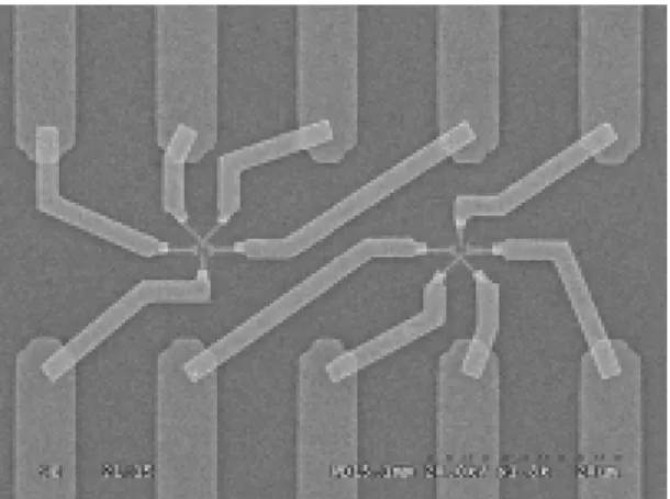
Figure 3. SEM image of two quantum dot systems.
.
圖三展示在一元件內製作的二量子點,其金屬閘極從
0.25mm
×
0.25mm
的打線點
經光微影與電子束微影等多道製程,連接至
µ
m
2的
Dots
。圖四為更高倍率的放大
Dot
結構圖,上圖類似
Marcus
小組設計,兩支
AC
閘極緊鄰一邊,而下圖乃將
兩支分置左右兩邊。
1.67
µ
m
0.85
µ
m
Figure 4. Two SEM images of a quantum dot system with different arrangement of AC
pumping gates. (Top) Two AC pumping gates are next to each other. (Bottom) Two AC gates
are at the opposite sides.
除此之外,我們也針對本小組朱仲夏老師提案製作不同
top layer
的
finger gate
組態,
其中困難性在於
: (1)split gate
與
finger gate
之間的絕緣層不可有漏電,
(2)
由於電
子平均自由徑約為
10
µ
m
,
split gate
寬度有限,造成上層的
finger gate
在多對形
況下相當擁擠,
proximity effect
增添製作難度。我們採用
Pepper
小組的方法以
PMMA
曝於電子劑量下,可形成約
120nm
絕緣層,在室溫時其電阻大於
G
Ω
(
跨
split and finger gates
測量
)
,因此在低溫的漏電率更低,因可忽略。圖五為此元件
的
SEM
影像圖,正中間
25
µ
m
×
25
µ
m
的深黑色區即為絕緣
PMMA
層,在其下方
有對
split gate
(中間
0.3
µ
m
間隙)
,而上方有數對微細交錯
finger gates
(跨過
0.3
µ
m
間隙),並以二支較粗的
metal gates
連接得以分別控制
AC
電場的時變因子。理
論推算由空間的不對稱性,在無相位差下也可有抽運傳輸,因此我們對不同對的
finger gate
可作一系列對偁(等距)與不對稱(不等距)的設計。
Figure5. SEM image of 2DEG with split gates and finger gates. A PMMA insulating layer
(dark area)is sandwiched by these two layers.
Figure 6. SEM images of narrow channels with different arrangements of finger gates. (Top)
One pair of finger gate. (Bottom) Four pairs of finger gate.
圖六顯示二種不同的組態。由於線寬僅止於
70
±
10nm
,因此當對數增加時,
split
gate
寬度大約需長
1.2
µ
m
,由於以色列
Braun center of Submicron Research
的
Dr.Umansky
給的
2DEG
,
mean free path
l
~7.5
µ
m(
經
Subnikov-deHaas
振盪的
R
xx(H)
與
Hall effect R
xy(H)
測量
)
,我們得知
long channel
將造成一些
scattering
模糊其窄
通道的量子傳輸,因此盡可能避免通道長度大於
1.5
µ
m
。
在同高頻但具相位差的兩訊號產生設備設置,由學校配合款項支援購置
Agilent
E8257C(250kHz~40GHz) source generator,
另配合系上原有
HP8752C network
analyzer(250kHz~1.3GHz)
,我們可製造兩相位差高頻同調訊號
(250kHz~1.3GHz
,
phase difference
φ
can be continuously changed from -2
π
to 2
π
)
。原
0.3K
低溫系統
成功地加設置兩
SMA
端子,銜接的兩同軸電纜線獨立地經過完善
heat sink
安排
連接樣品台上樣品的
finger gates
。
HP 8752C
Network analyzer
Agilent E8257C
Source generator
V
ocos(
ω
t+
φ
)
V
ocos(
ω
t)
Figure 7. Experimental setup for two high frequency sources with same frequency and
different phases.
-0.8 -0.6 -0.4 -0.2 0.0 0.2 0.4 0.6 0.8 -0.8 -0.7 -0.6 -0.5 -0.4 -0.3 -0.2 -0.1 0.0 0.1 0.2 0.3 0.4 0.5 0.6 0.7 0.8 0.01 0.02 0.03 0.04 -8 -6 -4 -2 0 2 4 6 8 I ( p A ) DC current test 1GΩ standard (5%) 1/slope=1.013GΩ I(V=0)=-20pA resolution ~1pA I ( n A m p) V (volt)Figure 8. DC current resolution test result for our measurement system.
三、實驗數據與討論
目前使用的二維電子系統為
MBE
長成的
GaAs/Ga
1-xAl
xAs
異質結構,其結構
如圖九,
2DEG
在離表面
93nm
下方。
Surface cap GaAs 10nm
Gate barrier 37% AlGaAs 8nm
doped layer 37% AlGaAs 15nm
Spacer 37% AlGaAs 60nm
Buffer layer 1.5
µ
m
GaAs
substrate
Figure 9. Schematic diagram of a GaAs/AlGaAs heterostructure.
其橫向傳輸
R
xx(H)
展現由磁場所引起的
Landau level quantization
及在
2DEG.
中的
step-like density of states
之典型的
Subnikov-deHaas
振盪,利用此振盪週
期,可得樣品的
carrier concentration.
)
/
1
(
1
2
H
h
e
n
s∆
=
2DEG
Hall resistance R
xy(H)
也顯示出對應於
R
xx=0
的平臺。甚至在很弱磁場中我們亦可
解析出這些平臺,
Carrier concentration
也可用
Hall measurement.
計算出;從兩
者測量得出相同結果:
n=1.2
×
10
11/cm
2.
樣品之
mobility
為
1
×
10
6cm
2/Vs.
。略低於
Dr.Umansky
給的樣品數據
n=1.4
×
10
11/cm
2、
µ
=2.2
×
10
6cm
2/Vs (w/o. illumination)
。
在解決歐姆接點等問題後,
contact
電阻可控制於
100
Ω
左右,樣品於低溫下的
方塊電阻值應為數十
Ω
,我們先著重於量子窄通道的傳輸性質測量,
split gate
上
加負偏壓使
2DEG
因負電位之
depletion
限制電子運動區域。當
sweeping gate
voltage V
g,
電子通道寬度即縮減,故我們可觀察到系統由二維至準一維、甚至通
道完全封閉
(pinch off)
的傳輸行為。我們測量數個不同閘極縫隙寬
d
gap與不同通
道長度l
channel的元件,
Figure 10. SEM images of narrow channels
with different arrangements of split gates.
l
channel-0.8 -0.7 -0.6 -0.5 -0.4 -0.3 -0.2 -0.1 0.0 0 1 2 3 4 5 6 7 G( 2 e 2 /h) Vg(Volt)