國
立
交
通
大
學
電機學院 IC 設計產業研發碩士班
碩
士
論
文
在自主指令記憶體的設計中
採用迴圈暫存器來降低指令擷取流量
Reducing Instruction Fetching Traffic
Using Loop Buffer in Autonomous Instruction Memory Design
研 究 生:許裕昇
指導教授:鍾崇斌 教授
在自主指令記憶體的設計中採用迴圈暫存器來降低指令擷取流量
Reducing Instruction Fetching Traffic
Using Loop Buffer in Autonomous Instruction Memory Design
研 究 生:許裕昇 Student:Yu-Sheng Shu
指導教授:鍾崇斌 Advisor:Chung-Ping Chung
國 立 交 通 大 學
電機學院 IC 設計產業研發碩士班
碩 士 論 文
A ThesisSubmitted to College of Electrical and Computer Engineering National Chiao Tung University
in partial Fulfillment of the Requirements for the Degree of
Master in
Industrial Technology R & D Master Program on IC Design
January 2009
Hsinchu, Taiwan, Republic of China
在自主指令記憶體的設計中採用迴圈暫存器來降低指令擷取流量
學生:許裕昇 指導教授:鍾崇斌 博士
國立交通大學 電機學院產業研發碩士班
摘 要
自主指令記憶體的設計的想法在於結合動態分支預測器和最上層的指令記憶體而 擁有自行產生指令位址的特性,因而使得 CPU 可以不用傳送指令位址給自主指令記憶 體,而達到降低 CPU 和自主指令記憶體之間指令位址匯流排上傳遞資料量的目的。而 在此種架構之下,雖然指令位址匯流排上所傳遞的資料量已經被有效的降低,然而在同 時指令內容匯流排上還是在每個時脈週期傳送著資料。因此我們的問題便是在於如何在 此種架構之下去降低 CPU 和指令記憶體以及動態分支預測器之間的指令內容匯流排上 傳遞資料量的問題。 而為了解決這樣的問題,我的想法是在 CPU 的內部增加一個緩衝器用來儲存過去 使用過的指令,而這個緩衝器不能有標誌的部分,主要的原因在於不想增加過多額外的 硬體成本。CPU 藉由存取存放於緩衝器中的指令達到節省 CPU 和自主指令記憶體之間 指令內容匯流排耗電的目的。 我們的設計將會包含了新增的輔助硬體以及一套適用於 CPU 和指令記憶體以及動 態分支預測器之間的傳輸協定,這套傳輸協定必須能夠同時達到可以有效率地控制指令 內容匯流排以及維持程式流程的正確性。 以上述的想法做為出發,我的設計將會以 line buffer 做為此種緩衝器的初步設計, 之後結合田濱華的 loop buffer 設計做更進一步的改良,最後再採用藉由指令內容匯流排 來傳送存取緩衝器中的指令的想法來使得 CPU 之中的緩衝器可以儲存巢狀迴圈進而提 升緩衝器的使用率使得指令內容匯流排的存取次數可以持續地下降。除此之外我們並目 針對當這兩條特定用途的匯流排結合成一條的通用匯流排時對於整體系統效能所造成 的影響進行評估。Reducing Instruction Fetching Traffic
Using Loop Buffer in Autonomous Instruction Memory Design
Student: Yu-Sheng Shu Advisor: Dr. Chung-Ping Chung
Industrial Technology R & D Master Program of
Electrical and Computer Engineering College
National Chiao Tung University
Abstract
The idea of Autonomous Instruction Memory (AIM) is to combine Top-Level
Instruction Memory (TLIM) and Branch Target Buffer (BTB). This kind of architecture has an character of self-generating instruction address. With this character, CPU core needs not to transfer instruction address to AIM, and this will obtain the goal of reducing traffic on
instruction address bus. Under this kind of architecture, although the traffic on instruction address bus has been greatly reduced, the instruction content bus between CPU core and AIM still works every clock cycle. Therefore, our problem is to reduce the traffice on instruction content bus between CPU core and AIM.
Our primitive idea for solving this problem is to introduce a tagless buffer inside CPU core storing those used instructions. CPU core can access instructions inside buffer instead of fetching from instruction content bus and then power consumption on instruction content bus can be saved.
Our design will including additional auxiliary hardware, buffer inside CPU core, and an efficient control bus communication protocol between CPU core and TLIM plus BTB and instruction memory are essential to maintain which instructions can be write into buffer and when to reuse these instructions.
Based on the above ideas, I will use line buffer as a first design. And then integrate loop buffer as my second design. Finally we use instruction content bus to deliver the buffer access position as my third design. Under this design, the buffer inside CPU core can store the nested loop and reuse them. Therefore, the access time of instruction content bus can continuously be reduced. Besides, we evaluate the efficiency impact if we merge the two dedicated bus into a common bus.
誌謝
終於結束了漫長的碩士求學生涯,這四年的求學生涯對我來說會是一個永生難忘的 經歷,而在此要跟長期陪伴我度過這段時間的所有人說一聲謝謝。 首先感謝我的指導老師 鍾崇斌老師,在他的諄諄教誨、辛勤指導與勉勵下,而得 以順利完成此論文。同時也感謝是我的口試委員的單智君老師、金仲達老師、鍾葉青老 師,由於他們的建議,使得這篇論文能更加完整。 感謝楊惠卿學姊全程的協助,給我很多的幫助。也感謝 jojo 學長、吳奕緯學長、延 羲、柏頤、群旻、華鼎、柏仁、勁霖、冠穎的幫助,給我很多意見及鼓勵。 最後感謝我的家人和女朋友,謝謝你們在背後全心全意的支持我、關懷我、鼓勵我。 讓我在這求學的路上走的更順利,使我能堅持追求自己的理想。 所有支持我、勉勵我的師長與親友,奉上我最誠摯的感謝與祝福,謝謝你們。List of Contents
中文摘要 ………i 英文摘要 ………ii 誌謝 ………iii 目錄 ………iv 表目錄 ………vi 圖目錄 ………viii 一、 Introduction………1 1.1 Motivation………2 1.2 Objective………41.3 Organization of this Thesis………4
二、 Background & Related Work………5
2.1 Intelligent Autonomous Instruction Memory………5
2.1.1 Mechanism of iAIM………5
2.1.2 Control Signal between CPU core and iAIM………6
2.1.3 Block Diagram of iAIM………8
2.2 Line Buffer………9
2.3 Loop Buffer………11
2.3.1 Basic Idea of Loop Buffer………11
2.3.2 Loop Buffer with Forward Branch………13
2.4 Nested Loop Buffer………14
三、 Design of Proposed Architecture……… 1 9 3.1 Proposed Design of AIM with Loop Buffer………19
3.1.1 Challenges in Design………19
3.1.2 Key Ideas in Design………20
3.1.3 My Proposed Design………20
3.2 Proposed Design of AIM with Modified Loop Buffer………21
3.2.1 Analysis of Nested Loop Backward Branch Miss Prediction Behavior…21 3.2.2 Key Ideas in Design………24
3.2.3 My Proposed Design………25
3.3 Proposed Design of Multiplex Bus under AIM with Modified Loop Buffe27 3.3.1 Multiplex Bus under Single Cycle Instruction Fetch Architecture………28
3.3.2 Multiplex Bus under Multiple Cycle Instruction Fetch Architecture……31
四、 Evaluation and Discussion………35
4.1 Evaluation Methodology………35
4.3 Experimental Environment………38
4.4 Experimental Benchmark………40
4.5 Experimental Results and Discussion………42
五、 Conclusion and Future Work………47
5.1 Conclusion………47
5.2 Future Work………48
List of Figures
Fig 1.1 Block diagram of conventional architecture………3
Fig 1.2 Block diagram of my proposed architecture………3
Fig 2.1 Additional control signals between CPU core and iAIM………6
Fig 2.2 Block Diagram of iAIM………8
Fig 2.3 Block Diagram of Line Buffer………10
Fig 2.4 Memory Accessing in Different States………11
Fig 2.5 State Diagram of Loop Buffer Controller………12
Fig 2.6 Profile the Execution Time of MiBench………13
Fig 2.7-1 Code Sequence of a Nested Loop………15
Fig 2.7-2 Loop Buffer Storing Nested Loop………15
Fig 2.8 An Example of Buffering Nested Loop………16
Fig 3.1 Primitive Design Idea of AIM with Loop Buffer………20
Fig 3.2 L-Indicate control lines that AIM uses to inform CPU………20
Fig 3.3 Modified Loop Buffer State Diagram………23
Fig 3.4 Block Diagram inside AIM side for AIM with Modified Loop Buffer………25
Fig 3.5 Block Diagram inside CPU side for AIM with Modified Loop Buffer………26
Fig 3.6 Block Diagram of Multiplex Bus under AIM with Modified Loop Buffer…………28
Fig 3.7 An Example of Code Sequence………29
Fig 3.8 Data Transfer on Bus under SCIF Architecture………30
Fig 3.9 The 8-stage Pipeline Structure of the R4000………31
Fig 3.10 Data Transfer on Bus under MCIF Architecture………32
Fig 4.1 Design flow in our implementation………39
Fig 4.3 Percentage of Instruction Cache Access………42 Fig 4.4 Increasing Bit Transition Rate on Merged Instruction Bus under SCIF Architecture43 Fig 4.5 Performance Degradation under SCIF Architecture with Multiplex Bus………44 Fig 4.6 Increasing Bit Transition Rate of AIM with Modified Loop Buffer………45 Fig 4.7 Power and Area Estimation under 90 nm………45
List of Tables
Table 3.1 Nested Loop Backward Branch Miss Prediction Behavior………21 Table 3.2 Case Analysis for Selected Benchmarks………34 Table 4.1 Communication Cost between CPU and AIM………36
Chapter 1
Introduction
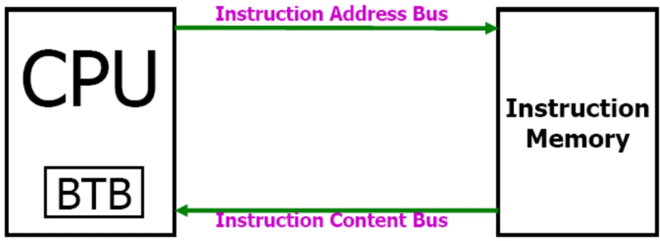
Because of memory bottle neck, modern computer architecture design will introduce TLIM (Top Level Instruction Memory) near by CPU core. And because of increasing system performance, modern computer architecture design will deploy BTB (Branch Target Buffer) for recording executed branch instructions near by CPU core. Although these two components have great contributions on releasing memory bottle neck and increasing system performance, they also occupy an immense part of CPU. Therefore, if we can move TLIM and BTB away from CPU and do not effect on the system performance, we can place other components which is more useful into CPU, EX: registers, carry look ahead adder, divider. As we move these two components away from CPU, first we will face the problem of bus power
consumption between CPU and TLIM plus BTB. Besides, we must promise the program correctness and can not drop the system performance. Under this architecture, bus between these two components can be divided into instruction address bus and instruction content bus.
Fortunately, previous research has resolved one of them. The author of [1] proposes an iAIM (intelligent Autonomous Instruction Memory) architecture which can efficiently solve the instruction address bus problem between CPU core and TLIM plus BTB. He organizes TLIM and Branch Target Buffer (BTB) as iAIM. Because of the sequential characteristic of program execution and BTB's ability of predicting branch instruction, iAIM can generate instruction address by itself and then send instruction to CPU core. Therefore, our problem can be translated to efficiently use the instruction content bus between CPU core and iAIM.
Our primitive idea for solving this problem is to introduce a tagless buffer inside CPU storing those used instructions. CPU can access instructions inside buffer instead of fetching from instruction content bus and then power consumption on instruction content bus can be saved. Furthermore, since we can greatly reduce the transferred times on both instruction address bus and instruction content bus between CPU and iAIM, we can consider further about merging these two buses into one unified multiplex bus. Therefore, we can reduce half bus demand between CPU and iAIM.
1.1 Motivation
My research comes from below four observations: 1. TLIM and BTB occupy an immense part of CPU.
If we can move these two components away from CPU, we can place other components which is more useful into CPU, such as resisters, carry look ahead adder, divider. 2. Inside [1], by proposing an iAIM architecture, the instruction address transfer times
between CPU and iAIM can be greatly reduced. During the process of instruction fetch, although the instruction address transfer times can be greatly reduced by the mechanism of iAIM, the instruction content bus between CPU and iAIM works every clock cycle.
3. Research for reducing power on instruction content bus between CPU and IM (Instruction Memory) does not appear a lot. But, many research focus on saving IM access power. In fact, the methodology for saving IM access power can also be applied to saving instruction content bus power.
4. Several kinds of methods can be used for saving IM power, like drowsy cache, cache line decay, buffering mechanism etc. For saving IM access power without affecting system performance, buffering reused instructions mechanism is a better choice.
As a conclusion, if we can propose an efficiently instruction transferring mechanism from iAIM to CPU. Then the idea of moving TLIM and BTB away from CPU can be realized. My primitive idea is to integrate the methodology of buffering repeatedly reused instructions into system with AIM. Then we can obtain a more power efficiency architecture. Furthermore, since the data transfer times on both buses have been greatly reduced, it is reasonable to
merge instruction address bus and instruction content bus into one multiplex bus. And half bus demand between CPU and IM can be reduced. Figure 1.1 and Figure 1.2 show block diagrams of conventional architecture and my proposed architecture respectively.
Figure 1.1: Block diagram of conventional architecture
1.2 Objective
As applying my design idea to iAIM architecture, total execution time and reduction in bus traffic (it includes percentage of reduced instruction content bus active cycles and percentages of reduced bit transitions) are evaluation metrics on achievement in objective. Energy conservation on instruction content bus will be evaluated from "bus active cycles" and "bit transitions on bus" metrics indirectly. The evaluation results of conventional architecture, original iAIM design and loop buffer design under the same BTB organization are given as contrasts. As to evaluating the design of merging two dedicated bus into one multiplex bus, we will evaluate the system performance impact by detecting the occurrence of transferring instruction address and instruction data at the same cycle.
1.3 Organization of this Thesis
The rest of this thesis is organized as follows. Chapter 2 will illustrate my research background. Chapter 3 explains the design detail of iAIM plus line buffer, iAIM plus loop buffer, modified iAIM plus loop buffer and multiplex bus under single cycle instruction fetch architecture or multiple cycle instruction fetch architecture. Chapter 4 presents evaluation methodology, experiment results and discussion. Conclusion and future works are then provided in Chapter 5.
Chapter 2
Background and Related Works
In this chapter, we will describe the design idea and architecture of iAIM firstly. Then we will present about the buffering mechanism for saving instruction memory access power.
2.1 Intelligent Autonomous Instruction Memory
The author of [1] organizes TLIM and BTB as iAIM. Because of the sequential
characteristic of program execution and BTB's ability of predicting branch instruction, iAIM can generate instruction address by itself and then send instruction to CPU core. Besides, the author proposes another two enhanced design. One of them equips iAIM with a partial instruction decoder capable of calculating branch target address by decoding branch
instruction. The other one equips iAIM with a partial instruction decoder and a return stack. The experiment results show three proposed designs can reduce instruction address
transmission to 97.71%, 98.49% and 99.99% and reduce total bit transitions to 84.99%, 86.54% and 92.01% compared with conventional architecture respectively. All these designs greatly outperform T0 encoding technique. The third design outperforms T0 DAT with 128 entries technique slightly.
2.1.1 Mechanism of iAIM
During program executes, it can be divided into sequential execution and taken branch execution. Sequential execution occupies about 85-90% portion of program execution, while the other occupies about 10-15%. When program executes sequentially, next instruction address comes from current instruction address plus instruction size. But when program does
not execute sequentially, next instruction address comes from complicated mechanism. And next instruction address has less relationship with current instruction address. For taken branch execution instructions, it can be divided into two categories-fixed target branches and changing target branches. Most taken branches are fixed target branches and these instructions can be handled by BTB. Therefore, the basic two ideas that iAIM can generate next
instruction address by itself are:
(1) For sequential execution instructions, with help of adder we can generate next instruction address.
(2) For fixed target taken branches, we can get branch target address with help of BTB. Under the mechanism of iAIM, those changing target branches besides procedure return will be the remainder instruction addresses that CPU core needs to transfer to iAIM.
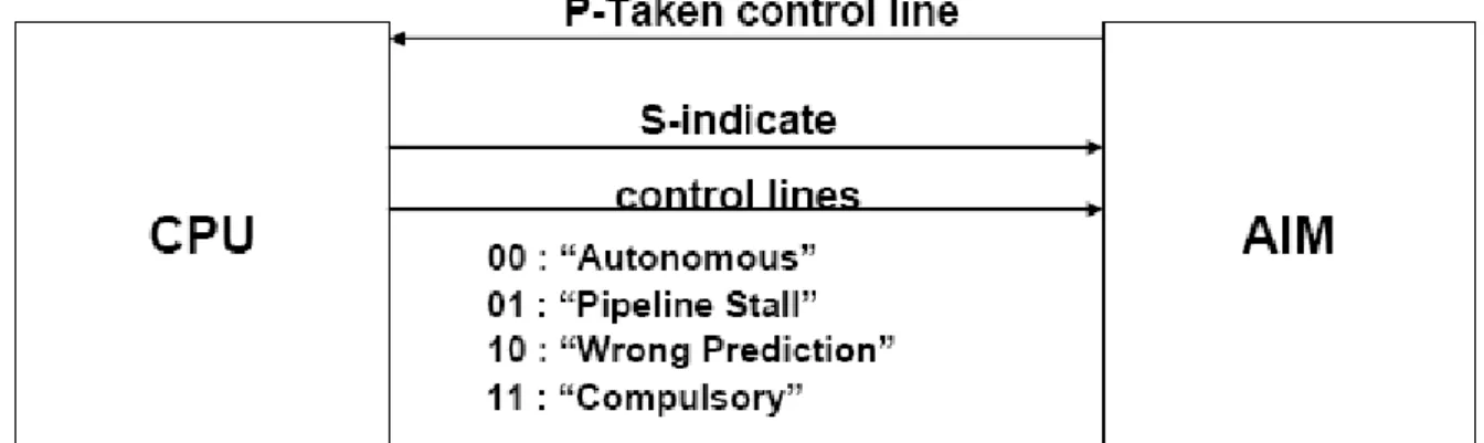
2.1.2 Control Signal between CPU core and iAIM
Although iAIM can generate most of instruction addresses by itself, there are still a few instrctuion addresses in want of CPU core transferring. And because BTB is moved from CPU core to instruction memory, the execution results of branch instruction need to be communicated between CPU core and iAIM. Therefore we need to introduce some additional control signals for transferring these messages. Additional control signals for iAIM design display as Figure 2.1.
P-Taken: (control signal from iAIM to CPU core)
P-Taken=1 : predictive taken branch was found at last clock cycle P-Taken=0 : otherwise
Because BTB is moved into iAIM, iAIM needs to tell CPU core that the branch prediction direction by BTB when taken branch happens.
S-Indicate: (control signals from CPU core to iAIM) Those messages CPU core needs to tell iAIM include:
(1) Which one instruction address should iAIM use? The instruction address generated by iAIM it self or the instruction address transferred by CPU core.
(2) When branch miss prediction happens, CPU core needs to transfer corrected instruction address to iAIM.
(3) Pipeline stall happens inside CPU core.
After appropriate encoding, we can use 2 additional control signals to generate 4 different state to transfer messages what we mention above.
Autonomous (00):
CPU will not transfer instruction address to iAIM, and iAIM will generate instruction address by itself.
Pipeline Stall (01):
CPU will stall for one clock cycle, and iAIM will send the same instruction as the previous clock cycle.
Wrong Prediction (10):
CPU detects branch miss prediction happens, and will send corrected instruction address to iAIM.
Compulsory (11):
Exception situation (including system initiates and procedure return), CPU will send instruction address to iAIM.
2.1.3 Block Diagram of iAIM
The block diagram of iAIM displays as Figure 2.2.
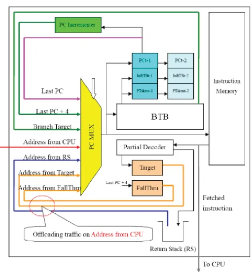
Figure 2.2: Block Diagram of iAIM
PC Incrementer is used for generating instruction address when the program is sequential execution. And BTB can give the branch target address when taken branch happens. The two 34-bit registers (PC-1(PCt-1, InBTBt-1, PTaken-1), PC-2(PCt-2, InBTBt-2, PTaken-2)) is designed for updating branch prediction result. The reason is that the actual branch execution result will be available at the 3rd stage of pipeline. The last PC on purple line comes from PC-1 works when the pipeline stall happens in CPU core. The Address from CPU on red line comes from CPU core is used for transferring instruction address when the instruction address can not be generated by iAIM itself.
Partial decoder is designed for recognizing some special instructions, like branch instruction, procedure call and procedure return. With the help of partial decoder, iAIM is able to generate the both two branch results (branch target address and fallthrough address) in time. Because of this, when branch miss prediction happens, CPU core need not to transfer the corrected branch instruction address, and what CPU core need to do is to inform the happening of the situation. Return Stack is used to save the return address of procedure return. When the program goes into a new procedure, the return address will be pushed into return stack. And when the program gets out from the procedure, the return address will be popped from return stack. With the help of partial decoder, iAIM is able to detect the happening of procedure call and procedure return. And with the existence of return stack, the return address will also need not to be transferred from CPU core. Then the traffic from CPU core can be offloaded.
2.2 Line Buffer
Several kinds of methods can be used for saving IM power, like drowsy cache, cache decay, buffering mechanism etc. But, drowsy cache [6] and cache decay [7] accompany performance degradation.
In [6], drowsy cache saves the instruction memory power by lowering supply voltages of cache lines. The contents in the cache line will not be destroyed because of the low supply voltage. But, to access the contents in the cache line will need 1-2 clock cycle because the line must be reinstated to a high-power mode. Therefore, this incurs system performance loss.
In [7], cache decay saves the instruction memory power by gating supply voltages of cache lines. The contents in the cache line are destroyed because the supply voltage is gated. The basic idea of cache decay is that before the cache lines are evicted from instruction
memory, they have a period of "dead time". The author tries to turn off these cache lines when they get into dead time. The drawback of this approach is that the state of the cache line is lost
when it is turned off and reloading it from the level 2 cache has the potential to negate any energy savings and have a significant impact on performance. Therefore, we adopt the buffer mechanism for saving IM access power.
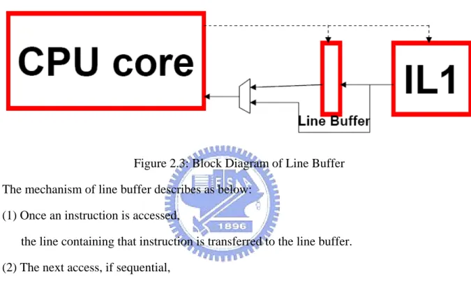
In [2], author proposed line buffer design. Line buffer is a cache line size buffer placed in front of instruction cache to capture temporal and spatial locality of reference. The block diagram of line buffer is as figure 2.3.
Figure 2.3: Block Diagram of Line Buffer The mechanism of line buffer describes as below:
(1) Once an instruction is accessed,
the line containing that instruction is transferred to the line buffer. (2) The next access, if sequential,
will be accessed from the line buffer instead of the cache.
Because of the mechanism describes above, instruction cache accessing power can be saved. The advantage of line buffer design is that instruction reusing can start quickly if the
subsequent instruction is on the same cache line.
However, the design idea of line buffer may not be appropriate for our design. The reason is that inside line buffer design line buffer need to be placed close to instruction cache. This situation accompanies high communication bus cost between line buffer and instruction cache. And this problem can be ignored inside loop buffer design because line buffer is placed close to instruction cache. However, as we introduce line buffer design idea into our design, line buffer and instruction cache are placed in two separate blocks. This contravenes the design idea of line buffer.
2.3 Loop Buffer
2.3.1Basic Idea of Loop Buffer
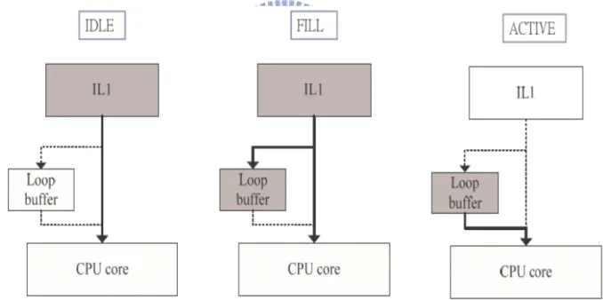
Loop buffer [3] used a tagless buffer storing those instructions inside innermost loop. Loop buffer design tries to utilizes the observation of that program execution spends most of time in loop execution. With loop buffer, CPU core can fetch instructions from loop buffer instead of instruction cache, and then instruction cache accessing power can be saved. The author of [3] introduces a 3-phase buffer managing mechanism. The whole mechanism describes as figure 2.4:
Figure 2.4: Memory Accessing in Different States
The operation status consists of three states: IDLE, FILL and ACTIVE. In the figure 2.4, the gray rectangle and the solid black line are currently accessing block and bus respectively during different states. When CPU core initializes or resets, Loop Buffer Controller (LBC) enters IDLE state first. During IDLE state, LBC detects an innermost loop. If LBC finds that the same innermost loop has been filled into loop buffer, LBC enters ACTIVE state,
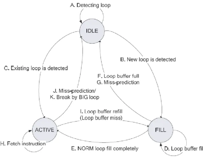
is shown in the figure 2.5.
Figure 2.5: State Diagram of Loop Buffer Controller
The transition between different basically depends on loop detection. Besides this, when branch miss prediction happens, the state will go back to IDLE state (J, G). And LBC can also handle the situation when the loop size is bigger than loop buffer size (F, K). Under this mechanism, loop buffer can be easily controlled by a few control signals. Since we need only three state to handle the access of loop buffer, the extra control signals we need will be only two. (2*2 = 4 > 3)
For meeting above state diagram, additional hardware is proposed. An extra register L_addr records the start or end address of an innermost loop been stored in loop buffer. Another register L_leng records how many instructions are stored in loop buffer when the instructions are filled into loop buffer.
2.3.2Loop Buffer with Forward Branch
Inside previous loop buffer design [3], loop buffer can only handle innermost loop. For those innermost loops containing forward branch or procedure call, loop buffer can only buffer those instructions till the happening of forward branch or procedure call. Those instructions after forward branch or procedure call must be fetched from instruction memory without reusing. This greatly reduces the efficiency of loop buffer.
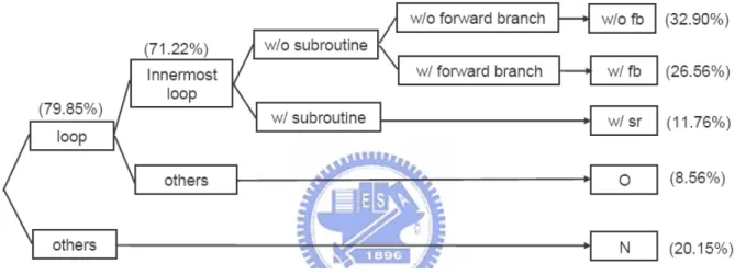
Figure 2.6: Profile the Execution Time of MiBench
As figure 2.6 shows, only 32.90% of the whole program can be completely buffered into loop buffer. And about 38.32% of the whole program cannot be completely filled into loop buffer. If this problem can be solved, the efficiency of loop buffer will be greatly improved.
According to this, many ideas are proposed to solve this problem. Nevertheless, on design complexity dictates most loop buffer designs to store only innermost loops without forward branch or instructions within innermost loops before a forward branch or procedure call. [4] proposes a simple and effective way to cope with this complexity. Author supposes that BTB is a norm in most designs, if we add an extra bit in BTB, indicating if the loop buffer stores the fall-through or target trace after a within-the-innermost-loop forward branch,
then much of the complexity can be avoided.
To store no-loop-inside subroutine in loop buffer, loop buffer must handle about the situations of procedure call and procedure return. The basic idea of handling subroutine return is to fill but disregard these invalid instructions followed with subroutine return. Since a subroutine return is an always-taken branch, CPU core will fetch G invalid instructions. According to when the subroutine return is detected by CPU core, G has two different values:
(1) G is number of pipeline stages between IF and EXE; and
(2) G is number of pipeline stages between IF and instruction decoder (ID).
However, these invalid instructions would be automatically flushed by CPU core and do not affect the correctness of program. If we store G invalid instructions into loop buffer, the instruction fetch sequence is held. This makes loop buffer can store forward branch or procedure call inside innermost loop.
2.4 Nested Loop Buffer
If we observe figure 2.6 more closely, it will have about 8.56% of the whole program we can still improve. The problem is handling nested loop inside loop buffer. The author of [5] observes that the use of backward branch (BB) instructions of a nested loop has the
characteristics of "First in, Last out" just like the using characteristics of stack. The use of BB of a nested loop is:
After the program executes once the BB of outer loop, the program must execute completely those BB inside the outer loop. Then the program will execute this BB again.
The mechanism of applying nested loop to a stack is as follows.
When a loop enters, BB instruction will be pushed to the top of stack. When the loop exits, this BB instruction will be popped from the stack.
Each entry inside stack will contain 5 components:
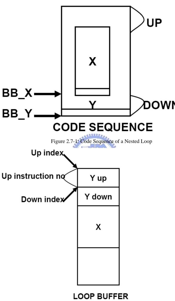
BB instruction address, fill bit, up index, down index, up instruction no. As figure 2.7-1 and figure 2.7-2:
Figure 2.7-1: Code Sequence of a Nested Loop
Fill bit:
For recording if the segment between the exit of inner loop and the exit of the adjacent outer loop is filled in buffer
Up/Down index:
For pointing out where the up/down of loop body is storing inside loop buffer Up instruction no:
For recording the instruction count of up part of loop body stored inside loop buffer An example for illustrating how to use a stack and stack entries to control the buffering of a nested loop shows in Figure 2.8.
Before we present this example, we first define some notations. S(L) means the
processor is executing the backward branch instruction of the closest loop L and the next state of the Loop Buffer Controller is S, where S = {I(IDLE), F(FILL), A(ACTIVE)}, top points to the top of the stack. X and Y stand for nested loop as shown inside Figure 2.7-1.
This example begins with an IDLE state and top is 0 as shown in Figure 2.8(a). When an backward branch instruction BB_X of loop X is detected the first time, the controller enters the FILL state and pushes the address of BB_X to stack as shown in Figure 2.8(b). The value of fill is set to 0 because instructions of loop X are not filled to buffer yet. In FILL state, the loop of X is executed in the second iteration and the instructions are buffered. When BB_X is executed the second time, the address on top of stack is compared with PC. Since they are identical, this BB_X instruction becomes a triggering backward branch instruction. The state of controller is set to ACTIVE and the fill bit is set to 1 as shown in Figure 2.8(c). In the subsequent iterations, the controller remains in ACTIVE state till BB_X instruction is executed and found to be not-taken, i.e. loop X exits. When the processor exits from loop X, the pop operation to the stack is performed. The result is shown in Figure 2.8(d).
When the backward branch instruction BB_Y, at the end of loop Y is executed the first time, the address of BB_Y instruction is pushed to the top of stack and the state of the controller is transferred to FILL state as shown in Figure 2.8(e). Since loop Y is not filled to buffer yet, the value of fill is set to 0. When the loop X in loop Y is executed the second time and BB_X in loop X is executed the second time, we know that loop X is already in the buffer. Hence, the value of fill is set to 1 and the state is transferred to ACTIVE state as shown in Figure 2.8(f). When loop X exits, the stack is popped. At the same time, the controller will check if the value of top-1 equals 0. If not, it means that there is a nesting loop and the controller will check if the fill field of top-1 of the stack is 0 (not filled) or 1 (already filled). Since the value is 0, the controller will enter FILL state as shown in Figure 2.8(g) and the segments between BB_X and BB_Y will be filled in buffer. When BB_Y is executed the second time, its address is compared with the top stack and found to be equal. This backward
branch instruction becomes triggering backward branch and the controller goes to ACTIVE state. Since loop Y is already in buffer, the fill field is set to 1 as shown in Figure 2.8(h). When loop Y exits, the top of stack is popped as shown in Figure 2.8(i).
Chapter 3
Design of Proposed Architecture
In this chapter, we propose our architecture. In section 3.1 we present the architecture of AIM with loop buffer. In section 3.2 we present the architecture of AIM with modified loop buffer for handling nested loop problem. In section 3.3 we describe the architecture of merging instruction address bus and instruction content bus into unified multiplex bus under single cycle instruction fetch architecture and multi-cycle instruction fetch architecture.
3.1 Proposed Design of AIM with Loop Buffer
3.1.1Challenges in Design
When loop buffer is added into CPU core for saving IM power, problems of buffer maintenance and instruction content source choice are introduced and need to be solved. These problems arise from separated loop buffer and loop buffer controller. To integrate loop buffer into system with AIM for saving instruction content bus power, loop buffer have to be allocated inside CPU core. And loop buffer controller need to be allocated inside AIM because it need to get branch information coming from BTB plus control IM access and instruction content bus activity. The problem of buffer maintenance means buffer controller need to enter, update buffer entries inside CPU core. And the problem of instruction content source choice means that CPU core need to know when to use the previous saved instruction inside buffer and when to use the value on Instruction Content Bus prepared by AIM.
3.1.2Key Ideas in Design
For overcome the design challenges proposed inside previous section, our primitive design idea is to add additional control buses and to design an efficient communication protocol. This shows in Figure 3.1.
Figure 3.1: Primitive Design Idea of AIM with Loop Buffer
3.1.3My Proposed Design
Based on the ideas proposed in previous section and the ideas proposed in loop buffer [3], to integrate loop buffer into system with AIM, what we need to do is to increase 2 additional control lines to indicate the loop buffer state.
As Figure 3.2 shows, 2 control lines from AIM to CPU for AIM to inform CPU one of 3 kinds of situations (called "Loop Buffer Situation Indication" or "L-Indication" control lines):
00 for IDLE
CPU fetches instructions from AIM 01 for FILL
CPU fetches instructions from AIM and also CPU fills instructions into loop buffer 10 for ACTIVE
CPU fetches instructions from loop buffer
3.2 Proposed Design of AIM with Modified Loop Buffer
3.2.1Analysis of Nested Loop Backward Branch Miss
Prediction Behavior
For loop buffer with the ability to access nested loop, we propose the modified design. At first we analyze the nested loop backward branch miss prediction behavior. As Table 3.1 shows.
Loop type: Outer loop / Inner loop
Outer loop: The outerest loop detected by loop buffer controller Inner loop: Other loop containing inside outer loop
WP (Wrong Prediction) type: NTÆT / TÆNT
NTÆT: BTB predicts branch as a not taken branch, but the branch execution result is taken. TÆNT: BTB predicts branch as a taken branch, but the branch execution result is not taken.
FILL / REUSE:
How CPU core handles the following instructions?
FILL: CPU core will fetch instructions from instruction content bus and write instructions into loop buffer.
REUSE: CPU core will fetch instructions from loop buffer.
This table is partitioned by loop type, branch miss prediction type and the handling of CPU core fetching instructions. And the row of Table 3.1 should be 8 rows at first, not 6 rows what we present here. It is because that these 2 rows will not happen anymore. Therefore we cancel these 2 rows at last.
The first row we cancel here is the row (Inner, NT-->T, FILL). We cancel this row here because inner loop instructions will have been filled into loop buffer previously when we detect the branch miss prediction of inner loop. These instructions are filled previously when outer loop is filled into loop buffer. Loop buffer controller will find out where the branch target instruction is allocated.
The second row we cancel here is the other row of (Outer, T-->NT). It is because when we detect the problem has exited from nested loop, CPU core can only fetch instructions from instruction memory.
A new state of loop buffer state diagram is introduced here-INDEX_ACTIVE. INDEX_ACTIVE state is used to tell CPU reading index from instruction content bus and using it to find out instructions from loop buffer. For loop buffer only storing innermost loop, CPU core can fetch instructions from loop buffer sequentially. But for loop buffer storing nested loop, CPU core need to fetch instructions from loop buffer randomly. Only the loop buffer controller knows how these instructions are stored inside loop buffer. The idea of INDEX_ACTIVE state will be explained in the following section.
According to Table 3.1, we propose a modified loop buffer state diagram as Figure 3.3. Inside this diagram, we hide the existed state transition descriptions. We only show those state transitions come from handling nested loop.
3.2.2Key Ideas in Design
Two ideas for we can store nested loop inside loop buffer will introduce here. The first idea is loop buffer index. Loop buffer index is used to index the access location of loop buffer, and is sent by AIM. For loop buffer with the ability to access nested loop, CPU core has the difficulty in fetching reused instructions from loop buffer. With the help of loop buffer index, CPU core can know where to fetch instructions from loop buffer. The notion of loop buffer index is:
When CPU gets instructions from loop buffer, the instruction content bus is free to use.
Therefore, we can use instruction content bus to send the loop buffer index.
With this notion, loop buffer controller can ask CPU core to fetch instructions from any locations of loop buffer without increasing extra hardware. But, we still need to use this notion carefully. It is because that the use of loop buffer index also means bit transitions on instruction content bus. Therefore, we only use this notion when the program sequence changes.
The second idea is the additional state: INDEX_ACTIVE state. INDEX_ACTIVE state is used to tell CPU reading index from instruction content bus and using it to find out
instructions from loop buffer. For loop buffer with the ability to access nested loop, CPU core has the difficulty in fetching reused instructions from loop buffer. The idea of loop buffer index is to use instruction content bus sending the access location of loop buffer. But, we still need to do some modifications on the buffer managing mechanism. To help CPU core
knowing where to fetch next instructions when this instructions storing inside loop buffer. Although we introduce an extra state, the algorithm still keeps invariable. Because the extra state is just used to tell CPU where to fetch the next instruction, it is still reusing instructions from loop buffer (ACTIVE state).
3.2.3My Proposed Design
Figure 3.4 shows the block diagram inside AIM side for AIM with modified loop buffer design. LBC stands for Loop Buffer Controller. LS stands for Loop Stack. Lines and blocks in blue mean new components different from previous AIM design.
Figure 3.4: Block Diagram inside AIM side for AIM with Modified Loop Buffer
Loop stack is responsible for handling nested loop. Each entry inside loop stack contains backward branch instruction address, fill bit, and the length of instructions storing inside loop buffer. Fill bit records if the segment between the exit of inner loop and the exit of the
adjacent outer loop is filled in buffer.
AIM controller receives S-Indicate (S0, S1) and instruction address from CPU core and generates correct instruction address for LBC and instruction memory. AIM controller receives branch information from BTB and is responsible for updating it inside BTB. After receiving instruction address from AIM controller and branch information from BTB, LBC decides how to send instructions to CPU core based on the state diagram showing inside
Figure 3.3. LBC uses L-Indicate to inform CPU core where to fetch the next instructions as previous section describes. LBC will also disable the instruction memory when CPU core fetch instructions from loop buffer.
Figure 3.5: Block Diagram inside CPU side for AIM with Modified Loop Buffer
Figure 3.5 shows the block diagram inside CPU side for AIM with Modified Loop Buffer. SR stands for State Register. State register locates in loop buffer controller inside CPU and is used to handle different branch prediction results between CPU and AIM. State register is composed of 2 bits loop state (l0, l1) and 1 bit bpr (branch prediction result). Loop state bits are used to remember the last cycle's loop state delivered by AIM from L-Indication control signals. Bpr bit is used to remember the branch prediction result delivered by AIM from P-Taken control signal. With the help of state register, CPU is able to distinguish miss prediction directions (forward branch or backward branch), miss prediction types (taken to not taken or not taken to taken), loop types (inner or outer).
LBC inside CPU receives L-Indicate and instruction from AIM and according to the state L-Indicate shows decides where to fetch next instruction. LBC will disable the access of loop buffer when the loop buffer state is under IDLE state.
3.3 Proposed Design of Multiplex Bus under AIM with
Modified Loop Buffer
Through the above architecture what we propose, the transmission times on instruction content bus between CPU and AIM can be greatly reduced. And the purpose of AIM is
focused on reducing the transmission times on instruction address bus between CPU and AIM. Since the transmission times on instruction content bus and instruction address bus under the architecture of AIM with modified loop buffer have become sufficient few, we attempt to merge these two buses into one multiplex bus.
The advantage of using multiplex bus under system with AIM plus modified loop buffer is that half bus during instruction fetching between CPU and AIM can be saved and the static power due to this bus can also be saved. But, one problem emerging from the using of
multiplex bus is that system performance may reduce. The reason is when CPU and AIM need to send instruction address and instruction at the same clock cycle, AIM needs to wait one clock cycle until CPU completes the transmission of instruction address. We call this as bus contention. Although the transmission times of instruction address are greatly reduced due to the design of AIM, bus contention still happens unavoidable. The problem of bus contention is very important. This may destroy our effort on both instruction address bus and instruction content bus. As bus contention happens once, the system's total execution time will extend one clock cycle. The extension of total execution time means more power is consumed. Another problem is that after bus merging, bit transitions on multiplex bus may increase. The effect of this problem is not very great in fact. The reason is the increasing number of bit transitions is small. Then we will focus on the problem of bus contention. In the following section, we will discuss this issue inside single cycle instruction fetch architecture and multiple cycle instruction fetch architecture respectively.
3.3.1Multiplex Bus under Single Cycle Instruction Fetch
Architecture
Instruction fetch including CPU core transferring instruction address to instruction memory and instruction memory transferring instruction to CPU core. Single cycle instruction fetch (SCIF) architecture means that as CPU core fetches instructions from instruction
memory, this takes one clock cycle. Therefore, multiple cycle instruction fetch (MCIF) architecture stands for the fetching time of CPU core getting instructions from instruction memory more than one clock cycle. Conventional computer architecture adopts the SCIF design. As we adopt the idea of multiplex bus into our AIM with modified loop buffer design under SCIF architecture, the issue of bus contention is unavoidable. The advantage of our design for adopting multiplex bus is that for reducing instruction address transferring times AIM performs better than other design. Therefore this can reduce the happening of bus contention. Figure 3.6 shows the block diagram of our design. With one additional control signal (multiplex bus direction), CPU core can tell AIM when to receive instruction address from multiplex bus and when to transfer instruction through multiple bus according to if CPU core needs to transfer instruction address.
Figure 3.7: An Example of Code Sequence
Here we use an example to illustrate the data transferring on instruction address bus, instruction content bus and multiplex bus under different instruction fetching architecture. Figure 3.7 is a code sequence example. Each row is a pair of instruction address and
instruction. And the green one is a branch instruction while the yellow one is the branch target instruction of this branch instruction. The environment is a 5-stage pipeline with IF
(instruction fetch), ID (instruction decode), EX (execution), MEM (memory) and WB (write back). And the branch prediction result will produce in ID stage.
While CPU core executes the code sequence in Figure 3.7, a forward branch miss prediction happens. Figure 3.8 shows how data transferring on different bus environment under SCIF architecture. Inside the picture of "Seperate IAdrs bus and ID bus", TX stands for the current clock cycle. Red line stands for instruction address bus while instruction address in red locates above this red line. Blue line stands for instruction bus while instruction in blue locates above this blue line. Inside the picture of "Unified Multiplex Bus", Light blue line stands for multiplex bus.
Figure 3.8: Data Transfer on Bus under SCIF Architecture
Under the system using separate instruction address bus and instruction data bus, after CPU core receives branch instruction at 11 clock cycle, the branch result is calculated at 12 clock cycle. And at 13 clock cycle CPU core sends the corrected instruction address to AIM, then AIM transfers the corresponding instruction back to CPU core. The miss penalty is 1 clock cycle.
Under the system using multiplex bus, after CPU core receives branch instruction at 11 clock cycle, the branch result is calculated at 12 clock cycle. At 13 clock cycle bus contention happens, AIM needs to wait one clock until CPU completes the transmission of instruction address. This extends the miss penalty to 2 clock cycle.
Besides extending the total execution, the other issue of adopting multiplex bus under SCIF architecture is the need for additional latch. Additional latch is necessary for keeping instruction address behind the output of multiplex bus inside AIM and this will emerge two consecutive problems.
1. Latch will extend the instruction fetch time, and this will result in cycle time violation. 2. No applicable trigger in the system is able to enable latch.
3.3.2Multiplex Bus under Multiple Cycle Instruction Fetch
Architecture
For improving system performance, MCIF architecture is common in current computer architecture design. Figure 3.9 shows the 8-stage pipeline structure of the MIPS R4000 processor family. The R4000 implements MIPS64 but uses a deeper pipeline than that of conventional 5-stage design both for integer and FP programs. This deeper pipeline allows it to achieve higher clock rates by decomposing the 5-stage integer pipeline into 8 stages. Because cache access is particularly time critical, the extra pipeline stages come from decomposing the memory access. As Figure 3.9 shows. The R4000 decomposes the
instruction memory access into 2 stages while the data memory access is decomposed into 3 stages. The function of each stage is as follows:
IF: First half of instruction fetch; PC selection actually happens here. IS: Second half instruction fetch.
RF: Instruction decode and register fetch, hazard checking, and also instruction cache hit detection.
EX: Execution, which includes effective address calculation, ALU operation, and branch-target computation and condition evaluation.
DF: Data fetch, first half of data cache access.
DS: Second half of data fetch, completion of data cache access. TC: Tag check, determine whether the data cache access hit. WB: Write back for loads and register-register operations.
Under MCIF architecture applying multiplex bus under AIM with modified loop buffer can obtain the benefits of saving power consumption and avoid the problems emerging out of SCIF architecture. The bus contention issue will disappear under MCIF architecture because of the characteristic of AIM. That is merging bus under MCIF architecture with design of AIM with modified loop buffer will not cause performance degradation.
The idea is that under MCIF architecture when bus contention happens, the instruction that AIM needs to transfer can be abandoned. Therefore miss penalty keep invariance and performance degradation disappears. The reason is that under the system with AIM as CPU core needs to transfer instruction address to AIM, it means the program flow changes. Since the result of branch will calculated at pipeline's third stage and the instruction transferring from AIM is 1 clock cycle age under MCIF architecture, the instruction that AIM needs to transfer is useless and can be abandoned.
Here we use an example to explain the idea mentioned above. Figure 3.10 shows how data transferring on different bus environment under MCIF architecture. The code sequence is the same as Figure 3.7. Under the system using separate instruction address bus and
instruction data bus, CPU core receives branch instruction at 12 clock cycle, the branch result is calculated at 13 clock cycle. At 14 clock cycle CPU core sends the corrected instruction address to AIM, and AIM still transfers the wrong instruction to CPU core. The corrected instruction will be received by CPU core at 15 clock cycle. The miss penalty is 2 clock cycle.
Under the system using multiplex bus, after CPU core receives branch instruction at 12 clock cycle, the branch result is calculated at 13 clock cycle. At 14 clock cycle bus contention happens, and the wrong instruction transferred by AIM is abandoned. The corrected
instruction is still received by CPU core at 15 clock cycle. The miss penalty holds on 2 clock cycle.
Here we verify our ideas by checking all possibly happening cases on multiplex bus. Under our system with AIM plus modified loop buffer, the data transmission times from CPU core are greatly less than those from AIM. Therefore, we analysis the behavior of CPU core transferring instruction address.
As section 2.1 mentioned, with combining BTB, AIM can generate sequential instruction address and branch target address by itself. By the help of partial decode, AIM is able to generate corrected instruction address as branch miss prediction happens. With partial decode, AIM can save return address of procedure return. Through these mechanisms, the
transmission times of CPU core transferring instruction address can be reduced to 0.1% compared to the conventional architecture. At last, three kinds of instruction addresses still need to be transferred by CPU core under our system.
1.INITIAL: The 1st instruction address as program starts. 2.JR_OTHER: Jump to register that is not link register. 3.JALR: Jump and link register
The instruction addresses of type 2 and type 3 have not fixed branch target address and can not be calculated previously. They must be supplied by CPU core. Table 3.2 shows the details what we mention above.
total instruction count INITIAL JR_OTHER JALR basicmath 60104486 1 40693 19753 bitcount 47555290 1 37 39 jpegdecode 38965 1 42 59 jpegencode 43520 1 44 59 lame 246729 1 37 59 dijkstra 29067 1 3 17 stringsearch 214676 1 116 77 rijndaeldecrypt 20825 1 5 23 rijndaelencrypt 20822 1 5 23 sha 16655 1 5 23 adpcmedecode 31112964 1 1403 1418 adpcmencode 38689120 1 1404 1419 CRC32 19059 1 8 24 FFT 18740927 1 210 125 FFTinverse 16194643 1 172 106
Chapter 4
Evaluation and Discussion
Proposed designs in Chapter 3 are evaluated by trace-driven simulator. The benchmark suit is a subset of MiBench [9], which is a benchmark suite for embedded programs. The results are evaluated by four metrics: total execution cycles, percentage of resident bit
transitions on instruction content bus, percentage of resident instruction cache access rate, and percentage of increased bit transition on multiplex bus
4.1 Evaluation Methodology
Since proposed designs in Chapter 3 are system-level innovation in computer
architecture, behavioral simulation like trace-driven simulator can be a suitable approach to prove how many benefits such innovation gains compared with other architecture.
Proposed designs are evaluated by a trace-driven simulator. Since proposed designs in this thesis are based on classic MIPS five-stage pipeline, my simulator uses MIPS I
instruction trace as key input.
My trace-driven simulator accepts the following parameters as its input:
1. Architecture: AIM, AIM with line buffer, AIM with loop buffer, proposed design of AIM with modified loop buffer, and proposed design applying multiplex under SCIF/MCIF architecture
2. Loop buffer size: 4, 8, 16, … , 1024
3. MIPS I instruction trace of benchmark program
My trace-driven simulator will records bit transitions for every line of instruction content bus and additional control lines (original AIM architecture has no additional control line;
AIM with line buffer has 1+N additional control lines (N depends on line buffer size); AIM with loop buffer and my proposed design have 2 additional control lines, and my proposed design applying multiplex bus has 3 additional control lines.) at every clock cycle during MIPS I instruction trace is being fed. We summarize these in Table 4.1.
Table 4.1: Communication Cost between CPU and AIM
After finishes execution, my simulator will output the following data: 1. Total execution cycles
2. Instruction address bus active cycles
3. Total bit transitions on instruction address bus and control line (s) 4. Instruction content bus active cycles
5. Total bit transitions on instruction content bus and control line (s) 6. Multiplex bus active cycles
7. Total bit transitions on multiplex bus and control line (s)
After collecting all statistics of selected benchmark programs, we have enough data to do evaluation on proposed designs. The evaluation metrics are listed in next section.
4.2 Evaluation Metrics
In this thesis, the following metrics are used to evaluate proposed designs of AIM: z Total execution cycles
This metric is used to indicate whether proposed multiplex bus designs suffer performance loss due to longer execution time compared with original AIM architecture.
z Percentage of resident bit transitions on instruction content bus This value is defined as:
(Total bit transitions on instruction content bus) / (Total bit transitions on instruction content bus in conventional architecture)
If this value is low, it means number of bit transitions on instruction content bus is small. This metric can effectively be used to evaluate bus power consumption indirectly due to self-capacitance.
z Percentage of resident instruction cache access rate This value is defined as:
Instruction content bus active cycles / Total execution cycles
If this value is low, it means instruction cache is disabled most of the time. Under system with buffering instruction mechanism inside CPU core, if AIM need not to transfer instructions to CPU core, it means that instructions need not to transferred through instruction content bus and instruction cache need not to be accessed. Here we only show the instruction cache access times because instruction cache
consumes more power than instruction content bus. z Percentage of increased bit transitions on multiplex bus
This value is defined as:
instruction address bus and control lines + Total bit transitions on instruction content bus and control lines)
If this value is high, it means increasing number of bit transitions on multiplex bus is great. This metric can effectively be used to evaluate bus power consumption indirectly due to self-capacitance. Although multiplex bus can reduce the
communication cost between CPU core and AIM by half, it might incur increasing bit transitions on multiplex bus compared with dedicated bus. Here we have to verify that these increasing bit transitions is very small, therefore it will not counteract our effort on multiplex bus.
4.3 Experimental Environment
The experimental toolset MIPS SDE / MIPS FGT 5.02.02 [10] is used to generate MIPS I instruction trace for benchmark programs :
z Install MIPS SDE / MIPS FGT 5.02.02.
z Use command “sde-make SBD=GSIM1B” to build MIPS I code (benchmark_ram) of benchmark program for GNU simulator platform.
z Use command “sde-run --trace-insn=on --trace-file trace_filename benchmark_ram” to generate MIPS I instruction trace file.
Since delay branch slot is always applied in GNU simulator platform, the generated trace file needs to be modified to remove delay branch slot for all branch and jump instructions. The modified trace file is then fed into trace simulator by specifying various parameters like BTB configuration (perfect BTB or not, the number of entries/set-associativity/replacement algorithm of BTB), return stack configuration (return stack is used or not), and selected design (AIM, AIM with line buffer, AIM with loop buffer, proposed design of AIM with modified loop buffer, and proposed design applying multiplex under SCIF/MCIF
4.4 Experimental Benchmark
The benchmark programs selected are a subset of MiBench [9], which is a benchmark suite consisting of commercially representative embedded programs. MiBench consists of 6 categories including Automotive and Industrial Control, Network, Security, Consumer Devices, Office Automation, and Telecommunications. In each category, at least one
benchmark is chosen as experimental benchmark. All chosen benchmarks are listed as below : z In the category of Automotive and Industrial Control
basicmath: it performs simple mathematical calculations that often don’t have
dedicated hardware support in embedded processors.
bitcount: it tests the bit manipulation abilities of a processor by counting the
number of bits in an array of integers. z In the category of Network
dijkstra : it constructs a large graph in an adjacency matrix representation and then
calculates the shortest path between every pair of nodes using repeated applications of Dijkstra’s algorithm.
z In the category of Security
sha : it is the secure hash algorithm that produces a 160-bit message digest for a
given input. It is often used in the secure exchange of cryptographic keys and for generating digital signatures.
rijndael encrypt/decrypt : Rijndael was selected as the National Institute of
Standards and Technologies Advanced Encryption Standard (AES). It is a block cipher with the option of 128-, 192-, and 256-bit keys and blocks.
z In the category of Consumer Devices
jpeg encode/decode : JPEG is a standard, lossy compression image format. It is a
representative algorithm for image compression and decompression and is commonly used to view images embedded in documents.
lame : it is a GPL'ed MP3 encoder that supports constant, average and variable
bit-rate encoding. It uses small and large wave files for its data inputs. z In the category of Office Automation
stringsearch : it searches for given words in phrases using a case insensitive
comparison algorithm. z In the category of Telecommunications
FFT/IFFT : it performs a Fast Fourier Transform and its inverse transform on an
array of data. Fourier transforms are used in digital signal processing to find the frequencies contained in a given input signal.
ADPCM encode/decode : Adaptive Differential Pulse Code Modulation (ADPCM)
is a variation of the well-known standard Pulse Code Modulation (PCM). A common implementation takes 16-bit linear PCM samples and converts them to 4-bit samples, yielding a compression rate of 4:1.
CRC32 : it performs a 32-bit Cyclic Redundancy Check (CRC) on a file. CRC
4.5 Experimental Results and Discussion
Figure 4.2: Percentage of Bit Transitions on Instruction Content Bus and Control Signals
Figure 4.2 and Figure 4.3 show resident ratios in instruction content bus bit transitions and instruction cache access for 3 different designs respectively under different buffer size. In Figure 4.2, my proposed design of AIM with modified loop buffer is better than the other two designs at the reduction bit transition rate of instruction content bus and control signals on different buffer sizes. And Figure 4.2 also shows that the great redundant control signals of AIM with line buffer counteract the effects on instruction content bus. In Figure 4.3, my proposed design of AIM with modified loop buffer is better than the design of AIM with loop buffer on different buffer sizes but buffer size = 8. The reason is when the buffer size is small, buffer will not be big enough to store nested loop and the refill of buffer will happen
repeatedly. Although AIM with line buffer will perform better on big buffer size, the
increasing bit transitions and extra power due to big buffer size will counteract the superiority.
Figure 4.4: Increasing Bit Transition Rate on Merged Instruction Bus under SCIF Architecture
Figure 4.4 shows percentage of increasing bit transitions on merged bus under SCIF architecture for 3 different designs respectively under different experimental benchmark. To eliminate the biased due to small or big buffer size, we adopt the average buffer size from 16 words to 64 words in Figure 4.4 and Figure 4.6. The increasing bit transitions diverge
between different benchmarks, and the design of AIM with line buffer perform a little better than other two designs. The increasing rate of bit transitions is very small after the buses are merged over the whole three designs (about 0.2%).
Figure 4.5: Performance Degradation under SCIF Architecture with Multiplex Bus
Figure 4.5 and Figure 4.6 is estimated under my proposed design (AIM with modified loop buffer). Figure 4.5 shows the percentage of performance degradation when applying multiplex bus under SCIF architecture with my proposed design. And Figure 4.6 shows the increasing bit transition rate comparison between SCIF and MCIF architecture with multiplex bus. As Figure 4.5 shows, although applying multiplex bus will incur performance
degradation, the effort is very small (about 0.1%). In Figure 4.6, the average increasing bit transition rate under MCIF architecture is better than that of SCIF architecture. It is because that when some instructions are need not to be transferred in MCIF architecture, the
Figure 4.6: Increasing Bit Transition Rate of AIM with Modified Loop Buffer (average of buffer size from 16 words to 64 words)
Figure 4.7 shows the estimation increasing power and area due to our additional loop buffer under technology node 90 nm. As Figure 4.7 shows, as buffer size bigger than 128, the area increases greatly. And as buffer size bigger than 512, the dynamic energy and static power increase dramatically.
Chapter 5
Conclusion and Future Work
5.1 Conclusion
The original goal of our research is to save power consumption on instruction content bus between CPU and AIM. In fact, saving instruction content bus power can not be separated from saving instruction memory access power. Therefore we obtain our objective by
integrating buffer mechanism into system with AIM. When the data transferred times on both instruction address bus and instruction content bus are greatly reduced, merging these two buses into one unified multiplex bus can save more power consumption. According to our experiment results, we have the below conclusions:
1. With some additional circuit, we can easily integrate buffer mechanism into system with AIM.
2. The extra power consumption due to large buffer size should be taken into account when designing.
3. With adopting the idea of multiplex bus, we can save more power due to reduction of bus hardware.
4. Multiplex bus would also incur system performance degradation, and result in additional power consumption. This may counteract the benefit of merging bus. 5. Our design would be more power efficiency under off chip instruction memory
5.2 Future Work
1. Our design of AIM with modified loop buffer starts from a system with AIM. We can use other instruction address bus power saving mechanism like T0 encoding to replace the role of AIM. This may create other more power efficiency architecture.
2. When we integrate buffer mechanism into system with AIM, we assume that buffer and buffer controller should be placed separated inside CPU core and AIM. If buffer and buffer controller are both placed inside CPU core, the communication cost between CPU core and AIM may be reduced further. This would need to design new communication mechanism.
References
[1] L. M. Wang and C. P. Chung, “Intelligent Autonomous Instruction Memory Design”, 2006
[2] K Ali, M Aboelaze, S Datta, “Predictive Line Buffer: A fast, Energy Efficient Cache Architecture”, SoutheastCon, Proceedings of the IEEE, 2006
[3] L. H. Lee, B. Moyer, and J. Arends, “Instruction fetch energy reduction using loop caches for embedded applications with small tight loops”, In Intl. Symp. on Low Power Electronics and Design, Aug. 1999
[4] B. H. Tein and C. P. Chung, “Power Reduction in Instruction Fetch Using Forward-Branch and Subroutine Bufferable Innermost Loop Buffer with Assistance of BTB”, 2006
[5] Wu, C.T., and Hwang, T.T., “Instruction buffering for nested loops in low power design”, in Proc. ISCAS'2002 , vol. 4, pp. 81–84, Scottsdale, Ariz, USA, May 2002 [6] K. Flautner, N. S. Kim, S. Martin, D. Blaauw, and T. Mudge, “Drowsy caches:
Simple techniques for reducing leakage power, In Proceedings of the 29th Annual International Symposium on Computer Architecture”, pages 147–57, May 2002. [7] S. Kaxiras, Z. Hu, and M. Martonosi, “Cache decay: Exploiting generational
behavior to reduce cache leakage power”, Proc. of Int. Symp. Computer Architecture, pp. 240-251, 2001
[8] J. L. Hennessy and D. A. Patterson, “Computer Architecture - A Quantitative Approach”, 2003
[9] M. Guthaus, J. Ringenberg, D. Ernst, T. Austin, T. Mudge, and R. Brown,
“MiBench: A Free, Commercially Representative Embedded Benchmark Suite”, In IEEE 4th Workshop on Workload Characterization, Dec. 2001
[10] MIPS Technologies, Inc., “MIPS SDE / MIPS FGT 5.02.02 Programmers’Guide”, 2003