國 立 交 通 大 學
電信工程研究所
碩 士 論 文
用以激發電路板輻射地緣電流之
新微波元件:輻射電流驅動器
A New Microwave Component (Current Driver)
for Inducing Radiating Ground Edge Current in a
Printed Circuit Board
研究生:劉財溢
(Tsai-I Liu)
指導教授:鍾世忠 教授
(Dr. Shyh-Jong Chung)
用以激發電路板輻射地緣電流之
新微波元件:輻射電流驅動器
A New Microwave Component (Current Driver) for Inducing
Radiating Ground Edge Current in a Printed Circuit Board
研究生:劉財溢 Student : Tsai-I Liu
指導教授:鍾世忠 博士 Advisor : Dr. Shyh-Jong Chung
國立交通大學
電信工程研究所
碩士論文
A Thesis
Submitted to Institute of Communication Engineering
College of Electrical and Computer Engineering
National Chiao Tung University
in Partial Fulfillment of the Requirements
For the Degree of Master of Science
In Communication Engineering
July 2009
Hsinchu, Taiwan, Republic of China
I
用以
用以
用以
用以激發電路板
激發電路板
激發電路板輻射
激發電路板
輻射
輻射
輻射地緣
地緣
地緣
地緣電流之
電流之
電流之
電流之
新
新
新
新微波元件
微波元件
微波元件
微波元件:
::
:輻射電流驅動器
輻射電流驅動器
輻射電流驅動器
輻射電流驅動器
研究生:劉財溢 指導教授:鍾世忠 博士
電信工程研究所
碩士論文
摘要
摘要
摘要
摘要
在本論文中,我們提出一種名為電流驅動器之新型微波元件來激發地緣輻射電 流。由於電流驅動器本身只作為一種小型的饋入裝置來將能量有效地饋入接地面產 生輻射,因此對整體輻射的貢獻量很小,所以驅動器的尺寸可以設計得十分小而不 影響整體天線特性。此種激發地緣電流作為輻射源的作法,相對於一般縮小化天線 設計來說,在大幅地減小天線設計空間的同時,也不影響整體的輻射特性。此外本 論文引用一種縮小化的巴倫等效電路模型來解釋電流驅動器的地緣電流產生機制並 用來設計電流驅動器。在論文中,我們亦針對常用於隔離電磁干擾的金屬屏蔽盒對 電流驅動器的特性影響做探討。結果指出即使在屏蔽盒緊臨電流驅動器的情況下, 對驅動器的整體特性影響也不大。這顯示出電流驅動器在小型無線裝置的設計彈 性。 基於上述的電流驅動器的優點,本論文提出二種基於電流驅動器的天線應用, 此二種架構皆製作在常用的 FR4 基板上。首先我們設計應用於 WLAN 2.4 GHz 的 電流驅動器,此驅動器可利用集總電容或者是指插式電容來實現,整體尺寸僅 4 mm × 4 mm,並具備良好的天線輻射特性。在 2.45 GHz 時,量測的天線輻射效率 大於 60 %,並且在其接近全向性的平面上,量測的平均增益接近 0 dBi。接下來, 我們藉由合併二個單頻的電流驅動器來達成雙頻 WLAN 2.4/5.2 GHz 操作,整體II 尺寸為 8.5 mm × 4 mm。我們將在論文中詳細呈現雙頻電流驅動器的設計流程。量 測的天線特性在低頻 2.45 GHz 時與先前提出的單一 2.4 GHz 的電流驅動器特性大 致相符,具有接近全向性的場型與大於 60%的天線輻射效率。而在高頻 5.2 GHz 時,由於 FR4 基板在高頻的介質損耗,量測的天線效率降低至 50%左右,但仍然 保持接近全向性的場型。實際量測結果與模擬結果相當吻合。由於利用電流驅動器 來達成天線應用具有小尺寸且具備良好的天線輻射特性等優點,因此很適合應用於 無線通訊系統。
III
A New Microwave Component (Current Driver) for Inducing
Radiating Ground Edge Current in a Printed Circuit Board
Student : Tsai-I Liu Advisor : Dr. Shyh-Jong Chung Institute of Communication Engineering
National Chiao Tung University
A
BSTRACTIn this thesis, a new microwave component named current driver is proposed, which is capable of inducing ground edge current for radiation. Since the current driver serves as a small feeding structure with little contribution to radiation, it can be designed very small while good radiation properties are maintained. Compared to the miniaturized antennas, the approach that utilizes ground plane as the main radiation has smaller size and better antenna performance. Furthermore, a circuit model of the miniaturized balun (balanced to unbalanced transformer) is introduced to explain the current inducing mechanism and to provide some valuable physical insights into the properties of the current driver. The effect of a shielding metal box for the proximity circuitry near the current driver is also investigated. It is shown that the nearby shielding box has minor effect on the performance of the driver, which demonstrates the feasibility of the current driver for antenna applications in a compact wireless terminal.
Given the benefits shown above, two antenna applications based on the current driver are presented. Both of them are fabricated on the low cost FR4 substrate of 0.4 mm. First, the current driver for WLAN 2.4 GHz designed with a lumped capacitor or printed capacitor has a small size of about 4 mm × 4 mm. The good radiation properties are obtained at 2.45 GHz with the measured radiation efficiency over 60 % and the nearly omni-directional radiation pattern with the average gain of about 0 dBi. Secondly, the dual-band current driver for WLAN 2.4/5/2 GHz applications is achieved by combining two single-band current drivers with the overall size of about 8.5 mm × 4 mm. The measured radiation performances at 2.4 GHz are similar to the ones for the previous
IV
single 2.4 GHz current driver, which has the measured antenna radiation efficiency higher than 60 % and nearly omin-directional patterns. At 5.2 GHz, the measured radiation efficiency is reduced to about 50 % due to the high dielectric loss caused by the FR4 substrate in the high frequency. The nearly omni-directional patterns are still maintained. The simulation and measurement results come to a great agreement. Based on the compactness and design flexibilities, the current driver is feasible for wireless applications
V
Acknowledgement
從專題生開始到碩士論文完成的這三年多,需要感謝的人很多。首先要感謝 的就是指導老師鍾世忠教授,從專題的去耦合電路開始到碩士論文的電流驅動器研 究,老師在各方面都給予許多詳盡的指導,幫助我理清許多天線觀念以及培養做研 究的態度及方法。另外要感謝的就是已畢業的阿信學長、菁偉學姊、還有博士班的 靖凱和肇堂學長以及研究助理柯柯,他們對我的碩士論文的啟發與發展幫助許多, 可以說沒有他們我的碩士論文也無法這麼順利的完成。另外需要感謝的人還有實驗 室助理珮華,許多麻煩的事都幸虧有她的幫忙聯絡及處理才能順利解決。 當然,也感謝一起畢業的碩二同學:逼逼、冷肥、楊子嫻、Toresa、Arno和阿 凱,以及學弟妹:志謙、Kimi、老甘、瑋哥、阿澤、以及人豪,另外還有已畢業 的少華、浩宇、小池、柏翔和阿彬,沒有他們,想必這三年在LAB 912的生活將會 失色不少。VI
C
ONTENTS
摘要
摘要
摘要
摘要 ... ………...I
A
BSTRACT……….III
A
CKNOWLEDGEMENT... V
C
ONTENTS……….VI
C
ONTENTS OFT
ABLES... VII
C
ONTENTS OFF
IGURES... VIII
C
HAPTER1
I
NTRODUCTION... 1
C
HAPTER2
T
HEORY OFM
ARCHANB
ALUN... 8
C
HAPTER3
D
ESIGN OF THES
INGLE-B
ANDC
URRENTD
RIVER... 13
3.1 GEOMETRY AND CIRCUIT MODEL ... 13
3-2 SINGLE-BAND CURRENT DRIVER DESIGN ... 16
3-3 SHIELDING BOX EFFECT ... 22
3-4 SINGLE-BAND CURRENT DRIVER DESIGN WITH A PRINTED CAPACITOR ... 27
3-5 MEASUREMENT AND DISCUSSION ... 30
3-5-1 Current driver with a lumped capacitor ...30
3-5-2 Current driver with a printed capacitor ...36
C
HAPTER4
D
ESIGN OF THED
UAL-B
ANDC
URRENTD
RIVER... 40
4-1 GEOMETRY ... 41
4-2 DUAL-BAND CURRENT DRIVER DESIGN ... 42
4-2-1 Interaction between two current drivers ...43
4-2-2 Parameter study of the 2.4 GHz current driver ...45
4-2-3 Parameter study of the 5.2 GHz current driver ...50
4-2-4 Effects of the thin metal strip connected with two current drivers ...54
4-2-5 Ground size effect ...56
4-3 MEASUREMENT RESULTS ... 57
C
HAPTER5
C
ONCLUSION... 63
VII
C
ONTENTS OF
T
ABLES
TABLE I THE IEEE STANDARDS OF 802.11A/B/G/N... 1
TABLE II Detailed dimensions for the proposed current driver ... 14
TABLE III Detailed dimensions for the proposed current driver with a printed capacitor.. ... 27
TABLE IV Measured gains at 2.45 GHz for the Current Driver with a Lumped Capacitor ... 31
TABLE V Measured gains at 2.45 GHz for the Current Driver with a Printed Capacitor. ... 37
TABLE VI Detailed dimensions for the dual-band current driver ... 40
TABLE VII Measured gains at 2.45 GHz for the Dual-Band Current Driver ... 58
VIII
C
ONTENTS OF
F
IGURES
Fig. 1.1. Configuration for a PIFA with cutting slots on the ground edge. ... 3 Fig. 1.2. Configuration for a PIFA antenna with wavetraps on the ground edge. ... 4 Fig. 1.3. Configuration and simulated current distribution for a monopole antenna with current chokes on the ground edge. ... 4 Fig. 1.4. Configuration of two coupler-based antennas ... 5 Fig. 1.5. Configuration of a miniaturized slot antenna loaded with bended open end transmission line stub. ... 5 Fig. 1.6. Configuration of the current driver. ... 6 Fig. 2.1. Conventional planar Marchand balun using distributed quarter wavelength coupled lines. ... 8 Fig. 2.2. Miniaturized planar Marchand balun with a lumped capacitor connected in between the balanced output ports 2 and 3. ... 8 Fig. 2.3. Schematic diagram for the balun configured as a symmetry 4-port network with one port terminated with an open or short circuit. ... 9 Fig. 2.4. Corresponding symmetry 4-port network for even- and odd-mode analysis. ... 9 Fig. 2.5. (a) Even-mode half circuit circuit. (b) Odd-mode half circuit for the symmetry
4-port network in Fig. 2.4. ... 9 Fig. 2.6. (a) Even-mode circuit. (b) Odd-mode circuit for the miniaturized Marchand balun as shown in Fig. 2.2. ... 11 Fig. 3.1. (a) Perspective view of the proposed current driver, where F, A, B, and O points are on the top layer, and F’, A’, B’, O’, and M’ points are on the bottom layer layer. (b) Configuration of the proposed current driver. ... 13 Fig. 3.2. Equivalent circuit model for the proposed current driver... 14 Fig. 3.3. Simulated return loss and total gains on the z axis for the proposed current driver as a function of C1. ... 17
Fig. 3.4. Simulated return loss and total gains on the z axis for the proposed current driver as a function of slot width, Ws. ... 18
Fig. 3.5. Simulated return loss and total gains on the z axis for the proposed current driver as a function of l1. It is noted here slot length Ls varies with l1 (Ls = 2l1 + g). .. 18
IX
Fig. 3.6. Simulated return loss and total gains on the z axis for the proposed current driver as a function of strip width, w. ... 19 Fig. 3.7. Simulated return loss and total gains on the z axis for the proposed current driver with two configurations (C1 = 0.2 pF, Ws = 6 mm) and (C1 = 0.4 pF, Ws = 3.5
mm). Other structure parameters of the current driver (C1 = 0.2 pF, Ws = 6 mm)
are Ls = 4 mm, l1 = 1.5 mm, l2 = 3 mm, and w = 0.5 mm. Other parameters of
the current driver (C1 = 0.4 pF, Ws = 3.5 mm) are the same as given in TABLE
II. ... 20 Fig. 3.8. Simulated return loss and total gains on the z axis for the proposed current driver with ground sizes L × W = 40 × 50 mm2, 50 × 100 mm2, and 170 × 250 mm2. The current driver is placed in the center of the ground edge L. ... 20 Fig. 3.9. Configuration of the current driver and the shielding box. ... 22 Fig. 3.10. (a) Simulated return loss for the proposed current driver with the shielding box of different positions. (b) Simulated total radiation field patterns in xz plane for the current driver with shielding box of different positions. The size of the shielding box is 20 × 20 × 2 mm3. The parameters of the current driver are the same as given in TABLE II. ... 23 Fig. 3.11. Simulated return loss for the proposed current driver with shielding box of different sizes. The shielding box is aligned with the slot edge of the current driver (dx = 0 mm and dy = 0 mm). The parameters of the current driver are the
same as given in TABLE II. ... 25 Fig. 3.12. Simulated return loss for the proposed current driver with and without the presence of the shielding box. The shielding box is placed directly above the current driver (dx = 0 mm and dy = 0 mm) with the size of 20 × 20 × 2 mm3.
The parameters of the current driver are the same as given in TABLE II. ... 25 Fig. 3.13. Configuration of the proposed current driver with a printed interdigital capacitor. ... 27 Fig. 3.14. Simulated return loss for the current driver with a printed interdigital capacitor and the lumped capacitor. The parameters for the two current drivers are given in TABLE II and III, respectively. ... 29
X
Fig. 3.15. Simulated return loss and radiation efficiency as well as measured return loss for the proposed current driver with a lumped capacitor. The simulated radiation efficiency includes the mismatch loss. The parameters for the current driver are the same as given in TABLE II. ... 30 Fig. 3.16. Measured 2-D radiation patterns for the proposed current driver with a lumped capacitor at 2.45 GHz. The driver is fabricated on the ground plane of 50 mm by 100 mm. (a) xy plane. (b) xz plane. (c) yz plane. ... 31 Fig. 3.17. Measured radiation efficiency for the current driver with a lumped capacitor. 32 Fig. 3.18. Simulated surface current distribution for the proposed current driver at 2.45 GHz. ... 33 Fig. 3.19. Close view of the simulated current distribution for the proposed current driver at 2.45 GHz. (a) Top view. (b) Bottom view. ... 34 Fig. 3.20. Photograph of the fabrication for the proposed current driver with a connected ground plane of 50 mm × 100 mm. (a) Top view. (b) Bottom view. ... 35 Fig. 3.21. Simulated return loss and radiation efficiency as well as measured return loss for the proposed current driver with a printed interdigital capacitor. The simulated radiation efficiency includes the mismatch loss. All parameters for the current driver are the same as given in TABLE III. ... 36 Fig. 3.22. Measured 2-D radiation patterns for the proposed current driver with a lumped capacitor at 2.45 GHz. The driver is fabricated on the ground plane of 50 mm by 100 mm. (a) xy plane. (b) xz plane. (c) yz plane. ... 37 Fig. 3.23. Measured radiation efficiency for the current driver with a printed capacitor. 38 Fig. 3.24. Photograph of the fabrication for the proposed current driver with a printed capacitor. (a) Top view. (b) Bottom view. ... 39 Fig. 4.1. Configuration of the dual-band current driver for WLAN 2.4/5.2 GHz applications. ... 40 Fig. 4.2. Simulated return loss for the current driver with four configurations. The structure parameters are the same as listed in TABLE VI without particular specification. (a) Two current drivers for WLAN 2.4/5.2 GHz applications. (b) Single current driver for WLAN 2.4 GHz applications. (c) Single current driver for WLAN 5.2 GHz applications. ... 44
XI
Fig. 4.3. Simulated return loss for various finger number N1 of the interdigital capacitor
of the 2.4 GHz current driver. ... 46 Fig. 4.4. Simulated return loss for various slot width Ws1 of the 2.4 GHz current driver. 47
Fig. 4.5. Simulated return loss for various slot length Ls1 of the 2.4 GHz current driver. 47
Fig. 4.6. Simulated return loss for various strip width w1 of the 2.4 GHz current driver. 48
Fig. 4.7. Simulated return loss for various arm length l1 of the 2.4 GHz current driver. . 49
Fig. 4.8. Simulated return loss for various finger number N2 of the 5.2 GHz current driver.
... 50 Fig. 4.9. Simulated return loss for various slot width Ws2 of the 5.2 GHz current driver. 51
Fig. 4.10. Simulated return loss for various slot length Ls2 of the 5.2 GHz current driver.
... 52 Fig. 4.11. Simulated return loss for various strip width w2 of the 5.2 GHz current driver.
... 52 Fig. 4.12. Simulated return loss for various arm length l2 of the 5.2 GHz current driver. 53
Fig. 4.13. Simulated return loss for various strip width s of the thin metal strip used to connect two current drivers. The other parameters are the same as given in TABLE VI. ... 54 Fig. 4.14. Simulated return loss for various strip width s of the thin metal strip used to connect two current drivers. The other parameters are the same as given in TABLE VI. ... 55 Fig. 4.15. Simulated return loss for the dual-band current driver fabricated on different substrate sizes. The other parameters of the dual-band current driver are the same as given in TABLE VI. ... 56 Fig. 4.16. Simulated and measured return loss for the dual-band current driver with a ground plane of 50 mm × 100 mm. The other parameters are the same as given in TABLE VI. ... 57 Fig. 4.17. Measured 2-D radiation patterns for the dual-band current driver at 2.45 GHz with a connected ground of 50 mm by 100 mm. (a) xy plane. (b) xz plane. (c) yz plane. ... 58
XII
Fig. 4.18. Measured 2-D radiation patterns for the dual-band current driver at 5.2 GHz with a connected ground of 50 mm by 100 mm. (a) xy plane. (b) xz plane. (c) yz plane. ... 59 Fig. 4.19. Measured radiation efficiency for the dual-band current driver. (a) 2.4 GHz WLAN (b) 5.2 GHz WLAN ... 61 Fig. 4.20. Photograph of the fabrication for the proposed current driver with a printed capacitor. (a) Top view. (b) Bottom view. ... 62
1
Chapter 1
INTRODUCTION
1-1
Background and Motivation
TABLE I
THE IEEE STANDARDS OF 802.11A/B/G/N 802.11 Protocol Release Freq. (GHz) Typ. Throughput (Mbit/s) Max net bitrate (Mbit/s) Mod. MIMO rin. (m) rout. (m) – 1997 2.4 0.9 2 DSSS, FHSS × ~20 ~100 a 1999 5 23 54 OFDM × ~35 ~120 b 1999 2.4 4.3 11 DSSS × ~38 ~140 g 2003 2.4 19 54 OFDM, DSSS × ~38 ~140 n 2009 2.4/5 74 248 OFDM ○ ~70 ~250 With the rapid development of personal computers (PCs), the demand for wireless communication between different terminals has seen growing importance. Since 1997, IEEE 802.11 group has been established several standards for WLAN (Wireless Local Area Network) applications. Detailed information for these standards is listed in TABLE I. As seen in the table, the data rate and transmission distance are greatly improved with the lanuch of new protocal. To achieve good communication quality, the antenna radiation property is also very important. However, there is a very limited space reserved for the antenna design due to the demand of compact devices in many wireless applications. Thus, antenna miniaturization is necessary to integrate the antenna in the restricted small circuit board area. However, it is challenging to scale down the antenna size while maintaining good antenna properties.
2
1-2
Literature Survey
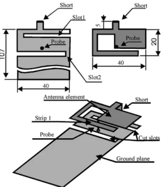
To meet the market demands of device compactness, the subject of antenna miniaturization has been extensively investigated in various literatures. As has been shown in [1-3], some techniques applied to the substrate were utilized for antenna size reduction including the magneto-dielectric composite substrate and the embedded-circuit metasubstrate. However, the cost of the fabrication of these substrates is quite high, so they are not practical for real commercial applications. Electrically small antennas (ESAs), for example small dipole and loop antennas, are easily to be integrated into the circuit, but the external matching circuit is required because of the highly reactive impedance of the ESAs. Although the aforementioned drawbacks can be circumvented by placing a parasitic element near the ESAs to achieve resonance and impedance matching simultaneously in a small area to approach the theoretically lower bound of the quality factor Q [4-5], the bandwidth is still limited by the overall size. Planar inverted-F antennas (PIFAs) are popular because they provide the great degree of design flexibility to achieve multiband and compactness. The PIFA antenna with a spiraling tail or a capacitive loading is capable of dual-band operation with about 50% size of the conventional one [6]. In [7-10], the compact resonant antennas are designed by employing the composite Right/Left-handed transmission line.
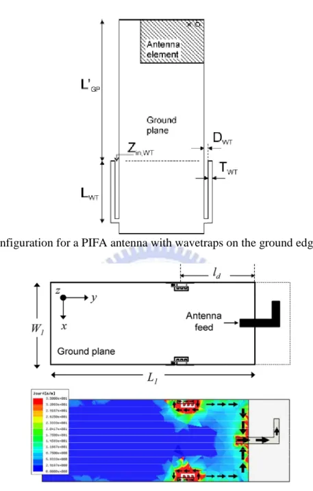
The above-mentioned antenna miniaturization techniques mostly focus on the geometry modification. However, antenna size has fundamental limitations with consideration about gain, bandwidth, and efficiency [11-13]. To achieve better antenna properties, the finite ground plane on the PCB (printed circuit board) has to be considered in the antenna design process. In [14], the performance of the mobile phone for GSM 900/1800 operation was analyzed by the combination of two coupled resonators, the antenna and the chassis (finite length ground plane). The results indicated that the chassis is dominant in contribution of radiation in the lower frequency band. With the increasing knowing of the finite ground plane as a radiator, there are various techniques applied to the ground plane for better antenna performance, such as cutting slots [14-15], using wave traps [16], and adding ground edge current choke (GECC) [17]. In Fig. 1.1, the slots cut on the ground edge is used to extend the current path along the ground edge, which can effectively reduce the resonance frequency of the ground plane for better
3
antenna property in the lower band. Fig. 1.2 shows that the wavetraps are used to electrically reduce the ground size by blocking the ground edge current. The wavetrap is formed by a short circuited quarter-wavelength transmission line. When the wavetraps is in resonance, the impedance looking into the wavetrap is a open circuit. Therefore, the wavetraps can stop the edge current from flowing further and increase the resonance frequency of the ground plane. This is helpful to improve the antenna performance in the higher band. The current choke composed of the printed inductor and capacitor can perform a similar function as wavetraps but with a more compact size. Fig. 1.3 shows the monopole antenna with two chokes on the ground edge. The radiation patterns are improved by limiting the ground edge current with current chokes.
Fig. 1.1. Configuration for a PIFA with cutting slots on the ground edge.
To date, we have known that the ground plane can be used in the antenna design, but the challenge is how to effectively utilize the ground plane for main radiation. Some attempts that utilize the ground plane as the main radiator were published. Coupler-element based antenna designs can excite the chassis resonant mode so that the whole ground plane can radiate effectively [18-19]. Fig. 1.4 shows the configurations of the coupler-based antenna design. To excite the half wavelength resonance mode of the
4
Fig. 1.2. Configuration for a PIFA antenna with wavetraps on the ground edge.
Fig. 1.3. Configuration and simulated current distribution for a monopole antenna with current chokes on the ground edge.
ground plane, the coupler is placed on the ground edge to couple to the ground plane by capacitive coupling. Nevertheless, the position, size and shape of the coupler are restricted for appropriate capacitive coupling. As seen in the figure, the coupler designed in Model 1 is bended to have better performance than the coupler designed in Model 2. However, this will increase the cost due to the fabrication difficulties. Also, these coupler
5
Fig. 1.4. Configuration of two coupler-based antennas
Fig. 1.5. Configuration of a miniaturized slot antenna loaded with bended open end transmission line stub.
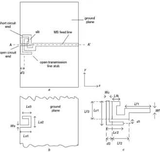
based antennas are still bulky due to the need of additional matching circuit. Traditional microstrip-fed quarter-wavelength slot antennas cut on the ground edge, or their miniaturized versions, are easy to induce radiating edge current. Since the current is highly concentrated along the slot, some current leaking into the ground edge will also contribute partial radiation. Figure 1.5 shows the configuration of a miniaturized slot antenna loaded with bended open end transmission line stub. The capacitive loading is used to cancel the inductive reactance introduced by the reduced slot antenna so that the impedance can be well matched. It must be noticed that the radiation contribution from
6
the slot antenna is lowered with the slot size reduction but the portion of the radiation 5caused by the ground plane increases. However, these slot antennas are still responsible for partial radiation so the size reduction is limited even with the capacitive loading or external matching circuit employed [20-23].
RF/Baseband
Circuitry
_ + Top layer Bottom layer Feed line C1 Ground edge currentFig. 1.6. Configuration of the current driver.
1-3
Contribution
In this thesis, a new microwave component as shown in Fig. 1.6, named current driver, is proposed to activate the ground current flowing along the circuit board edge for radiation. Since the current driver mainly works to transform the input RF signal into the ground edge current and has little responsibility for radiation, the current driver can be designed as small as possible without the necessity to consider much about the degradation of antenna radiation performance. The central idea underlying the design of the current driver is to divide the ground plane into two parts so that the RF signal can be fed in between the parts, without being short circuited, to excite the radiating edge currents. This idea was actually realized in the previous investigations. As shown in [23],
7
the ground plane is physically separated so that the ground plane can be fed as a thick dipole antenna with the external feeding network to achieve impedance matching. However, physically separation of the ground plane is impractical for many applications. In the present study, the ground plane is electrically separated by the proposed compact current driver, which is composed of a very small slot at the edge, a short coupling strip, and a lumped capacitor connected in between the slot. Without the need of the additional matching circuit, the current driver can be matched by appropriately coupling the RF signal to the ground edge through broadside coupling. The equivalent circuit model for the current driver is regarded as a miniaturized planar balun with the differential ports connected to the ground edge [24]. Thus, the ground edge current behaves similar to a dipole antenna fed by the miniaturized balun. Compared with the previously works, the size of the current driver is very small, which is only 3% × 3% of the space wavelength. Moreover, two current drivers can be combined together for dual-band operation. Through the simple design procedures, two resonances with good impedance matching are obtained.
1-4
Thesis organization
This thesis is organized as follows. Chapter II provides the theory of the planar miniaturized marchand balun. In Chapter III, the current driver for single band operation is proposed. The corresponding equivalent circuit model is derived by geometry observation, and the current driver is designed by structure parameter and ground size study. Moreover, the effect of the metal shielding box near the current driver is considered. Another configuration for the current driver with a printed capacitor is also developed. At the end of this chapter, the experiment results and the related discussion are presented. In Chapter IV, the dual-band operation for the current driver is achieved by combining two sing-band current drivers. Thoughtful design procedure for the design of the dual-band current driver is presented. The experiment results are also presented in this chapter. Finally, Section V gives the conclusions.
8
Chapter 2
THEORY OF MARCHAN BALUN
Baluns (balance to unbalance transformer), which can convert the unbalanced signal into the balanced one and also provide impedance transformation, are key components in many applications, such as double balanced mixers, push pull amplifiers, and feeding circuits for balanced antennas. Among them, Marchand balun is the most commonly used balun in microwave circuit, which can be implemented by transmission lines [25] or coupled lines [26-27]. This chapter focuses on the theory of the planar Marchand balun and its miniaturized version with lumped capacitor. Through the analysis of even- and odd-mode half circuit, it shows that the size of Marchand balun can be effectively reduced with the help of a lumped capacitor.
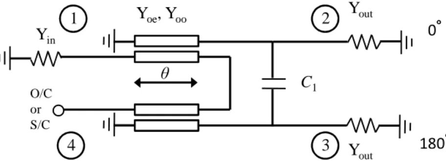
Fig. 2.1 shows the structure of conventional planar Marchand balun, which comprises of two sections of λ/4 coupled lines at the center frequency. However, the size of the conventional Marchand balun makes it impractical for lower band applications. In [24], the balun employs a lumped capacitor in between the balanced outputs can effectively shorten the required coupled line length, which is illustrated in Fig. 2.2.
Unbalanced Input Balanced Outputs Zoe,Zoo Zoe,Zoo O/C λ/4 λ/4
Fig. 2.1. Conventional planar Marchand balun using distributed quarter wavelength coupled lines. C1 Yoe, Yoo O/C or S/C Yin Yout Yout 2 3 4 1 θ 0
°°°°
180°°°°
Fig. 2.2. Miniaturized planar Marchand balun with a lumped capacitor connected in between the balanced output ports 2 and 3.
9 Yout Yout 2 3 0
°°°°
180°°°°
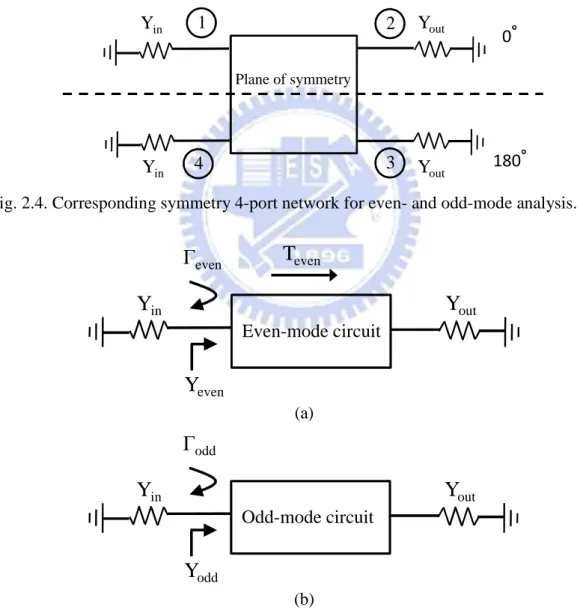
O/C or S/C 4 1 Γ Yin Plane of symmetryFig. 2.3. Schematic diagram for the balun configured as a symmetry 4-port network with one port terminated with an open or short circuit.
Yout Yout 2 3 0
°°°°
180°°°°
4 1 Yin Yin Plane of symmetryFig. 2.4. Corresponding symmetry 4-port network for even- and odd-mode analysis.
Even-mode circuit
T
evenY
inY
outΓ
evenY
even (a) Odd-mode circuitY
inY
outΓ
oddY
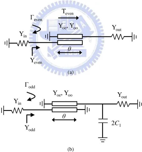
odd (b)Fig. 2.5. (a) Even-mode half circuit circuit. (b) Odd-mode half circuit for the symmetry 4-port network in Fig. 2.4.
10
The miniaturized balun described above can be analyzed through the systematic approach given in [24]. To begin with, the miniaturized Marchand balun is considered as shown in Fig. 2.3, where the symmetry 4-port network with one port terminated with an open or short circuit is depicted. The characteristics of the 3-port balun can be obtained by analyzing the symmetry 4-port network first as illustrated in Fig. 2.4. It is noted that port 4 is terminated with Yin to make the whole structure symmetry. Then, the symmetry
4-port network can be decomposed into even- and odd-mode half circuit for analysis as shown in Fig. 2.5. After some simple computation, the 4-port S-matrix can be derived in terms of the even/odd mode reflection (Γeven and Γodd) and transmission (Teven) coefficient.
Finally, the 3-port S-matrix for the balun is easily derived from the 4-port S-matrix by assigning the boundary condition (Γ) of port 4 as given in Fig. 2.3.
To achieve balun operation, the ports defined in Fig. 2.3 must satisfy the following conditions.
S11=0 (2.1)
21 31
S = −S (2.2)
Apply these conditions into the previously derived 3-port S-matrix. As given in [24], To satisfy (2.1)
even odd even odd even odd + 2 0 2 ( ) Γ Γ − Γ Γ Γ = − Γ Γ + Γ (2.3) To satisfy (2.2) even odd even odd (1 ) 0 2 ( ) T − Γ Γ = − Γ Γ + Γ (2.4)
where the notation Γ denotes the reflection coefficient in port 4 as defined in Fig. 2.3. Assume the denominators in (2.3) and (2.4) are not zero, these equations can be further simplified as follows by replacing Γeven and Γodd by Yeven, Yodd, and Yin defined in Fig. 2.5.
Teven =0 (2.5)
even odd 2 in for the short-circuit case 1
Y +Y = Y Γ = −
11
even odd in
1 1 2
for the open-circuit case = 1
Y +Y =Y Γ
(2.7) Equation (2.5) indicates that, to achieve perfect amplitude and phase, the balun has to present a transmission stop in the even-mode circuit. Moreover, to achieve the input impedance matching, equation (2.6) shows that the sum of the even- and odd-mode admittance must be twice of the source admittance for the short-circuit case. For the open-circuit case, the sum of the even- and odd-mode impedance must be twice of the source impedance as given in (2.7). The equations (2.5)-(2.7) give the valuable insight into the design of the miniaturized balun by analyzing its even- and odd-model half circuits.
Y
oe, Y
ooY
inY
outθ
T
evenΓ
evenY
even (a)Y
oe, Y
ooY
inY
outθ
Γ
oddY
odd2C
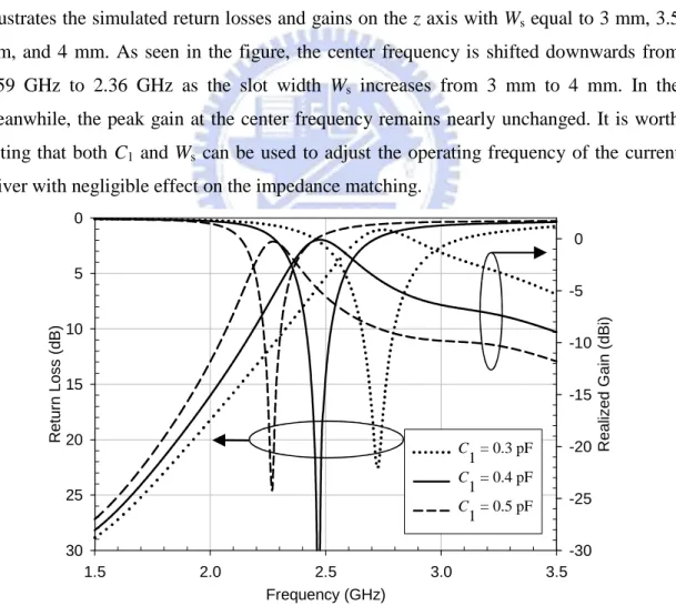
1 (b)Fig. 2.6. (a) Even-mode circuit. (b) Odd-mode circuit for the miniaturized Marchand balun as shown in Fig. 2.2.
12
The miniaturized Marchand balun described in Fig. 2.2 is analyzed by the even- and odd-mode circuit shown in Fig. 2.6. It is recognized that the even-mode circuit in Fig. 2.6 (a) presents a perfect transmission stop (Teven = 0) that is frequency independent for all
values of θ. Thus, equation (2.5) is satisfied automatically. Theoretically perfect and frequency-independent amplitude and phase balance of the miniaturized balun is ensured. To achieve the impedance matching for balun operation, equation (2.6) or (2.7) must be satisfied depending on reflection coefficient Γ of port 4. The even mode and odd mode admittance in Fig. 2.6 can be determined as
even ( ) tan 2 oe oo Y Y Y = j + θ (2.8) 12 21 odd 11 22 ( 2 1 out) Y Y Y Y Y j ωC Y = − + + (2.9) where 11 22 2 tan oo oe Y Y Y Y j θ + = = − 12 21 2 sin oo oe Y Y Y Y j θ − = = −
By substituting (2.8) and (2.9) into (2.6) or (2.7) and equating the real and imaging parts, the equations for Yoe and Yoo can be obtained in the following:
1 in out 1 ( , , , ) oe oe Y F C Y Y Z θ ω = = (2.10) 1 in out 1 ( , , , ) oo oo Y G C Y Y Z θ ω = = (2.11) Where F and G are functions of θ,ωC1,Yin, and Yout.
Based on the design equations for Yoe and Yoo in (2.10) and (2.11), different design
curves can be obtained. The miniaturized balun can be designed by considering the tradeoffs between the coupled line length, capacitance, bandwidth, and impedance transforming ratio, which is more flexible than conventional Marchand balun.
13
Chapter 3
DESIGN OF THE
SINGLE-BAND
CURRENT
DRIVER
3.1
G
EOMETRY ANDC
IRCUITM
ODEL+ F′ _ F A A′ B B′ O O′ C1 h Feed line x y z Ground Top layer Bottom layer M′ (a) Feed line _ Ground + Ls w Ws l2 l1 C1 x y w g l1 (b)
Fig. 3.1. (a) Perspective view of the proposed current driver, where F, A, B, and O points are on the top layer, and F’, A’, B’, O’, and M’ points are on the bottom layer layer. (b) Configuration of the proposed current driver.
14
Unbalanced Input (coaxial line)
Balanced Outputs (connected to ground edge) Zoe,Zoo C1 F F′ A B O A′ B′ Zoe,Zoo O′ lcoup lcoup
Fig. 3.2. Equivalent circuit model for the proposed current driver. TABLE II
Detailed dimensions for the proposed current driver
parameter Ls Ws C1 l1 l2 w g
value 4 mm 3.5 mm 0.4 pF 1.5 mm 2 mm 0.5 mm 1 mm
In this chapter, the proposed current driver is demonstrated at 2.45 GHz for IEEE 802.11 b/g/n WLAN applications. It is fabricated on the ground edge of an FR4 substrate with thickness h = 0.4 mm and dielectric constantεr = 4.4. The size of the substrate is L × W = 50 mm × 100 mm, which is the standard size for PCMCIA applications. Fig. 3.1(a)
and Fig. 3.1(b) show the perspective view and top view of the proposed current driver, respectively. The letters in the figure designate the relative position in the equivalent circuit model shown in Fig. 3.2. The current driver lies in the xy plane and is printed on both sides of the FR4 substrate. It comprises a U-shaped metal strip with strip width of w on the top layer and a slot of size Ls × Ws on the bottom layer. The slot is open to the
ground edge through a small gap g. A lumped-circuit capacitor C1 is connected in
between pointsA′andB′on the bottom layer. This capacitor here can also be replaced by a printed one. The current driver is fed by a 50 Ω feed line, which can be a coaxial line or a microstrip line. The positive terminal of the feed line is connected to one end of the U-shaped strip (point F) on the top layer, and the negative terminal is connected to the ground point near the slot edge (point F′) on the bottom layer. The overall size of the current driver is only 4 mm × 4mm, which is about 0.03λ0 × 0.03λ0, withλ0 being the
15
To explain the operating principle of the current driver, an equivalent circuit model is introduced based on structure observation. It has to be emphasized that this equivalent circuit model is a conceptual model, but not an exact one. In spite of that, the circuit model gives a valuable understanding of the properties of the current driver.
The circuit model is derived as follows: In Fig. 3.1(a), it is noted that the U-shaped metal strip couples to the overlapping slot edge mostly through broadside coupling. Here, a section from points F to A (top layer) and that from F′and A′(bottom layer) are considered as a pair of coupled lines. These two coupling transmission lines share the same ground F′M′O′ along the slot edge on the bottom layer. The reason they form two coupled lines but not a single transmission line will become clear when the simulated surface current distribution on them are depicted later. Similarly, the parallel sections BO (top layer) and B′O′ (bottom layer) form another pair of coupled lines with the same ground F′M′O′. The equivalent circuit model can thus be drawn as Fig. 3.2, which is actually a miniaturized planar balun similar to a conventional planar Marchand balun [26, 27], but with difference in the capacitor C1 between the balanced outputs (points A′and
B′) for size reduction [24]. Because the current driver has a function like a balun, it can generate differential signals at the two ends of the capacitor so the in-phase ground edge currents could be induced. The total radiation is mainly attributed to these induced ground edge currents.
The miniaturized planar balun with a lumped-circuit capacitor shows more degrees of freedom in design than the conventional planar marchand balun does. It can be implemented by a wide range of practical values for even-mode impedance Z0e and
odd-mode impedance Z0o depending on various values of C1 with different lengths of coupled
lines. Moreover, this miniaturized balun structure is theoretically perfect and frequency independent with amplitude and phase balances. Several important characteristics of the miniaturized planar balun that are beneficial to the design of the current driver are listed in the following:
a). The required value of Z0e for the balun increases with decreasing coupled line length
lcoup .
b). The required value of Z0e for the balun decreases when the capacitance C1 increases.
16
C1.
d). For a fixed coupled line length, the balun with larger Z0e and smaller C1 exhibits
wider bandwidth.
From characteristics a) and b), it shows that the balun size can be reduced with large C1
while Z0e is remained fixed. However, characteristic d) indicates the balun with larger Z0e
exhibits wider bandwidth, so C1 and Z0e are appropriately chosen depending on desired
bandwidth.
The proposed current driver is designed similar to the miniaturized balun. The even-mode impedance Z0e of the current driver is determined by the slot width Ws, which is
related to the equivalent distance between coupled lines and ground plane. Thus, Z0e
increases with larger slot width Ws. The coupling strength between the coupled lines is
affected by the strip width w, so odd-mode impedance Z0o is related to the strip width w.
A larger strip width w corresponds to a lower value of the odd-mode impedance. Also, as stated in d), the bandwidth increases when Z0e increases, and thus the larger slot size for
the current driver. Therefore, bandwidth and size are tradeoffs.
3-2
S
INGLE-B
ANDC
URRENTD
RIVERD
ESIGNAs stated, the current driver can be considered as a miniaturized balun, which is characterized by the even-mode impedance Z0e, the odd-mode impedance Z0o, the length
of the coupled lines lcoup, and the capacitor in the circuit model. In this section, the current
driver is investigated through the simulated results of the return losses and total gains on the z axis for these parameters. Without the specification, the other parameters of the simulation are the same as given in TABLE II. The simulation results are obtained using Ansoft High Frequency Structure Simulator (HFSS) [28]. The FR4 substrate loss is considered in the simulation with the loss tangent of 0.02.
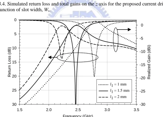
Fig. 3.3 shows the simulated return losses and gains on the z axis for the current driver with various capacitances C1. It is observed that the center frequency is shifted
downwards with increasing C1, from 2.73 GHz to 2.27 GHz as C1 varies from 0.3 pF to
0.5 pF. This trend of the return losses agrees with characteristics a) and b) of the miniaturized balun, which indicate the capacitor C1 is used for size reduction. Good
17
current driver can be easily adjusted by varying C1 with little influence on impedance
matching. Furthermore, the peak gain on the z axis keeps a value near 0 dBi, not changed much due to the variation of C1. The variations of gain over the 10-dB impedance
bandwidth of the current driver for C1 = 0.3 pF, 0.4 pF, and 0.5 pF are 0.66 dBi, 0.5 dBi,
and 0.4 dBi, respectively. This suggests that the ground edge currents induced by the current driver maintain good radiation property despite the change of C1, and thus the
center frequency.
The slot width Ws is a crucial parameter related to the even-mode impedance of the coupled lines in the equivalent model. Characteristic a) of the miniaturized balun shows the required value of Z0e increases with decreasing coupled line length. Thus, the
operating frequency moves downwards when the slot width Ws increases. Fig. 3.4
illustrates the simulated return losses and gains on the z axis with Ws equal to 3 mm, 3.5
mm, and 4 mm. As seen in the figure, the center frequency is shifted downwards from 2.59 GHz to 2.36 GHz as the slot width Ws increases from 3 mm to 4 mm. In the
meanwhile, the peak gain at the center frequency remains nearly unchanged. It is worth noting that both C1 and Ws can be used to adjust the operating frequency of the current
driver with negligible effect on the impedance matching.
Frequency (GHz) 1.5 2.0 2.5 3.0 3.5 R e tu rn L o s s ( d B ) 0 5 10 15 20 25 30 R e a liz e d Ga in ( d B i) -30 -25 -20 -15 -10 -5 0 C 1 = 0.3 pF C 1 = 0.4 pF C 1 = 0.5 pF
Fig. 3.3. Simulated return loss and total gains on the z axis for the proposed current driver as a function of C1.
18 Frequency (GHz) 1.5 2.0 2.5 3.0 3.5 R e tu rn L o s s ( d B ) 0 5 10 15 20 25 30 R e a liz e d G a in ( d B i) -30 -25 -20 -15 -10 -5 0 Ws = 3 mm Ws = 3.5 mm Ws = 4 mm
Fig. 3.4. Simulated return loss and total gains on the z axis for the proposed current driver as a function of slot width, Ws.
Frequency (GHz) 1.5 2.0 2.5 3.0 3.5 R e tu rn L o s s ( d B ) 0 5 10 15 20 25 30 R e a liz e d Ga in ( d B i) -30 -25 -20 -15 -10 -5 0 l1 = 1 mm l1 = 1.5 mm l1 = 2 mm
Fig. 3.5. Simulated return loss and total gains on the z axis for the proposed current driver as a function of l1. It is noted here slot length Ls varies with l1 (Ls = 2l1 + g).
19 Frequency (GHz) 1.5 2.0 2.5 3.0 3.5 R e tu rn L o s s ( d B ) 0 5 10 15 20 25 30 R e a liz e d G a in ( d B i) -30 -25 -20 -15 -10 -5 0 w = 0.3 mm w = 0.5 mm w = 0.8 mm
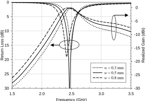
Fig. 3.6. Simulated return loss and total gains on the z axis for the proposed current driver as a function of strip width, w.
In the proposed current driver, the coupled lines are bent into two sections l1 and l2 for
size reduction. The effect of the length of coupled lines is examined by adjusting l1 while
l2 is fixed to 1.5 mm. Fig. 3.5 depicts the return loss and gains on the z axis for various
strip length l1 (1 mm, 1.5 mm, and 2 mm). Obviously, the center frequency moves lower
with larger l1. As l1 increases from 1mm to 2 mm, the center frequency decreases from
2.78 GHz to 2.22 GHz. Notice that the peak gain on the z axis for various l1 is quite stable.
Fig. 3.6 shows the effect on return loss and gains on the z axis for various strip width w (0.3 mm, 0.5 mm, and 0.8 mm). There is a slight frequency shift shown in the figure with varying w. The strip width is related to the coupling coefficient of the coupled lines, especially in l1 section. In addition, the strip width has a dominant effect on Z0o but a
subtle effect on Z0e. Since the required value of Z0o is less sensitive to the coupled line
length (characteristic c). Thus, the change of strip width w would not lead to large frequency shift as expected.
20 Frequency (GHz) 1.5 2.0 2.5 3.0 3.5 R e tu rn L o s s ( d B ) 0 5 10 15 20 25 30 R e a liz e d G a in ( d B i) -30 -25 -20 -15 -10 -5 0 (C1,Ws) = (0.2 pF, 6 mm) (C1,Ws) = (0.4 pF, 3.5 mm)
Fig. 3.7. Simulated return loss and total gains on the z axis for the proposed current driver with two configurations (C1 = 0.2 pF, Ws = 6 mm) and (C1 = 0.4 pF, Ws = 3.5 mm). Other
structure parameters of the current driver (C1 = 0.2 pF, Ws = 6 mm) are Ls = 4 mm, l1=
1.5 mm, l2 = 3 mm, and w = 0.5 mm. Other parameters of the current driver (C1 = 0.4 pF,
Ws = 3.5 mm) are the same as given in TABLE II.
Frequency (GHz) 1.5 2.0 2.5 3.0 3.5 R e tu rn L o s s ( d B ) 0 5 10 15 20 25 30 R e a liz e d G a in ( d B ) -35 -30 -25 -20 -15 -10 -5 0 40 × 50 mm2 50 × 100 mm2 170 × 250 mm2
Fig. 3.8. Simulated return loss and total gains on the z axis for the proposed current driver with ground sizes L × W = 40 × 50 mm2, 50 × 100 mm2, and 170 × 250 mm2. The current driver is placed in the center of the ground edge L.
21
According to characteristic d) of the miniaturized balun, the balun with larger Z0e and
smaller C1 exhibits wider bandwidth. This property is illustrated in Fig. 3.7, which shows
the return loss and gains on the z axis for two sets of C1 and the corresponding slot width
Ws (C1 = 0.4 pF, Ws = 3.5 mm and C1 = 0.2 pF, Ws = 6 mm). The 10-dB return loss
bandwidth changes from 120 MHz (2.40 GHz to 2.52 GHz) to 230 MHz (2.33 GHz to 2.56 GHz) as C1 varies from 0.4 pF (Ws = 3.5 mm) to 0.2 pF (Ws = 6 mm). The cost of
bandwidth enhancement for the current driver is a larger slot size. Thus, the current driver can be designed flexibly for various requirements of bandwidth. In this study, the current driver is designed for 2.45 GHz IEEE 802.11 b/g/n WLAN applications. The bandwidth of the current driver with C1 = 0.4 pF and Ws = 3.5 mm is adequate for the specification.
After the discussion on the effects of the structure parameters and the capacitor C1 on
the current driver, it is necessary to investigate the sensitivity of the antenna performance to ground size. Fig. 3.8 shows that the return loss for various ground sizes, L × W = 40 × 50 mm2, 50 × 100 mm2, and 170 × 250 mm2. It is seen that the ground size has minor effect on the return loss for the current driver. The center frequency is almost unchanged with different ground sizes. The gains on the z axis are also shown in the figure. As observed, the peak gains and gain variations in the 10-dB return-loss bandwidth are about the same. The rapid gain variation in the higher outband for the ground size of 170 × 250 mm2 is due to the high-order-mode current distribution along the edge.
22
3-3
S
HIELDINGB
OXE
FFECT Current driver lbox dy wbox dx Shielding boxx
y
Current driver lbox dy wbox dx Shielding boxx
y
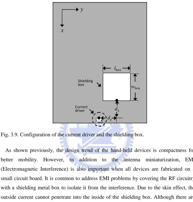
Fig. 3.9. Configuration of the current driver and the shielding box.
As shown previously, the design trend of the hand-held devices is compactness for better mobility. However, in addition to the antenna miniaturization, EMI (Electromagnetic Interference) is also important when all devices are fabricated on a small circuit board. It is common to address EMI problems by covering the RF circuitry with a shielding metal box to isolate it from the interference. Due to the skin effect, the outside current cannot penetrate into the inside of the shielding box. Although there are openings on the shielding box for the signals to come in and out, the shielding box can still functions well because the size of the openings is very small compared to the wavelength of the operating frequency. In this section, we will simulate the effect of the shielding box on the current driver as a function of the position and size of the shielding box. The simulation is conducted by ANSOFT HFSS. Finally, the result of the current driver with the shielding box is compared with the previous result without the shielding box, and the shielding box effect can be easily addressed by adjusting the structure parameter slot width WS.
23 Frequency (GHz) 1.5 2.0 2.5 3.0 3.5 R e tu rn L o s s ( d B ) 0 5 10 15 20 25 30 dx=3mm,dy=0mm dx=1mm,dy=0mm dx=0mm,dy=0mm dx=0mm,dy=15mm (a) -35 -25 -15 -5 5 0 30 60 90 120 150 180 210 240 270 300 330
x
z
dx= 0mm,dy= 0mm (2.63 GHz) dx= 1mm,dy= 0mm (2.53 GHz) dx= 3mm,dy= 0mm (2.48 GHz) dx= 0mm,dy= 15mm (2.47 GHz) (b)Fig. 3.10. (a) Simulated return loss for the proposed current driver with the shielding box of different positions. (b) Simulated total radiation field patterns in xz plane for the current driver with shielding box of different positions. The size of the shielding box is 20 × 20 × 2 mm3. The parameters of the current driver are the same as given in TABLE II.
24
The effect of the shielding box on the current driver is investigated. As shown in Fig. 3.9, the shielding box is placed on the top layer with surrounding shorting poins connected to the ground plane through the substrate. The geometrical parameters of the shielding box are length lbox, width wbox, and height hbox (+z direction). The distance
between the shielding box and the current driver is decomposed into two components, vertical component dx and horizontal component dy. Fig. 3.10 helps to understand the
effect of the shielding box on the return loss and gains of the current driver when the shielding box is placed at different positions. The size of the shielding box is lbox × wbox ×
hbox = 20 × 20 × 2 mm3. As seen in Fig. 3.10(a), the frequency responses of the return
loss have similar behaviors for dx = 3, 1, and 0 mm (with dy fixed at 0 mm). The center
frequency is slightly shifted from 2.48 to 2.63 GHz. The more the shielding box is moved toward the current driver, the higher is the center frequency. Only 6% frequency shift is observed even when the shielding box is put directly above the current driver (i.e., dx = dy
= 0 mm). As will be seen later, this slight frequency shift can be easily restored by tuning the driver’s structure parameter. Although not shown here, the shielding box has negligible effect on the current driver when the vertical distance is more than 3 mm. Also, since the induced current is concentrated on the ground edge for radiation, the effect of the shielding box placed along the edge is also considered. The fourth curve in Fig. 3.10(a), dx = 0 mm and dy = 15 mm, represents the return loss when the shielding box is
aligned with the right side of the ground edge. The response is almost identical to that of a stand-alone current driver, which means that the proximity shielding box has no obvious effect on the current driver.
Fig. 3.10(b) shows the simulated total radiation field patterns in xz plane for the current driver with the shielding box at different positions. The radiation patterns are omni-directional and almost the same with average gains varying between 0.65 dBi and 1.04 dBi. This implies that the existence of the nearby shielding box has little influence both on the return loss response and the radiation performance of the current driver.
25 Frequency (GHz) 1.5 2.0 2.5 3.0 3.5 R e tu rn L o ss (d B ) 0 5 10 15 20 25 30 20 × 20 × 2 mm3 20 × 20 × 4 mm3 40 × 40 × 2 mm3
Fig. 3.11. Simulated return loss for the proposed current driver with shielding box of different sizes. The shielding box is aligned with the slot edge of the current driver (dx =
0 mm and dy = 0 mm). The parameters of the current driver are the same as given in
TABLE II. Frequency (GHz) 1.5 2.0 2.5 3.0 3.5 R e tu rn L o s s (d B ) 0 5 10 15 20 25 30
without shielding box, Ws = 3.5 mm with shielding box, Ws = 3.5 mm with shielding box, Ws = 4.2 mm
Fig. 3.12. Simulated return loss for the proposed current driver with and without the presence of the shielding box. The shielding box is placed directly above the current driver (dx = 0 mm and dy = 0 mm) with the size of 20 × 20 × 2 mm3. The parameters of
26
The influence of the shielding box volume is examined in Fig. 3.11, which shows the return loss of the current driver for various sizes of the shielding box. It can be seen that the return loss is nearly not affected by the width and height of the shielding box. The return loss curve for the 20 mm × 20 mm × 2 mm shielding box is almost overlapped with the curve for the 40 mm × 40 mm × 2mm one. Furthermore, by comparing the first curve (20 mm × 20 mm × 2 mm) and the second curve (20 mm × 20 mm × 4 mm), the center frequency moves from 2.63 GHz to 2.65 GHz as hbox varies from 2 mm to 4 mm.
This variation shows that the height of the shielding box has minor effect on the return loss.
From the above discussion, the vertical distance dx of the shielding box is the most
important factor that determines the amount of frequency shift. However, even in the worst cast that the shielding box is placed directly above the current driver (i.e., dx = dy =
0 mm), the frequency shift can be easily resumed by slightly adjusting the current driver’s dimension. To demonstrate this, Fig. 3.12 shows the simulated return loss with and without the presence of a shielding box. The dotted line indicates the frequency response of the original design (with slot size of Ls × Ws = 4 × 3.5 mm2) without the
proximity shielding box, which shows a design frequency at 2.47 GHz. After putting the shielding box of size 20 mm × 20 mm × 2 mm directly above the current driver (dx = dy =
0 mm), the response turns out to be the dashed line, where the center frequency is now shifted to 2.63 GHz. To tune the frequency into the design one, we simply increase the slot width Ws of the current driver from 3.5 mm to 4.2 mm. The increase of the slot width
would decrease the center frequency (as shown in Fig. 3.4), so that the resultant frequency response (solid line) resumes to the design one.
27
3-4
S
INGLE-B
ANDC
URRENTD
RIVERD
ESIGN WITH AP
RINTEDC
APACITORFeed line
Ground
L
sW
sl
x
y
+
w
w
cg
g
e_
Fig. 3.13. Configuration of the proposed current driver with a printed interdigital capacitor.
TABLE III
Detailed dimensions for the proposed current driver with a printed capacitor parameter Ls Ws N1 l w g = ge wc
value 4 mm 4 mm 10 2 mm 0.5 mm 0.2 mm 0.2 mm As demonstrated previously, the center frequency of the current driver is very sensitive to the capacitance. However, the lumped capacitor inevitably has the fabrication inaccuracy. This may cause problem, especially for narrow band applications. Also, using lumped capacitor in the design will increase the fabrication cost. To reduce the cost and increase the design flexibilities, the current driver for 2.4 GHz WLAN applications is redesigned with another configuration by replacing the lumped capacitor with the printed one as shown in Fig. 3.13. In the figure, the current driver lies in the xy plane and is printed on both sides of the FR4 substrate. It comprises a U-shaped metal strip with strip width of w on the top layer and a slot of size Ls × Ws on the bottom layer. Inside the slot
28
are filled with a printed interdigital capacitor. The interdigital capacitor is defined by the figure width wc, the gap between figures g, the gap at the end of the fingers ge, and figure
number N. The finger length varies with the slot length Ls. Also, the U-shaped metal strip
is aligned with slot edge, and has two arms of the length l. The whole size of the current driver is determined by the slot size Ls × Ws. The current driver is fed by a 50 Ω
transmission line, which can be a coaxial line or a microstrip line with the positive terminal connected to one arm of the U-shaped metal strip and the negative terminal connected to the ground plane near the slot edge. The driver, which is located in the center of the shorter ground edge, is fabricated on an FR4 substrate of 50 mm × 100 mm with thickness h = 0.4 mm and dielectric constant εr = 4.4.
The design of the current driver with a printed capacitor is basically the same as those described above for the current driver with a lumped capacitor. The center frequency is determined by the slot size Ls × Ws and the capacitance. Moreover, the input impedance is
easy to be matched at 50 Ω with appropriate coupling strength, which is controlled by the strip width w and arm length l1 of the U-shaped metal strip on the top layer. Detailed
dimensions for the current driver are listed in TABLE III. It is noticed that the overall size for the current driver with a printed capacitor remains the same as the size for the current driver with lumped capacitor.
The performance of the two configurations for the current driver is compared in Fig. 3.14, which shows the frequency response of the return loss for the current driver with the printed capacitor and lumped capacitor. It is observed in the figure that the two curves are almost overlapped with each other at 2.45 GHz. This reveals that the overall performance of the current driver is not changed with the lumped capacitor replaced with a printed one. However, the printed capacitor is easy to generate unwanted resonance in the higher frequency, which is not able to induce radiating ground edge for radiation. The additional return loss deep at 5.9 GHz is observed in the figure, which is purely generated by the structure of current driver itself and is basically irrelevant to the ground edge current. Thus, the radiation property is very poor. Although not shown here, the simulated total radiation efficiency is only about 10 %.
29 Frequency (GHz) 1.5 2.0 2.5 3.0 3.5 4.0 4.5 5.0 5.5 6.0 R e tu rn L o s s (d B ) 0 5 10 15 20 25 30 Printed Capacitor Lumped Capacitor
Fig. 3.14. Simulated return loss for the current driver with a printed interdigital capacitor and the lumped capacitor. The parameters for the two current drivers are given in TABLE II and III, respectively.
30
3-5
M
EASUREMENTA
NDD
ISCUSSION3-5-1
Current driver with a lumped capacitor
Frequency (GHz) 1.5 2.0 2.5 3.0 3.5 R e tu rn L o s s ( d B ) 0 5 10 15 20 25 30 R a d ia ti o n E ff ic ie n c y ( % ) 0 20 40 60 80 100 Measurement Simulation
Fig. 3.15. Simulated return loss and radiation efficiency as well as measured return loss for the proposed current driver with a lumped capacitor. The simulated radiation efficiency includes the mismatch loss. The parameters for the current driver are the same as given in TABLE II.
In this section, the measurement results and the corresponding discussion for the proposed current driver fabricated on the ground plane of 50 × 100 mm2 are presented. Fig. 3.15 shows the simulated return loss and radiation efficiency as well as the measured return loss for the proposed current driver with a lumped capacitor. As seen in the figure, the simulated and measured results come to a great agreement. The measured return loss shows 120 MHz 10-dB return-loss bandwidth centered at 2.46 GHz. In addition, over the bandwidth for IEEE 2.4 GHz WLAN operation, the radiation efficiency varies slowly from 74% to 86%.
31 -35 -25 -15 -5 5 0 30 60 90 120 150 180 210 240 270 300 330
x
y
x
y
E
φE
θE
total (a) -35 -25 -15 -5 5 0 30 60 90 120 150 180 210 240 270 300 330x
z
-35 -25 -15 -5 5 0 30 60 90 120 150 180 210 240 270 300 330z
y
(b) (c)Fig. 3.16. Measured 2-D radiation patterns for the proposed current driver with a lumped capacitor at 2.45 GHz. The driver is fabricated on the ground plane of 50 mm by 100 mm. (a) xy plane. (b) xz plane. (c) yz plane.
TABLEIV
MEASURED GAINS AT 2.45GHZ FOR THE CURRENT DRIVER WITH A LUMPED CAPACITOR 2.45 GHz xy plane xz plane yz plane
Peak gain (dBi) 0.44 1.20 -0.36
32 Frequency (GHz) 2.35 2.40 2.45 2.50 2.55 0 20 40 60 80 100
Fig. 3.17. Measured radiation efficiency for the current driver with a lumped capacitor. The measured radiation patterns at 2.45 GHz in the three principal planes are illustrated in Fig. 3.16. There are generally no nulls for the total-power radiation patterns Etotal observed in the three principal planes. This omni-directional property makes the
proposed current driver promising for many applications. The corresponding values of measured peak and average gains in three principal planes are listed in TABLE IV. About 0 dBi average gain is obtained in the nearly omin-directional pattern in xz plane. Also, the measured antenna radiation efficiency is given in Fig. 3.17, where the efficiency varies from 62% to 74% over the band for 2.4 GHz WLAN application. It is noticed that about 10% efficiency difference between the simulated and measured results is observed. This is because that the ohmic loss caused by the cable and the lumped capacitor is not considered in the simulation. The radiation properties of the current driver are quite good, as compared to general printed antennas fabricated on the same substrate.