國 立 交 通 大 學
顯示科技研究所
碩 士 論 文
無轉態液晶反應單體修飾光學補償彎曲液晶盒之
研究
The study of Transition free Liquid Crystal Reactive
Monomer Modified OCB Cell
研 究 生 : 周蓮馨
指 導 教 授 : 陳皇銘
中 華 民 國 九 十 七 年 六 月
無轉態液晶反應單體修飾光學補償彎曲液晶盒之研究
The study of Transition free Liquid Crystal Reactive Monomer
Modified OCB Cell
研 究 生 : 周蓮馨
Student : Liansing Chow
指 導 教 授 : 陳 皇 銘
Advisor : Huang-Ming Philip Chen
國 立 交 通 大 學
電 機 學 院
顯 示 科 技 研 究 所
碩 士 論 文
A Thesis
Submitted to Display Institute College of Electrical Engineering
National Chiao Tung University in Partial Fulfillment of the Requirements
for the Degree of Master
In
Display Institute June 2008
Hsinchu, Taiwan, Republic of China.
i
無轉態液晶反應單體修飾光學補償彎曲液晶盒之研究
研究生: 周蓮馨 指導教授: 陳皇銘 博士
國立交通大學顯示科技所
摘要
在新興的 21 世紀,巨大的超級電腦已經被嬌小的筆記型電腦,或者是超薄型電腦 取而代之,以往的大型 CRT 螢幕已經轉為超薄或是大型的液晶螢幕取代。液晶螢幕因 為內部液晶的特殊電場反應,因而廣為社會大眾所使用,此外,液晶非常輕、薄、短、 小,更有許許多多不同種類的液晶相繼問世,也形成大家爭相研究的對象之一。但液晶 仍具有許多需要改良的地方,舉凡反應時間、以及動態影像品質,仍有很大的進步空間。 而在這許多的液晶模式當中,光學補償彎曲液晶盒,也就是所謂的 Pi cell 或是 OCB cell, 更為許多團體主要的研究對象。(optically compensated bend ,OCB 或稱 Pi-cell)。光學補償彎曲液晶盒(OCB cell),主要有三種狀態,首先在無電壓狀態下,其為 Splay 狀態,當加上一電壓大於臨界電壓則有 bend 狀態產生,這也是光學補償彎曲液晶盒主 要操作範圍的起始點,同時也是亮態,當電壓加到很大時,則有液晶全部站直的狀態產 生,同時也是主要的暗態,其特性為反應時間快,缺點為需提供一偏壓大於臨界電壓, 方可啟動液晶,並達到可用的亮態區域。 本篇論文主要探討,如何使用新材料與原本的光學補償彎曲液晶盒配合,使得液晶 得以不需加上一偏壓,在起始狀態即為亮態,並且維持原本的高對比度等優點。
ii
The study of Transition free Liquid Crystal Reactive Monomer
Modified OCB Cell
Student: Liansing Chow Advisor: Dr. Huang-Ming Philip Chen
Display Institute
National Chiao Tung University
Abstract
In the newly 21th century, the giant super computer in the 20th century has been replaced by small and tiny notebooks or super thin computers. The CRT screen has been replaced by liquid crystal screen with a characteristic that very thin, very small, very light, and moreover, very short. The liquid crystal screen has a distinguishing feature that it responses to the electric field with different reactions. Accompany with different kind of liquid crystals be presented to the public, and some deficiencies with different kind of liquid crystal, like response time and the quality of the moving images, it becomes a new target to the researchers.
Among those different kinds of liquid crystals, optically compensated bend, also known as OCB cell or Pi cell, has a characteristic that its response time is fast and has high contrast ratio. OCB cell was operated at bend and vertical state, and also known has a big deficiency that it needs a voltage bigger than the critical voltage to have the splay state become the bend state, also called as transition.
In this thesis, we will discuss how to use a new material to operate with the original OCB cell and form the OCB cell in a condition without transition and still has the advantages of the original OCB cell.
iii
誌謝
在這兩年的研究生活中,曾受到許多人的幫助,首要感謝的就是我的指導教授 陳 皇銘老師以及師母,在我徬徨及需要意見的時候,適時給我客觀的建議及分析,幫助我 做出適當的決定。在研究上,引導我深入液晶顯示領域,對於我的研究有莫大的幫助。 其次,感謝實驗室學長姐們-威慶、佳恬、昆展、鴻杰、耿睿、文孚、佑儒、俊民、 彣綺、世民、宜揚的細心教導及建議,讓我慢慢進入狀況,知道做研究應該是怎麼回事, 總是在生活上、研究中給我適當的幫助,以及同學們-怡帆、謹瑋、祥志,以及學妹-毓筠和其他的學弟妹,總是在你們忙的時候,抽空幫我分擔一些工作,幫助我的實驗可 以順利完成。 最後,要向我的家人表達出我的感謝,謝謝你們一直默默的支持我,讓我順利的完 成碩士的學業。iv
Table of contents
Abstract in Chinese i Abstract in English ii Acknowledgement iii Table of contents iv List of Tables viList of Figures vii
Chapter 1 INTRODUCTION AND BACKGROUND 1
1-1 INTRODUCTION OF LIQUID CRYSTALS 1
1-2 LIQUID CRYSTALS 1
1-2-1 Liquid crystal Phase 2
1-2-2 Phase 1-Nematic 3 1-2-3 Phase 2-Smectic 4 1-2-4 1-2-5 1-2-6 1-2-6-1 1-2-6-2 Phase 3-Cholesteric Phase versus temperature Liquid crystal optics
Light basic properties
Light wave‘s propagation in Nematic liquid crystal
4 5 6 6 8
1-3 SOME CHARACTERS AND STRUCTURE OF LCD 10
1-4 LCD OPERATION 10
1-5 OPTICAL COMPENSATED BEND (OCB) MODE OF LC 11
1-6 MOTIVATION AND OBJECTIVE 11
1-7 ORGANIZATION OF THIS THESIS 12
Chapter 2 OVERVIEW OF OCB CELL 13
2-1 THE CHARACTERISTICS OF OCB CELL 14
2-1-1 The structure of OCB cell 14
2-1-2 Fast response 16
2-1-3 2-1-4
Wide viewing angle
Nucleation and phase transition
16 18
2-1-5 Light leakage in dark state 20
v
Chapter 3 MEASUREMENT SYSTEMS 22
3-1 ATOMIC FORCE MICROSCOPE 22
3-2 CELL GAP MEASUREMENT SYSTEM 25
3-3 LASER OPTICS SYSTEMS 29
3-4 POLARIZED OPTICAL MICROSCOPE 31
Chapter 4 EXPERIMENTS AND RESULTS 33
4-1 CELL FABRICATION PROCESS 34
4-2 CHARACTERISTICS OF REACTIVE NEMATIC LC MONOMERS 38
4-3 NOVEL OCB-CELL MODEL 39
4-4 MEASUREMENT OF ELECTRO-OPTICAL PROPERTIES AND
RESULTS 41
4-4-1 Phase transition free OCB cell 41
4-4-2 Retardations 44
4-4-3 RMM surface tilt angle 45
4-4-4 Contrast ratio 46 4-5 SUMMARIES 49 Chapter 5 CONCLUSIONS 50 5-1 SUMMARY 50 5-2 FUTURE WORKS 51 References 52
vi
List of Tables
Table 4-A Parameters of spin coating polyimide……….... 35
Table 4-B Rubbing Conditions for Polyimide glasses……….... 35
Table 4-C Parameters for RMM-19B……….…. 36
Table 4-D The parameters of liquid crystal ZCE-5096XX…...………... 37
Table 4-E RMM thickness with spin coating speed‘s relation……….... 40
Table 4-F 4wt% RMM-OCB cells and conventional OCB cell-1………..… 42
Table 4-G 4wt% RMM-OCB cells and conventional OCB cell-2………..… 42
Table 4-H The transmittance of RMM2-OCB cell when in different include θ…..… 44
Table 4-I FLC-RMM cell, △n of RM when θ=0……… 46
Table 4-J △n of RMM-OCB cell and pretilt angle………. 46
Table 4-K(a) Contrast ratio of RMM-OCB cells and conventional OCB cell-1………. 47
vii
List of Figures
Fig 1-A Types of rod-liked liquid crystals, (a) Nematic, (b) Smectic (A type), and
(c) cholesteric liquid crystal...………. 2
Fig 1-B The main axis of Nematic liquid crystal………. 3
Fig 1-C Smectic has layer structure because of the two orientations…….………. 4
Fig 1-D Cholesteric liquid crystals‘ helical structure, it can reflect the incident
light…. ……….………..…… 5
Fig 2-A OCB cell‘s structure and five configurations…..………... 14 Fig 2-B Schematic figure of the dynamics in the pi-cell. The flow induces the
torque to accelerate to relax………..……….. 15
Fig 2-C (a) Splay state, (b) Voff (Vcr), bend mode, and OCB cell is in the bright
state. (c)Von, homeotropic state, and OCB cell is in the dark state……… 16
Fig 2-D Experimental results of the viewing-angle-dependent transmittance for
TN cell and OCB cell………. 17
Fig 2-E Cross-section view of OCB cell, it has symmetric viewing angle……... 17
Fig 2-F Mechanism of bend transition……… 18
Fig 2-G The pretilt angle versus energy distribution of splay state and bend state. 19
Fig 2-H Gibbs‘s free energy of bend and splay states as a function of applying
voltage……… 19
Fig 2-I The LC molecules alignment of (a) VA mode, and (b) dark state of OCB
cell………... 21
Fig 3-A (a) Block Diagram of Atomic Force Microscope (b) Concept of AFM
and the optical lever……… 23
Fig 3-B UV/Vis spectrometer LAMBDA 950 from Perkin Elmer……….. 26
Fig 3-C Two surfaces possess reflective index R1 and R2, light would pass
through surface 1 and 2 and causing a light interference…….………….. 27
Fig 3-D The spectrum result for the sample as an example…...……….. 28
Fig 3-E The scheme of laser optic system………... 29
Fig 3-F (a) the installation of retardation measurement(b) LC cell position…….. 30
Fig 3-G The picture of POM……… 31
Fig 4-A Fabrication process of OCB cells..………. 34
Fig 4-B The two different types: (a) only the bottom substrate uses RMM layer
glasses. (b) Both substrate use RMM layer on it……… 37
Fig 4-C The scheme of RMM-OCB cell under (a) 0V, (b) 6V……….……... 39
Fig 4-D RMM-19B microscopic structure observed by AFM. RMM-19B forms a
thin film about 100~200 nm with 3 nm roughness………. 40
viii
Fig 4-F The relation between the RMM layer‘s thickness and the cell‘s Critical
voltage corresponds to different spacers………. 41
Fig 4-G The include angle θ=45° between RMM-OCB cell‘s rubbing direction
and polarizer‘s direction………. 42
Fig 4-H Different thickness of RMM layers with (a) cell gap around 5um, and
(b) cell gap around 3um, and (c) RMM layer on both substrates………... 43
Fig 4-I (a) is conventional OCB cell‘s retardation (b) on the right is retardations
of the RMM-OCB cells under applied voltage from 0V to 6V with
different viewing angle……….……….………. 44
Fig 4-J (a) RMM-OCB cell under7V (b) conventional OCB cell under 7V…... 48
Fig 4-K (a) RMM-OCB cell under0V (b) conventional OCB cell under 2V…….. 48
Fig 4-L (a) Contrast state of RMM-OCB cell (b) contrast state of conventional
1
-CHAPTER 1
INTRODUCTION AND BACKGROUND
1-1 INTRODUCTION OF LIQUID CRYSTALS
Liquid crystalline phase is first discovered by Dr. F. Reinizer [1] in 1888 and the well known term ―liquid crystal‖ is introduced by Lehmann [2] in 1890. Liquid crystals are substances that exhibit a phase of matter that has properties between those of an isotropic liquid, and those of a solid crystal.
In these years, Internet and digital information market grow up fast beyond imagination. Because LC display has many advantages, such as thin, light weight, low power consumption, no radiation pollution, and the most important, compatible with semi-conductor technology, the application of LC display has grown up fast, too. The technology includes material, equipment, manufacture, and product character‘s development. Until today, the LC displays are still growing up with amazing speed, and become the lead of planar display market.
1-2 LIQUID CRYSTALS
In 1888, Austrian botanical physiologist Friedrich Reinitzer found that cholesteryl benzoate does not melt like other compounds, but had two melting points. At 145.5°C it melted into a cloudy liquid, and at 178.5°C it melted again and the cloudy liquid became clear. Next year, Otto Lehmann, a physicist from Karlsruhe, Germany, found out the birefringence
2
-character of liquid crystal, the optical anisotropic. In 1890, these two people called the new phase of matter liquid crystal as fourth state of matter or meso-phases.
1-2-1 LIQUID CRYSTAL PHASE
Liquid crystal phase is a state between solid state and liquid state, also called the forth state. As a result, it has both the solid character and liquid characters. The structure is similar to crystal‘s arrangement, and the liquid character can help the molecule change the position and point direction.
The structures of LC molecules are asymmetric, can be classified into two major shapes, rod-liked and disk-liked. Rod-liked molecules tend to orient themselves around the rubbing direction of the substrate, and align parallel to each other to a preferred direction which is so called self-assembly. To be more accurate, Rod-liked liquid crystal material can be divided into three major types of liquid crystals—Nematic, Smectic, and Cholesteric.(Fig.1-A)
Liquid crystals have another important character, uni-axial anisotropy. This character can let Liquid crystals have different refractive index, magnetic susceptibility, dielectric constant in different orientation.
(a) (b) (c)
Fig. 1-A: Types of rod-liked liquid crystals, (a) Nematic, (b) Smectic (A type), and (c)
3
-1-2-2 PHASE 1- NEMATIC
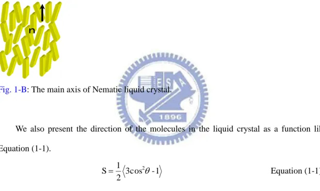
Nematic is a kind of liquid crystal that most like the liquid. Nematic has small viscosity and fast response time. It‘s the earliest liquid crystals that been used in LC TV, monitor, and all types of display elements [3, 4, 5]. It has the worst alignment compare to other liquid crystal. Nematic has a main axis that all molecules would roughly point toward the direction, like the ―n‖ direction in (Fig. 1-B). We can define the direction ―n” as a vector.
Fig. 1-B: The main axis of Nematic liquid crystal.
We also present the direction of the molecules in the liquid crystal as a function like Equation (1-1). 1 -3cos 2 1 S 2 Equation (1-1) ―S‖ is the order parameter, θ is the angle between molecule‘s long axis and n. ―S” would be ―0‖when in isotropic state, and ―1‖ when in a solid state. As a result, when molecules aligned perfectly parallel, θ=0, and S will be ―1‖, the light will pass and the liquid crystal would be transparent. When molecules aligned randomly, θ=random, S will be ―0‖, the light can‘t pass. Generally, liquid crystal molecules have 0.5<S<0.7.
4
-1-2-3 PHASE 2- SMECTIC
On the contrary, Smectic is a kind of liquid crystal that most like the solid. Smectic has high viscosity and slow response time, so their main application is optical data storage materials, they are rarely been used in displays.
Smectic has two orientation of alignment, so they can align like layers (Fig. 1-C). It has different aligned directions in different layers, but the molecules in the same layer would tend to have the same aligned direction. Smectic can be classified into A to L 12 different kinds and named in the order by the time they were found. For example, Smectic A phase, Smectic C phase. In Smectic A phase, the molecules align perpendicular to the layer planes, and in Smectic C phase the alignment of the molecules is at some arbitrary angle to the normal.
Fig. 1-C: Smectic has layer structure because of the two orientations.
1-2-4 PHASE 3- CHOLESTERIC
Cholesteric liquid crystal, also called ―Chiral Nematic liquid crystal‖, is stacked by many layers of Nematic liquid crystals, and aligned in helical planes that parallel with each other. Each surface has different long axis, the adjacent long axes have an included angle.
When the two adjacent long axes have the same orientation, the distance between the two planes calls a pitch (Fig. 1-D). The pitch will change with different temperature, pressure, electric field, or magnetic field. Besides, Cholesteric has optical rotation, it can reflect the
5
-incident light with 2πn (n is average refractive index). Therefore, when the temperature changed, it will have a selective reflection because of different wavelengths and causes a color variation. As a result, it can be used as a temperature sensor. Besides, the alignment of molecules are easily been affected by the electric field, it also can be used as reflective displays, and electronic paper [6].
Fig. 1-D: Cholesteric liquid crystals‘ helical structure, it can reflect the incident light.
1-2-5 PHASES VERSUS TEMPERATURE
The different alignment of liquid crystals accompany with the change of temperature can be expressed as follows:
Solid Smectic Nematic Isotropic Crystal Liquid Crystal Liquid Low temperature High temperature
The alignment of molecules will become isotropic and liquid when the temperature is higher than the clearing point, also called TN-1. At this point, liquid crystal will become clear
and transparent.
6
-1-2-6 LIQUID CRYSTAL OPTICS
When light passes through liquid crystals, it can have some effect like refraction, interference, diffraction, and polarization. Light is a kind of electromagnetic wave and has also can be divided into different kinds and colors by different wavelength. As a result, we will discuss only the monochromatic plane light wave in the following.
1-2-6-1 Light basic properties
From Maxwell equations, we can derive wave equations:
t J -t P -t E c 1 ) E ( 2 0 2 0 2 2 2 Equation (1-2)
For a generalized three dimensional monochromatic plane light wave, it propagate in a uniform dielectric substance, then
P
0
E
, andJ0.0 t E c n ) E ( 2 2 2 2 Equation (1-3)
The refraction index could be: n
n c v
From Equation (1-3), we can get wave function as: ] r k -t cos[ A t) , r ( E Equation (1-4)
Because light is a transverse wave, the polarization direction is the direction of the electric field. We define the travel direction as z direction, so the electric field of monochromatic plane light wave will vibrate in x-y plane.
Then we can rewrite Equation (1-4) as two vectors perpendicular with each other.
) kz -t cos( A Ex x x ) kz -t cos( A Ey y y Equation (1-5)
7
-describe the polarization of light wave simply, take z=0 to see the change of the vibration verses time on the x-y plane, then Equation (1-5):
) t cos( A Ex x x ) t cos( A Ey y y Equation (1-6)
We can define the phase as: y-x。If δ= 0 or π,then
x x y y E A A E , or x x y y E A A -E Equation (1-7)
From Equation (1-7), when the electric field vibrates in
x y
E E
direction, we call it as linear polarization state. We use a new math calculate way to describe the polarization state of light--- Normalized Jones Vector:
i yx y i x 2 y 2 x A e e A A A 1 J Equation (1-8)
When the light wave is linear polarized (δ= 0 or π), the x axis has an included angle of Ψ, then: sin cos J Equation (1-9) And 0 J J 2 Equation (1-10)
So the two factors are orthogonal with each other. When Ψ=0:
0 1 Jx , and 1 0 Jy Equation (1-11)
8
-1-2-6-2 Light wave’s propagation in Nematic liquid crystal
When we consider Nematic liquid crystal cells as uni-axial and anisotropic medium, we can have the light effects as follows:
In uni-axial medium, we have three refraction indexes as nx, ny, nz.
We have: (1) nx=ny=no, calls ordinary index. (2) nz=ne, calls extraordinary index.
When ne>no, the medium were named as positive uni-axial medium. When ne<no, the medium
would be negative uni-axial medium.
We can get two modes from light propagate in uni-axial medium, ordinary wave and extraordinary wave.
We can present the two refractive indexes as:
O wave: n =no Equation (1-12) E wave: 2 e 2 2 o 2 2 e n sin n cos ) ( n 1 Equation (1-13)
θ is the included angle of the propagate direction and z axis(light axis).
As a result, when light propagate in this medium, the two directions of propagations will have different propagate and phase velocities, and also phase retardations. Before the light passes through the medium, the two parts of light will combine together again.
Here are two examples:
I. When the direction of propagation along z axis(light axis):
Then θ will become 0, and substitute into Equation (1-12) and Equation (1-13). We will get:
O wave:n =no and E wave:n (0) =no
Since the two has the same phase velocity, )s
c ( n k
k1 2 o . After light propagate in this two modes for a distance d, from Equation (1-4), the light does not have phase retardation.
9
-That means the polarization of light won‘t change.
II. When the direction of propagation along x-z plane:
From Equation (1-12) and Equation (1-13):
O wave:n =no and E wave:
2 -1 2 e 2 2 o 2 e n sin n cos ) ( n
O wave has wave vector: )s
c ( n
ko o ,
E wave has wave vector : )s
c )( ( n
ke e ,
We can derive the phase transition for Equation (1-8), the light propagate in this medium for a distance d,
O wave has a phase transition: )d
c (
no ,
E wave has a phase transition: )d
c )( (
ne , the two has a phase retardation Γ:
)d c ]( n -) ( [ne o Equation (1-14) Or ]d n -) ( [n 2 o e Equation (1-15)
This phase retardation can generate a change of light polarization, from Equation (1-8). Light propagate in the liquid crystals will change the phase because of the phase retardation and causes different light intensity passes through. By controlling the liquid crystals to change the light intensity is also the main function uses in liquid crystal display.
(The derivation and formulas from Equation (1-2) to Equation (1-15) are come from the book ―Elements of Photonics, Volume I: In Free Space and Special Media.‖ [7])
10
-1-3 SOME CHARACTERS AND STRUCTURE OF LCD
LCD is a kind of displays that uses liquid crystal to control the polarization of polarized light waves and form a display element. LC cell can make the light travel in a fixed direction. Since liquid crystals cannot emit light by itself, it needs a backlight. In the present market conditions, we often use CCFL and LED as the backlight. But they are not planar light, so they need ELP and diffuser to turn the point light or linear light into uniform planar light.
We also need polarizer and analyzer to polarize and examine the light. Polarizer can make the un-polarized light polarized in a fixed direction. Analyzer can only let the light has the same polarized direction as the analyzer‘s passes. As a result, analyzer affects the brightness of the display seriously.
LC cell includes ITO glass, alignment layer, LC, TFT (Thin Film Transistor), color filter, etc. ITO is a transparent conduct electrode, coated on the upper substrate and lower substrate. Besides, to maintain the alignment of the liquid crystals in the cell, we need an alignment layer (usually use polyimide) to hold them in the same position.
We will coat color filter on the upper substrate to have a full colored display and put TFT on lower substrate and supply the voltage for liquid crystal.
1-4 LCD OPERATION
Since liquid crystal would react different when different electric field is applied. We can divide them into two groups, normally white and normally black. When no voltage applied, we named the LC cell tends to have the bright state as normally white, and LC cell tends to have dark state as normally dark.
Take normally white TN cell as our example of LCD operation. When un-polarized light irradiate from the back light, it would pass a polarizer first, leave the light that has the same
11
-polarized direction as polarizer‘s to enter the liquid crystal cell. When no electric field applied, there will be phase retardation and the bright state. When we applied an electric field on the LC layer, the liquid crystal‘s z axis would have the same direction with the electric field. The phase retardation would be zero and the light can‘t pass through the analyzer, and causes the dark state. We can modulate the electric field and LC cell like an optical-electrical control element to have the grayscale and light‘s brightness.
1-5 OPTICAL COMPENSATED BEND (OCB) MODE OF LC
The pi-cell is generally considered to be the fastest electro-optic response Nematic liquid crystal device [8], and improved to be optical compensated bend (OCB) liquid crystal display by an additional biaxial compensating film [9]. This kind of display aligns in splay state and operated in the bend state.
The device contains parallel-rubbed alignment layer and Nematic liquid crystal. It aligned in splay state and operated in the bend state. A nucleation process, takes a few seconds, is required before the pi-cell can become bend state and operate. The OCB mode devices has a response time around 5ms or even less, it‘s a faster switching time than conventional Nematic liquid crystal devices
1-6 MOTIVATION AND OBJECTIVE
After P. J. Bos brought π cell out [8, 10] and Uchida brought bi-axial retardation film up to improve the dark state of pi cell, and named it as OCB cell [11, 12, 13]. We can apply the new mode in many applications since OCB has many advantages, for example, fast response time, low driving voltage, and wild viewing angle. It also can be used in high frequency
12
-display products. Despite these many advantages, OCB mode needs to operate in bend state, and needs to apply a critical voltage to become bend state [14].
In this thesis, we use an additional layer made by Reative Nematic liquid crystal Monomers to eliminate the critical voltage of OCB cell. Furthermore, we will observe the transmittance, retardation, and the pretilt angle of the new OCB cell.
1-7 ORGANIZATION OF THIS THESIS
In this thesis, we are going to present the detail of OCB cell, include function, character, and applications in Chapter 2.Chapter 3 will introduce some equipment that helps us to measure and evaluate the cell‘s condition, and fulfill our goal to eliminate the critical voltage of OCB cell. In chapter 4, there will be a description of the experimental processes and analyze the result and discuss them. In chapter 5, there will be a conclusion and expected future work.
13
-CHAPTER 2
OVERVIEW OF OCB CELL
The optically compensated bend (OCB) cell [12,13,14], also known as pi-cell [9,10], has strengths of wide viewing angles[15] and fast response time[16] less than 3 ms since there is no backflow involved in its‘ switching. [17-20] Nevertheless, there are some drawbacks of OCB cell, for example, contrast ratio and phase pre-transition. OCB cells will initially stable at the splay state. The transition is needed to operate in the bend state. The voltage higher than critical voltage is required to transform the phase from splay state to bend state. Since the critical voltage will be different for R (red), G (Green), B (Blue), the three original colors, applying operation voltage bigger than all three critical voltages is essential for display application. Consequently, the transmittance has been sacrificed because of the need of large critical voltage. Some methods have been brought out to solve the issues, for example, using an electrical twist fieldin π cell [21] or polymer-stabilized walls [22-23] and increasing high pretilt angle [24]… etc. These methods, however, are quite different from conventional TN- or OCB-cell process.
14
-2-1 THE CHARACTERISTICS OF OCB CELL
2-1-1THE STRUCTURE OF OCB CELL
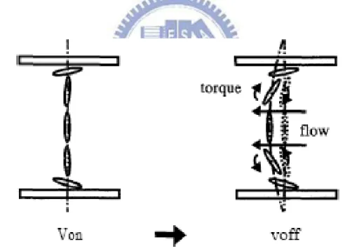
In Fig. 2-A, OCB cell‘s structure and five configurations are shown [25-27]. For an OCB cell, it usually consists of two ITO glasses as the upper and bottom substrates. The alignment layer on top of the substrate helps liquid crystals inside to align, and the pretilt angle is around 6 to 14 degree, such pretilt angle makes the LC molecules align in splay state in a plane without distortion. The normal state for OCB as a result will be splay state. When applied a voltage above the threshold voltage, the splay state would turn into symmetric splay state (also called Hs state) or asymmetric splay state (also called Ha state). When a voltage above the critical voltage applied, the cell would have a nucleation and change to bend state, that‘s where the liquid crystals were operated for OCB cell. After the applied voltage released, the cell would become 180° twist state first before it goes back to splay state.
Splayed ground state V>Vc1 Symmetric H state Glass Polyimide Asymmetric H state Bend state Twist state V>Vc2 Nucleation ITO V<Vc2 Nucleation Operation state V Bright Dark
15
-Hs state and Ha state is a transient state, when the tilt angle on both substrates is the identical, the cell would turn into Hs state, otherwise, the cell would turn into Ha state. Vc1 in
the figure usually would be 1Vrms, and Vc2 is around 2Vrms for most materials. The bend state
is topologically different from splay state, that‘s the reason for a nucleation process and usually takes few seconds to minutes to complete the transition. The twist state to splay state process for conventional twisted nematic device usually takes longer than OCB cell because of the backflow-induced alignment phenomenon [28]. OCB cell has symmetry pretilt angle on each surface and causes the flow which produces no backwards torque on the director near the center of the cell, and eliminates the adverse effects of flow alignment. This phenomenon can be explained by Van Doorn [29] using the numerical solution of the Ericksen-Leslie equations [30]. Fig.2-B shows the torque which induces by the flow accelerates the relaxation.
Fig. 2-B: Schematic figure of the dynamics in the pi-cell. The flow induces the torque to accelerate to relax. [31]
16
-2-1-2 FAST RESPONSE
One of the famous advantages of OCB cell is fast response [32-33].OCB cell operates in bend mode as Fig. 2-C (b) and homeotropic state as Fig.2-C (c) show. Since the alignment between these two states is alike, the response time is fast. Plus the no backward torque as mentioned earlier when removed the voltage, the response time is about 1 to 10ms, faster than TN mode (50 ms) and the response of human eyes (20 ms).
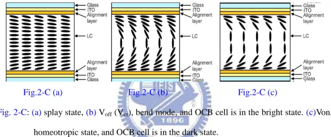
Fig.2-C (a) Fig.2-C (b) Fig.2-C (c)
Fig. 2-C: (a) splay state, (b) Voff (Vcr), bend mode, and OCB cell is in the bright state. (c)Von,
homeotropic state, and OCB cell is in the dark state.
2-1-3WIDE VIEWING ANGLE
Another advantage of OCB cell is wild viewing angle. From Fig. 2-D, compare TN mode
with OCB mode, the transmittance is 50%, the curve of TN mode has asymmetric distribution, while the curve of OCB cell has symmetric distribution. TN mode LCD is difficult to compensate the birefringence because of the complicated alignment structure. From the cross-section view of OCB cell in Fig. 2-E, the alignment of LC molecules is symmetric in the vertical direction and experience the same optical path along the symmetric direction in this plane. There is self-compensated effect in this direction. Therefore, the horizontal viewing angle of π cell is wider and symmetric than TN mode.
17
H o r i z o n t a l
V e r t i c a l
O C B
TN
Fig. 2-D: Experimental results of the viewing-angle-dependent transmittance for TN cell and OCB cell [11].
18
-2-1-4 NUCLEATION AND PHASE TRANSITION
As mentioned in earlier section, when applying a high voltage to the OCB cell, the splay state would transit to bend state. It is found that the transition is divided into two stages [34]. Fig. 2-F explains the process. Because of the topologically difference between these states, the transition starts with breaking the anchoring symmetry at the cell surfaces and forming a bend domain with a disclination loop around it. It clearly demonstrates it in the simulation by P. J. Bos et al. [35]. The velocity of the disclination lines motion can be calculated from the energy difference of the two states. The energy difference of the two states can be obtained in a simple formulation, called Boundary-Layer Model [36-37]. The declination lines finally annihilate with each other when the transition is completed.
Fig. 2-F: Mechanism of bend transition [34].
Bend transition cores can be generated by defects and structures such as spacers [38]. When applied voltage, anisotropic structures around the spacers by adsorption are able to nucleate the bend state.
19
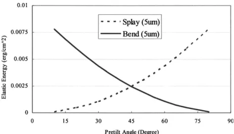
-Fig. 2-G: The pretilt angle versus energy distribution of splay state and bend state.
In Fig.2-G, the relation between Elastic energy and pretilt angle are presented. From this point, when the pretilt angle is larger, the elastic energy of splay state and bend state will be closer [39-40] and become easier to transit or don‘t even need a transition. When the pretilt angle is around 45 to 50 degree, the energy of these two states is almost the same. Since the pretilt angle of conventional OCB cell is around 6 to 14 degree, the elastic energy is smaller than bend‘s. Applied voltage will change the original energy distribution like Fig. 2-H shows.
20
-Therefore, we usually need to applied a voltage larger than critical voltage to the OCB cell for a while and wait the cell to transit to the higher energy bend state. It usually takes seconds to minutes to fulfill the process. The larger the voltage, the fast the process, however, too large voltage will not be suitable for TFT-drivers [41-42].
After the nucleation, the voltage corresponding to the 100% transmittance is called critical voltage (Vcr), and the voltage corresponding to the 0% transmittance is called dark
state voltage, OCB cell usually operates between these two voltage.
Some methods have been brought out to solve the phase transition issue, in addition to those mentioned in the introduction, there are still some other examples like generate bend core or chiral dopant [43-44] or multi-dimensional alignment [45] and offer a twist electric field[46]…etc. These methods may shorten the transition time but sacrifice some innate advantages of OCB cell.
2-1-5 LIGHT LEAKAGE IN DARK STATE
The pretilt angle of OCB is usually around 6 to 14 degree. Compare to VA mode displays, the pretilt angle is 90 degree. When applied a voltage higher than critical voltage and make OCB cell become homeotropic or dark state, the liquid crystals near the substrates suffer huge
constrained strength from the PI layer, and couldn‘t stand up like the VA mode displays. Fig.
2-I could explain the arrangement of VA and OCB mode. As a result, there will be a light leakage in the dark state. The contrast ratio will be lower than the VA mode, even with an additional compensation film. This phenomenon causes a weakness of OCB cell in the dark state.
21
Fig. 2-I (a) Fig. 2-I (b)
Fig. 2-I: The LC molecules alignment of (a) VA mode, and (b) dark state of OCB cell.
2-2SUMMARY
In this chapter, some of the details of OCB cell were introduced. OCB cell maintains many advantages, such as fast response time and wild viewing angle. Unfortunately, the fast response means operate in ‗bend mode‘, and needs a phase transition to become bend mode. The transition time could be long if the driving voltage is low, but high voltage is not suitable for TFT-driving devices. On the other hand, the contrast ratio is poor than VA mode displays, and light leakage could cause power consumption waste. Based on the good side of OCB cell, it is worth to improve the OCB cell and make it more applicable for the liquid crystal display.
22
-CHAPTER 3
MEASUREMENT SYSTEMS
The measurement systems that can help us get the E-O characteristics of the cell and the cell structures will be introduced in this chapter. The first one will be Atomic force microscope; it can help us to measure the thin film‘s thickness and surface condition. The second one will be UV/Vis spectrometer; this machine can help us measure the OCB cell‘s transmission spectrum and analyze the cell gap by interferometric method. The last but not least one will be the laser optical system; this one can measure the electro-optic characteristics and shows the relationship between voltage and cell‘s transmittance.
3-1 ATOMIC FORCE MICROSCOPE
The atomic force microscope (AFM) consists of a flexible micro-scale cantilever with a scanning sharp tip at its end that is used to scan the specimen surface, and use feedback mechanisms that enable the piezo-electric scanners to maintain the tip at a constant force. The cantilever is typically silicon or silicon nitride with a tip radius of curvature on the order of nanometers. The tips typically have an end radius of 2 nm to 20 nm, depending on tip type. When the tip is brought into proximity of a sample surface, forces between the tip and the
23
-sample lead to a deflection of the cantilever according to Hooke's law. Depending on the situation, forces that are measured in AFM include mechanical contact force, Van der Waals forces, capillary forces, chemical bonding, electrostatic forces, magnetic forces, Casimir forces, solvation forces etc. Typically, the deflection is measured using a laser spot reflected from the top of the cantilever into an array of photodiodes.
The scanning motion is conducted by a piezoelectric tube scanner which scans the tip in a raster pattern with respect to the sample (or scans to the sample with respect to the tip). The tip-sample interaction is monitored by reflecting a laser off the back of the cantilever into a split photodiode detector. By detecting the difference in the photo-detector output voltages, changes in the cantilever deflection or oscillation amplitude are determined. The schematic diagram of this mechanism is depicted in Fig. 3-A (a) and (b).
Fig. 3-A (a) Fig. 3-A (b)
Fig. 3-A: (a) Block Diagram of Atomic Force Microscope (b) Concept of AFM and the optical lever.
24
-There are 2 major operation modes for AFM:
I. Contact mode
Contact mode is the most common method to operate the AFM. But as the term suggests, the tip and the sample remain in close contact as scanning proceeds at this mode. One of the drawbacks of remaining in contact with the sample is that there exist large lateral forces on the sample as the drip is "dragged" over the specimen. It consists of scanning the probe across a sample surface while monitoring the change in cantilever deflection with the split photodiode detector. A feedback loop maintains a constant cantilever deflection by vertically moving the scanner to maintain a constant photo-detector difference signal. The distance the scanner moves vertically at each x, y data point is stored by the computer to form the topographic image of the sample surface. This feedback loop maintains a constant force during imaging, which typically ranges between 0.1 to 100 nN.
Non-contact mode
Non-contact operation is another method which may be employed when imaging by AFM. The cantilever must be oscillated above the surface of the sample at such a distance that we are no longer in the repulsive regime of the inter-molecular force curve. This is a very difficult mode to operate in ambient conditions with the AFM.
II. Tapping mode
It is the next common mode used in AFM. The cantilever is oscillated at its resonance frequency (typically ~300 kHz) and positioned above the surface so that it only taps the surface for a very small fraction of its oscillation period when operated in air or other gases. The laser deflection method is used to detect the root-mean-square (RMS) amplitude of cantilever oscillation. A feedback loop maintains constant oscillation amplitude by moving the
25
-scanner vertically at every x, y data point. Recording this movement forms the topographical image. This is still contact with the sample in the sense defined earlier, but the very short time over which this contact occurs means that lateral forces are dramatically reduced as the tip scans over the surface. The advantage of tapping mode over contact mode is that it eliminates the lateral, shear forces present in contact mode, enabling tapping mode to image soft, fragile, and adhesive surfaces without damaging them, which can be a drawback of contact mode AFM. In this thesis, the tapping mode AFM was used.
The Contact Mode and Tapping Mode are the most common ones because it can conduct in air or liquid environments.
Using AFM has several advantages as follows:
First, the samples don‘t need any special treatments such as metal coating, etc before they viewed by AFM. That will be very convenient and need not to worry the surface might be damaged by the additional treatment.
Second, AFM can operate in ambient air or liquid environment perfectly. There is no need to change the environment into a specific condition.
Third, AFM can provide a higher resolution than SEM and provide 3 dimensional surface profiles. On the contrary, SEM can only provide image or projection in 2 dimensions.
There are several disadvantages, too. For example, the AFM image‘s maximum height is smaller than SEM‘s. Second, an incorrect choice of tip for the required resolution can lead to image artifacts.
3-2 CELL GAP MEASUREMENT SYSTEM
The sample‘s thickness matters a lot in liquid crystal display and in our research. Before filled in liquid crystal in our hollow samples, we need to use UV/Vis spectrometer LAMBDA 950 from Perkin Elmer to measure the spectra of the samples and calculate the thickness by
26
-interferometric method [47].
LAMBDA 950 from Perkin Elmer, is shown in Fig. 3-B, can measure the spectrum from
Ultraviolet light to visible light, and from 175nm to 900nm, with the resolution ≦ 0.17 nm, and the spectrometer features a double-beam, double monochromator, and ratio recording optical system.
For applications such as sun protection, reflectance properties of flat panel display screens, paint films, transmission and reflectance characterization of glass and solar cells.
Fig. 3-B: UV/Vis spectrometer LAMBDA 950 from Perkin Elmer
As for the interferometric method, some basic concepts are introduced as follows.
For interferometric method, we need two reflective surfaces, as shown in Fig. 3-C. R1 is the reflective index of surface 1 and R2 is the reflective index of surface 2. When incident light passes through surface1 and 2, there will be an interference of light.
27
-Fig. 3-C: Two surfaces possess reflective index R1 and R2, light would pass through surface 1 and 2 and causing a light interference.
If total incident light is I=cos (ωt) and assume no absorption of light in surface 1and 2, then the total reflected light R can be written as Equation (3-1):
k
o
k k k kt t R R R t R R
1 cos cos 1 1 1 2 1 1 1 Equation (3-1) c n d t 2 gap gap2/ 1 0 Equation (3-2) 2 c ngap / Equation (3-3)Where c is the speed of light in vacuum, λ is the wavelength, dgap is the thickness of the layer,
and ngap is the refractive index of the layer.
The cosine factor k represents internal reflections for k>1, and the internal reflections can be neglected since the magnitude of k>1 when R1 and R2 will be smaller than 1 is much smaller than k=0. Therefore the Equation (3-1) can be rewritten asEquation (3-4):
ngapdgap t R R t RR 1cos 1 1 2 2cos 4 Equation (3-4)
Thus the reflected spectrum is
2 R12
1 R1
2R2
2 2R1
1 R1
2R2 cos
4ngapdgap/
R Equation (3-5)
The periodic term in Equation (3-5) causes an interference pattern. The periodicity of the reflected interference spectrum determined the optical thickness of the cell gap, ngap and dgap.
R1 I light incident layer n , dgap gap 1 R1 -1 (1-R1)R2 R2 R1) -(1 2 R2 R1) -R1(1 2 1 surface 2 surface
28
-If λ1and λ2 are the two wavelengths showing extrema in Equation (3-5), then we can
derive Equation (3-6), (3-7), (3-8) for λ=λ1 and λ=λ2.
4 /
1cos ngapdgap Equation (3-6)
2 /
2ngapdgap k11 Equation (3-7)
2 /
2ngapdgap k22 Equation (3-8)
Where k1 and k2 are natural numbers.
Suppose λ1> λ2, then for x is a nature number, k2 can be presented as Equation (3-9).
x k
k2 1 Equation (3-9)
Based on Equation (3-7), (3-8), and (3-9), we can write
1 2
2 1 4 x dngap gap Equation (3-10)
The value of x-1 indicates the number of extrema in R
2 between the wavelengths λ1and λ2. It is better to choose the distance x between the two extrema as large as possible to
improve the preciseness of the calculation of ngap dgap. We present a sample‘s result measured
by UV/Vis spectrometer LAMBDA 950 as an example, the spectrum is shown in Fig.3-D.
29
-From the figure, the sample has the following parameters, λ1=786, λ2=494, x=12, and the
result is shown inEquation (3-11)
3.98 m 494) -(786 4 494 786 12 4 1 2 2 1 x dngap gap Equation (3-11)
3-3 LASER OPTICS SYSTEMS
Fig. 3-E: the scheme of laser optic system.
We use laser optic system show as Fig.3-E to measure the electro-optic characteristics of our RMM-OCB cell. The major measurements include Voltage versus Transmittance, retardations, and response time.
We use He-Ne laser with wavelength equals 632.8nm as our laser source. After we put our sample in the middle of polarizer and analyzer, the laser would pass a 10% ND filter first to degrade the intensity into an acceptable range for photo detector. Then the laser would travel trough the polarizer, cell, analyzer, and finally to the photo detector. The laser light
pe Oscillosco tor Photodetec Analyzer Polarizer Sample filter ND Laser Ne -He generator Waveform Multimeter PC Program data data data Signal Signal Signal Signal
30
-would become a polarized light after passed through the polarizer. Based on the birefringence characteristic of liquid crystals, it possesses a △ n when light passes through and causes retardation, like a phase modulator. The polarized laser light would pass through the liquid crystal cell and change the phase depend on 2π△ nd/λ. Finally, the polarized light would pass through the analyzer and received by the photo detector. The photo detector PIN20 (from FLC Electronics AB) can detect any signal with its response more than 40ns. Then the oscilloscope (from Tektronix) would get the signals and digitized it and read by a Signal Multimeter (from Keithley), and then transfer the signals to the PC.
WFG500 (from FLC electronics AB) is a multi-channel high voltage waveform generator. The range for the maximum output voltage is ±100V and the minimum designable pulse width is 200ns. We also wrote a program called ‗FLC‘ to drive the LC cell by WFG500 (from FLC electronics AB) and connected with PC through GPIB interface. The frequency and waveform applied to the cell will be 1k Hz square wave for the voltage versus transmittance measurement.
When measuring the retardation of the cell, a compensator (Soleil-Babinet, From Special Optics, Model:8-400-UNCOATED) would be put in the middle of polarizer and analyzer,
like Fig.3-F. We would rotate the compensator and record the two minimum signals
detected by photo detector, and set them as min1 and min2.
Fig. 3-F (a)
Fig. 3-F (b)
31
-The cell would be put in the middle of polarizer and compensator like Fig. 3-F (b), and
rotate the compensator to record the minimum signal ‗x‘ that detected by photo detector. By substitute the ‗x‘ value into Equation (3-12) we can get the retardation value.
Retardation value =Γ=(x-min2) ÷ (min1-min2) Equation (3-12)
Moreover, with Equation (3-13) as followed, d means cell gap or film‘s thickness, we can even derive the cell‘s △ n with cell gap (d) or opposite.
Retardation value nd 2 360 2 Equation (3-13) d nvalue retardatio n 360 Equation (3-14)
3-4 POLARIZED OPTICAL MICROSCOPE (POM)
32
-The polarized optical microscope (POM) Olympus BX51 is designed to observe and photograph specimens that are visible primarily due to their optically anisotropic characteristic. Besides, transparent and reflective specimens can both be observed by this POM. In this instrument, the light would travel through a polarizer before it passes the specimens, and then an analyzer. Optical images will be monitored with a charge-coupled device (CCD) camera connected to a Personal computer. We have different choices on the magnifications and object lens, 100x, 200x, 500x, and 1000x for the first one, and 10x,20x,50x,and 100x for the second one, and a 10x for the ocular lens.
33
-CHAPTER 4
EXPERIMENTS AND RESULTS
In application, OCB cell has two main advantages that degrade its performance, first one will be critical voltage‘s existence and the second one is insufficient dark state. OCB cell needs a high pulse voltage to transit its splay state into bend state to operate, and the alignment of OCB cell has more light leakage than other liquid crystal cells, for example, TN, VA, and IPS. Insufficient dark state will cause the contrast ratio inadequate, too.
In this essay, an additional layer made by nematic acrylate mixture (also called RMM-19B, from Merck Co.) were coated on top of the PI layer and formed a higher pretilt angle. Since the pretilt angle has a negative relationship with the transition voltage [48], the transition voltage can be removed successfully. Moreover, the additional RMM layer can make the dark state darker than before. The details will be discussed later in this chapter.
34
-4-1 CELL FABRICATION PROCESS
Fig. 4-A shows the procedure of OCB cell‘s fabrication:
Fig. 4-A: Fabrication process of OCB cells.
A. The glasses that been used in this thesis are all pre-coated by Indium-Tin-Oxides (ITO)
to make the glasses conducted. After cut the ITO glasses into small pieces of glasses that have 2cm × 2.5cm areas, 5wt% detergent solution are been used to clean the glass's surfaces. This process usually took an hour and an half for 20 small pieces of glasses. Afterward, the clean glasses will be put into a supersonic cleaner for 30minutes. To dry off the glasses, Nitrogen will be used to blow over the surfaces first, and then baked for 1 hour.
G: Measure Cell Gap A: ITO glass clean
B: Spin coating alignment layer
C: Baking and rubbing
I: Measurement H: LC injection F: Form Cell D: Coating RMM-19B
35
-B. A solution that compound with polyimide (Chisso PIA-5580-01) and solvent were made.
The ratio of the mixture solution will be PI: Solvent equals 3:1. The pretilt angle of the polyimide is around 7°. In the same time, the dry ITO glasses will be put into an UV-Ozone for 20 minutes to increase the hydrophile of the surfaces. After that, the mixture solution were filled into a glass syringe and put on a 0.2um filter to leach extra particles. Then drip the mixtures on glasses and use a spin coating machine to create the uniformity of the polyimide. The parameters of the spin coating are given as Table 4-A.
Table 4-A. Parameters of spin coating polyimide
Speed Time
Solvent-Waiting 0rpm 30secs
Solvent-1st spin 800rpm 30secs
Solvent-2nd spin 5000rpm 60secs
Polyimide mixture solution-Waiting 0rpm 30secs
Polyimide mixture solution -1st spin 800rpm 30secs
Polyimide mixture solution -2nd spin 5000rpm 60secs
C. After the glasses with PI on the surfaces were backed 220℃ 1 hour. Rubbing machine
with the following parameters (Table 4-B) will be rubbed on the sample glasses.
Table 4-B. Rubbing Conditions for Polyimide glasses
Pile impression 0.2mm
Rotation speed 500rpm
36
-D. The following step is coating RMM-19B (from Merck Co.) on the PI layer. RMM-19Bis
in solid state when in room temperature. After dissolved the RMM-19B into PGMEA and make 2 different concentrations to do the experiment, 1st one is 2wt%, 2nd one is 4wt%. The results of 2wt% are not good as the 4wt% one, so the following results are going to discuss the 2nd concentration only.
Again, the glass syringe and 0.2um filter was used. Then RMM-19B will be dripped on the PI layer, and use a spin coating machine to create the uniformity of the RMM layer. The parameters of the spin coating are given in Table 4-C.
Table 4-C. Parameters for RMM-19B
Time Speed
1st spin 30s 500rpm
2nd spin 60s Sample-1 & cell-1 Sample-2 & cell-2 Sample-3 & cell-3
6000rpm 4000rpm 2000rpm
E. After coating, the sample were backed with 40℃ to 50 ℃ and exposed to an UV light in
the same time for 5 to 10 minutes to solidify the RMM layer.
F. The novel RMM cell structure has two different attempts in the substrate choices, the
substrates with only PI on it or the substrates with additional RMM layer on top of the PI layer. The first type, called RMM-OCB cell, used only PI layer on it as the upper substrate and additional RMM layer as the bottom substrate. The second type, called RMM2-OCB cell, used additional RMM layer on both bottom and upper substrates. The types can be interpreted by Fig. 4-B.
37
-Fig. 4-B (a) Fig. 4-B (b)
Fig. 4-B the two different types: (a) only the bottom substrate uses RMM layer glasses. (b) Both substrate use RMM layer on it.
Additionally, the spacer that used to seal the cells were mixed with UV glues (NOA-65, from Norland). For both cell types, we fabricated with two different spacers, 3.5μm and 5μm. After sealed with spacer mixtures and exposed to UV lamp for 5 minutes. The cells are read to measure the cell gaps by spectrometer.
G. The cell gap of the empty cells was measured by UV/Vis spectrophotometer Lambda
950 (from Perkin Elmer). The machine‘s faculty has been explained in the previous chapter completely.
H. Afterward, the nematic liquid crystal, ZCE-5096XX (from Chisso), was injected into the
cell by capillarity. The details of the liquid crystal were given as Table 4-D.
Table. 4-D. The parameters of liquid crystal ZCE-5096XX
Sample ZCE-5096XXXX
TN->C[S] <-20 ℃
TN->I 95.5 ℃
38
-Table. 4-D. The parameters of liquid crystal ZCE-5096XX (conti.)
Optical anisotropy (at 25℃ 589nm)
△ n 0.158
ne 1.662
no 1.504
Dielectric anisotropy (at 25℃)
△ ε 10.0
ε|| 14.1
ε⊥ 4.1
Specific resistivity ρ (at 25℃) >1.5*1014Ω.cm
K11 9.8 dyne
K22 5.8 dyne
K33 11.8 dyne
γ1 178 mPas
I. After soldered conducted wires on surface, the different types of cells were be able to
measure the E-O characteristics.
4-2 CHARACTERISTICS OF REACTIVE NEMATIC LC MONOMERS
The reactive nematic liquid crystal monomers (from Merck Co.), also called RMM-19B or RMM for short, is a polymerizable nematic acrylate mixture, and was given a splay alignment. The mixture contains LC molecules and polymerization monomers that can be polymerized by UV irradiation or UV light exposure and became solidify on the surface. Since RMM-19B is also a LC material which provides phase retardation of linearly polarized light.
39
-4-3 NOVEL OCB-CELL MODEL
The novel cell structure has RMM layer on top of the PI alignment layer. The
RMM-OCB cell (first type) structure was shown in Fig. 4-C. From the figure, the additional
RMM layer was able to achieve a higher pretilt angle on the substrate. As a result, a transition free OCB cell was obtained with high surface pretilt angle on the substrate [49-50]. Moreover, the RMM layer with residual retardation and easily aligned vertically at high voltage could improve the cell‘s contrast ratio. The novel structure can solve the phase transition issue and the drawback of contrast ratio at the same time.
Fig.4-C (a) Fig.4-C (b)
Fig.4-C The scheme of RMM-OCB cell under (a) 0V, (b) 6V
In order to know the uniformity and thickness of the additional RMM layer, AFM and polarizing optical microscope (also called POM for short) were used. In Fig. 4-D and
Table.4-E, the uniformity and the thickness of the RMM layer were measured by AFM. The
dark and bright state were measured by POM and showed in Fig. 4-E. From AFM and the pictures taken by POM, RMM-19B has good uniformity on top of the PI layer.
40
-Fig. 4-D: RMM-19B microscopic structure observed by AFM. RMM-19B forms a thin film about 100~200 nm with 3 nm roughness.
Table. 4-E: RMM thickness with spin coating speed’s relation
Spin Coating Speed 6000 rpm 4000 rpm 2000 rpm 500 rpm
RMM thickness 80nm 110nm 134nm 200nm
Fig. 4-E (a) Fig.4-E (b)
41
-4-4 MEASUREMENT OF ELECTRO-OPTICAL PROPERTIES AND
RESULTS
4-4-1 PHASE TRANSITION FREE OCB CELL
The RMM-OCB cell that only has bottom substrate with additional RMM layer on it got
the following results. If the cell gap of RMM-OCB cell is around or larger than 5 m, there
will be no phase transition when RMM layer is thicker than 130 nm. As for cells with cell gap
equals 3m, all of them are transition free. The relationship between RMM layer‘s thickness
and critical voltage were examined by AFM and the results are showed in Fig. 4-F. The thickness of PI layer is around 75 nm.
-0.1 0 0.1 0.2 0.3 0.4 0.5 0.6 0.7 80 90 100 110 120 130 140 150 160 Fig. 4-F
with 5um spacer with 3um spacer
C ri ti cal V ol tage Thickness of RMM layer (nm)
Fig. 4-F: the relation between the RMM layer‘s thickness and the cell‘s Critical voltage corresponds to different spacers.
From the figure, for cell‘s cell gap equals or bigger than 5m, the critical voltage will decrease while the RMM layer‘s thickness increases. Nevertheless, for those RMM-OCB cells have cell gaps equal or less than 3 m, they were able to be driven without the phase
42
-transitions. As for the relation between critical voltage with the spacers and with the thickness, the data is summarized in Table.4-F and Table.4-G. The RMM-OCB cell were put in the middle of the polarizer and analyzer in the laser optical system to measure the transmittance and V-T curve, like Fig. 4-G, the θ will be 45°.
Fig. 4-G: the include angle θ=45° between RMM-OCB cell‘s rubbing direction and
polarizer‘s direction.
Table. 4-F: 4wt% RMM-OCB cells and conventional OCB cell-1 (cell gap ~ 5.0±0.05um)
Cell name OCB Cell-1 Cell-2 Cell-3
RMM thickness None 90nm 110nm 134nm
Critical voltage 1.6V 0.6V 0.2V 0.0V
*without using compensation films, OCB means conventional OCB cell
Table.4-G: 4wt% RMM-OCB cells and conventional OCB cell-2 (cell gap ~ 3.2±0.05um)
Cell name OCB Sample-1 Sample-2 Sample-3
RMM thickness None 90nm 110nm 134nm
Critical voltage 1.6V 0.0V 0.0V 0.0V
*without using compensation films, OCB means conventional OCB cell
θ
Rubbing Direction
Polarizer
43
-The V-T curves in Fig. 4-H (a) and Fig. 4-H (b) are corresponded to 5 m and 3 m cell gaps. From Fig. 4-H (a) & (b), the dark state of RMM-OCB cells are darker than the conventional OCB cell. In other words, the RMM-OCB cell suppressed more light leakage at oblique incidence than conventional one. As a result, the contrast ratio had improved greatly.
0 20 40 60 80 100 0 2 4 6 8 10 cell-2 cell-3 OCB cell-1 T ran sm it tan ce( % ) Applied votage(V) Fig. 4-H(a) 0 20 40 60 80 100 0 2 4 6 8 10 sample-1 sample-2 sample-3 OCB T ra n s m it ta n c e (% ) Applied voltage (V) Fig. 4-H(b) -20 0 20 40 60 80 100 120 0 2 4 6 8 10 Fig. 4-H (c) Conventilonal OCB RMM layer on both sides
T ran smi ttan ce (% ) Applied Voltage (V)
Fig. 4-H: Different thickness of RMM layers with (a) cell gap around 5um, and (b) cell gap
around 3um, and (c) RMM layer on both substrates.
On the contrary, when measuring RMM2-OCB cell‘s transmittance and put the cell in the laser optic system, too. The system cannot let any light pass trough and got nothing on the V-T measurement. The results are presented in Fig. 4-H (c). This result pointed out the pretilt angle on the additional RMM layer may be high enough and causes liquid crystals inside
44
-became homeotropic. The calculation of RMM layer‘s pretilt angle will be shown later in this chapter. To prove the homeotropic state in RMM2-OCB cell, the include angle ‗θ‘ between cell rubbing direction and the polarizer were changed and measured the transmittance in the same time. The results are presented in Table.4-H. From the results, the liquid crystals inside RMM2-OCB cell are in homeotropic state.
Table. 4-H: the transmittance of RMM2-OCB cell when in different include θ
Angle(θ) 0 30 45 90 120 150 180 270
transmittance 0 0 0 0 0 0 0 0
4-4-2 RETARDATIONS
The retardations of both RMM-OCB cells and conventional OCB cell were measured by He-Ne laser (λ=632.8nm). As shown in Fig. 4-H, the conventional OCB cell has a similar retardation curve compared with RMM-OCB cell when the driving voltage was higher than critical voltage. 0 50 100 150 200 250 300 350 -40 -30 -20 -10 0 10 20 30 40 6V 4V 3V 2V 1.8V 0V Re ta r da tio n( de g r ee ) Rotated angle(degree) Fig. 4-I(a) 0 50 100 150 200 250 300 350 -40 -30 -20 -10 0 10 20 30 40 RM-4V RM-6V RM-3V RM-2V RM-1.8V RM-0V Re ta r da tio n( de g ree ) Rotated angle(degree) Fig. 4-I(b)
Fig.4-I (a) is conventional OCB cell‘s retardation. Fig.4-I (b) on the right is retardations of the RMM-OCB cells under applied voltage from 0V to 6V with different viewing angle.

![Fig. 2-D: Experimental results of the viewing-angle-dependent transmittance for TN cell and OCB cell [11]](https://thumb-ap.123doks.com/thumbv2/9libinfo/8598314.190017/27.892.153.769.146.934/fig-experimental-results-viewing-angle-dependent-transmittance-cell.webp)