A New Architecture for Charge Pump Circuit Without
Suffering Gate-Oxide Reliability in Low-Voltage
CMOS Processes
Tzu-Ming Wang, Wan-Yi Shen, and Ming-Dou Ker Nanoelectronics and Gigascale Systems Laboratory Institute of Electronics, National Chiao-Tung University
HsinChu, Taiwan
Abstract—A new architecture of charge pump circuit without
suffering gate-oxide reliability in low-voltage CMOS processes is proposed, which is composed of two identical pumping branches and four-phase clock signals. The four-phase clock signals are designed to have no undesirable return-back leakage path during clock transition and to control the charge transfer MOSFET switches in the proposed circuit to be turned on and off completely. Therefore, its pumping efficiency is higher than that of the conventional one. Because the gate-to-source and gate-to-drain voltages of all devices in the new proposed charge pump circuit do not exceed the normal power supply voltage (VDD), the new proposed charge pump circuit is suitable for applications in low-voltage CMOS processes.
I. INTRODUCTION
Charge pump circuits play an important role in memory applications such as EEPROMs, SRAMs, DRAMs and flash memories. Many charge pump circuits are designed according to the circuit proposed by J. F. Dickson [1]. Charge pump circuits are usually used to generate a voltage which is higher than the normal supply voltage or lower than the ground voltage to program, read, or erase the floating-gate devices in the flash memories and EEPROMs [1]-[4]. Besides, the negative voltages may be applied to reduce leakage current for SRAMs and DRAMs. These applications require the higher or the lower voltage level with smaller current drivability. However, for the recent applications such as USB OTG (On-The-Go), require not only the higher voltage but also the higher current drivability.
Fig. 1 shows a conventional four-stage Dickson charge pump circuit using diode-connected MOSFET as the charge transfer device to push the charges from one stage to another in one direction. In Fig. 1, the charges are transferred from the power supply (VDD) to the output node (Vout) and pumped by the two out-of-phase clock signals (CLK and CLKB) stage by stage. Thus, the output voltage of the charge pump circuit can be pumped higher than the normal power supply voltage. The voltage fluctuation at each pumping node can be expressed as
Figure 1. A conventional four-stage Dickson charge pump circuit.
(
par)
CLK o par CLK f V C CC f CI C V + ⋅ − + ⋅ = (1)where VCLK is the voltage amplitude of the clock signals, C
is the pumping capacitance, Cpar is the parasitic capacitance
at each pumping node, Io is output current, and fCLK is the
clock frequency.
In general, the parasitic capacitance is much smaller than the pumping capacitance. If output current is also small enough, Cpar and Io can be ignored in (1). Because the
voltage level of VCLK is usually identical to the power
supply voltage (VDD), the voltage fluctuation of each pumping node is about VDD. Hence, the output voltage of the conventional four-stage Dickson charge pump circuit is expressed as
(
)
∑
= − + = N 1 i t(i) CLK V V VDD Vout (2)where VCLK is about VDD as mentioned above, N is number
of stages, and Vt(i) denotes the threshold voltage of the
diode-connected MOSFET Mi. Traditionally, the bulk terminals of the diode-connected MOSFETs in the Dickson charge pump circuit are connected to ground. When the voltage on each pumping node is pumping higher, the threshold voltage (Vt(i))
is larger due to the body effect. Therefore, the pumping gain of the Dickson charge pump circuit is limited by the body effect as the number of stages is increased. Since the threshold voltage cannot be scaled as much as the scaling trend of the power supply voltage, the impact of this phenomenon becomes more serious in the low power supply voltage applications.
Figure 2. A charge pump circuit with consideration of gate-oxide reliability [6].
(a)
(b)
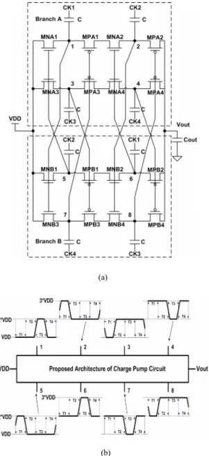
Figure 3. (a) The circuit scheme and (b) corresponding voltage waveforms for the proposed architecture of charge pump circuit.
The charge pump circuit with higher pumping gain and without suffering gate-oxide reliability is illustrated in Fig. 2. The detailed operation principle of Fig. 2 is described in [6]. The devices in this charge pump circuit have no gate-oxide reliability issue, but it could suffer a leakage path due to the simple two clock signals. As CLK signal is rising and CLKB is falling, it is expected that the voltage at node 1 and node 2 in Fig. 2 are respectively rising and falling as well. Because the MN1 is not completely turned off immediately, the voltage at node 1 holds at VDD until the voltage at node 2 is falling lower enough to completely turn off MN1.
To prevent the return-back leakage path during clock transition mentioned above, a new architecture of charge pump circuit without suffering gate-oxide reliability in low-voltage CMOS processes is proposed in this work.
II. PROPOSED ARCHITECTURE OF CAHRGE PUMP CIRCUIT
Figs. 3 (a) and (b) illustrate a new scheme of charge pump circuit and its corresponding voltage waveforms. The clock signals CK1, CK2, CK3, and CK4 have their voltage amplitudes as the power supply voltage (VDD) and their waveforms are similar to the nodes 1, 5, 3, and 7 respectively. The two identical branches are labeled as branch A and branch B in the proposed architecture of charge pump circuit. The only difference between these two branches is the order of the clock signals. If the clock signals of the first and the second pumping stages in the upper part of branch A are CK1 and CK2, the clock signals in the upper part of branch B should be CK2 and CK1. It is similar in the lower parts of branches A and B, so branches A and B can be viewed as two independent charge pump circuits and their output nodes are connected together. The detailed operations of the new proposed charge pump circuit are described below.
(a) (b)
(c) (d)
Figure 4. The simulated voltage waveforms of the (a) CK1, node 1, and node 6, (b) CK2, node 2, and node 5, (c) CK3, node3, and node 8, and (d) CK4, node 4, and node 7, in the proposed architecture of charge pump circuit with clock period = 1200 ns.
A. At Period T1
As shown in Figs. 3, at the time period T1, clock signals CK1, CK2, CK3, and CK4 are low, high, low, and high, respectively. For the first stage of the proposed charge pump circuit, the voltage difference between node 1 and 5 (V15) is –VDD and V35 and V17 are –VDD, too. Therefore, charge transfer MOSFET switches MNA1 and MNA3 are turned on to push the charges from VDD to node 1 and node 3, and MNB1 and MNB3 are turned off to block the charge transfer path from node 5 and node 7 back to VDD.
For the pumping stages, V17 and V26 (V37 and V46) are –VDD and VDD, respectively. MPA1 and MNA2 (MPA3 and MNA4) are turned off in order to prohibit the charge transfer path from node 2 (node 4) back to node 1 (node 3). V35 and V26 (V37 and V28) are –VDD and VDD, so MPB1 and MNB2 (MPB3 and MNB4) are turned on to transfer the charges from node 5 (node 7) to node 6 (node 8).
For the output stages, V28 and V48 are VDD, so charge transfer MOSFET switches MPA2 and MPA4 are turned on to push the charges from node 2 and node 4 to the output node. On the other hand, MPB2 and MPB4 are turned off to block the charge transfer path from the output node back to node 6 and node 8, because the voltage across the output node and node 4 is 0 V.
B. At Period T2(T4)
At the time period T2 (T4), CK1 is low, CK 2 is low, CK3 is high, and CK4 is high. For the first stage of the proposed charge pump circuit, V15 is 0, V35 is VDD, and V17 is –VDD for ideal operation. MNA1, MNA3, MNB1, MNB3 are turned off to block the charge transfer path from node 1, node 3, node 5, and node 7 back to VDD. For the pumping stages, MPA1, MNA2, MPA3, and MNA4 (MPB1, MNB2, MPB3 and MNB4) are turned off to prevent the charges transfer from node 2 (node 6) to node 1 (node 5) and from node 4 (node 8) back to node 3 (node 7).
For the output stages, MPA2, MPA4, MPB2, and MPB4 are turned off to impede the charge transfer path from output node back to node 2, node 4, node 6, and node 8.
C. At Period T3
At the time period T3, CK1 is high, CK2 is low, CK3 is high, and CK4 is low. For the first stage of the proposed charge pump circuit, V15, V35, and V17 are all VDD. MNA1 and MNA3 are turned off to block the charge transfer path from node 1 and node 3 back to VDD. MNB1 and MNB3 are turned on to push the charges from VDD to node 5 and node 7.
For the pumping stages, V53 and V62 (V73 and V82) are –VDD and VDD, respectively. Thus, charge transfer MOSFET switches, MPB1 and MNB2 (MPB3 and MNB4) are turned off to hinder the charge transfer path from node 6 (node 8) to node 5 (node 7). In addition, V17 and V26 (V37 and V46) are VDD and–VDD, so MPA1 and MNA2 (MPA3
and MNA4) are turned on to push the charges from node 1 (node 3) to node 2 (node 4).
For the output stage, V46 and V48 are –VDD, so MPB2 and MPB4 are turned on to push the charges from node 6 to node 8 to the output node. MPA2 and MPA4 are turned off to block the charge transfer path from the output node back to node 2 and node 4, because the voltage across the output node and node 8 is 0 V.
As shown in Figs. 3, gate-to-source voltage (Vgs) and gate-to-drain voltage (Vgd) of all devices in the proposed charge pump circuit do not exceed VDD. All devices do not suffer the gate-oxide reliability issue in this new charge pump circuit. If the process provides the triple-well technology, the bulk terminal of the devices used in the charge pump circuit can be connected to source terminal to avoid the overstress between gate terminal and bulk terminal. A 1.8-V 0.18-μm model is used to simulate and verify the design of the proposed architecture of charge pump circuits. Fig. 4 shows the simulated voltage waveforms of the nodes in the proposed architecture of charge pump circuit with clock period of 1200 ns. Each pumping capacitor is 1nF and the output capacitor is 1 μF. The simulation results in Fig. 4 agree to the expected waveforms of Fig. 3 (b). At node 1, node 3, node 5, and node 7, the voltage amplitude is between about VDD and 2xVDD. On the other hand, at node 2, node 4, node 6, and node 8, the voltage amplitude is between about 2xVDD and 3xVDD. Thus, all devices in the proposed architecture do not suffer the gate-oxide reliability issue because the maximum voltage difference between each terminal is only VDD.
(a) (b)
Figure 5. Simulated voltage waveforms of output node at VDD = 1.8 V and clock period = 1200 ns with output current of (a) 0 mA and (b) 0.5 mA.
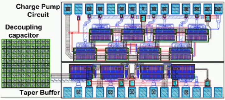
Figure 6. The layout of the proposed architecture of charge pump circuit.
Figs. 5 (a) and (b) show the simulated voltage waveforms of output node with the clock period of 1200 ns, the pumping capacitance of 1 nF, and the output capacitor is 1 μF. The charge pump circuit with higher output current has smaller output voltage.
The layout of the proposed architecture of charge pump circuit is illustrated in Fig. 6. The layout includes the charge pump circuit shown in Fig. 3(a), the taper buffer which is used to drive the large pump capacitances in each node, and the decoupling capacitor is between VDD and GND. Besides, this design eliminates the body effect by biasing the body terminals in all devices dynamically, so it is also suitable for low-voltage CMOS processes.
III. EXPERIMENTAL RESULTS
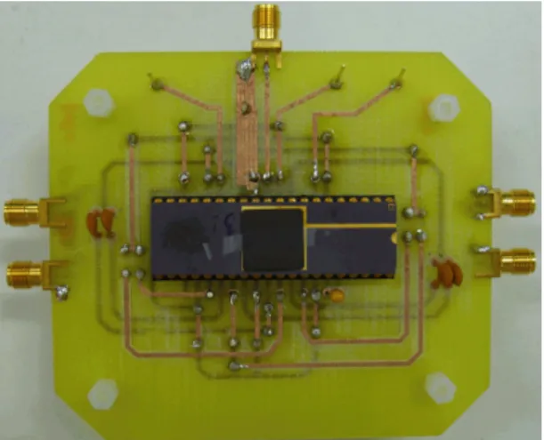
A new architecture of charge pump circuit without gate-oxide reliability issue in low-voltage CMOS processes has been fabricated in a 1.8-V 0.18-μm CMOS process. The photograph of test PCB with the fabricated charge pump circuit in IC package to verify the new proposed architecture is shown in Fig. 7. In Fig. 8, it shows the measured voltage waveforms on the output node (Vout) and CK1 with clock period of 1200 ns, supply voltage of 1.8 V, and the output loading (Rout) of 22 kΩ. The output voltage is about 4.4 V. Fig. 9 shows measured output voltage of the proposed architecture of charge pump circuit with different output current. The output voltage of proposed architecture of charge pump decreases as the output current increases.
IV. CONCLUSION
A new architecture of charge pump circuit without gate-oxide reliability issue in low-voltage CMOS processes has been designed and fabricated in a 1.8-V 0.18-μm CMOS process. In this new architecture, the gate-to-drain and the gate-to-source voltages of all devices do not exceed VDD. The proposed architecture of charge pump circuit would not suffer a return-back leakage path during clock transition.
Figure 7. The photograph of test PCB with the fabricated charge pump circuit in IC package to verify the new proposed architecture.
Figure 8. Measured voltage waveforms of the proposed architecture of charge pump circuit with VDD = 1.8 V and clock period = 1200 ns.
Figure 9. Measured output voltage of the proposed architecture of charge pump circuit with different output current.
REFERENCES
[1] J. F. Dickson, “On-chip high-voltage generation in NMOS integrated circuits using an improved voltage multiplier techniques,” IEEE J.
Solid-State Circuits, vol. 11, pp.374-378, June, 1976.
[2] M. Kuriyama, S. Atsumi, A. Umezawa, H. Banba, K.-I. Imamiyu, K. Naruke, S. Yamada, E. Obi, M. Oshikiri, T. Suzuki, M. Wada, and S. Tanaka, “A 5V-only 0.6μm flash EEPROM with row decoder scheme in triple-well structure,” in IEEE Int. Solid-State Circuits Conf. Dig.
Tech. Papers, 1992, pp. 152-153.
[3] T. Kawahara, T. Kobayashi, Y. Jyouno, S.-I. Saeki, N. Miyamoto, T. Adachi, M. Kato, A. Sato, J. Yugami, H. Kume, and K. Kimura, “Bit-line clamped sensing multiplex and accurate high voltage generator for quarter-micron flash memories,” IEEE J. Solid-State Circuits, vol. 31, pp. 1590-1600, Nov. 1996.
[4] N. Otsuka and M. A. Horowitz, “Circuit techniques for 1.5-V power supply flash memory,” IEEE J. Solid-State Circuits, vol. 32, No. 8, pp. 1217-1230, Aug. 1997.
[5] T. Tanzawa, Y. Takano, K. Watanabe, and S. Atsumi, “High-voltage transistor scaling circuit techniques for high-density negative-gate channel-erasing NOR flash memory,” IEEE J. Solid-State Circuits, vol. 37, pp. 1318-1325, Oct. 2002.
[6] M.-D. Ker, S.-L. Chen, and C.-S. Tsai, “Design of charge pump circuit with consideration of gate-oxide reliavility in low-voltage CMOS processes,” IEEE J. Solid-State Circuits, vol. 41, no. 5, pp.1100-1107, May 2006.