Low-resistance ohmic contacts on p-type GaN using Ni/Pd/Au metallization
Chen-Fu Chu, C. C. Yu, Y. K. Wang, J. Y. Tsai, F. I. Lai, and S. C. Wang
Citation: Applied Physics Letters 77, 3423 (2000); doi: 10.1063/1.1327276 View online: http://dx.doi.org/10.1063/1.1327276
View Table of Contents: http://scitation.aip.org/content/aip/journal/apl/77/21?ver=pdfcov Published by the AIP Publishing
Articles you may be interested in
Highly reflective low resistance Ag-based Ohmic contacts on p -type GaN using Mg overlayer Appl. Phys. Lett. 90, 012106 (2007); 10.1063/1.2430405
Low-resistance and high-reflectance Ni Ag Ru Ni Au ohmic contact on p -type GaN Appl. Phys. Lett. 85, 4421 (2004); 10.1063/1.1819981
Low-resistance Pt/Pd/Au ohmic contacts to p-type AlGaN Appl. Phys. Lett. 84, 1710 (2004); 10.1063/1.1668331
Low-resistant and high-transparent Ru/Ni ohmic contact on p-type GaN Appl. Phys. Lett. 80, 2937 (2002); 10.1063/1.1474609
Low-resistance Pt/Ni/Au ohmic contacts to p-type GaN Appl. Phys. Lett. 74, 70 (1999); 10.1063/1.123954
This article is copyrighted as indicated in the article. Reuse of AIP content is subject to the terms at: http://scitation.aip.org/termsconditions. Downloaded to IP: 140.113.38.11 On: Thu, 01 May 2014 07:39:12
Low-resistance ohmic contacts on
p
-type GaN using Ni
Õ
Pd
Õ
Au metallization
Chen-Fu Chu, C. C. Yu, Y. K. Wang, J. Y. Tsai, F. I. Lai, and S. C. Wanga)Institute of Electro-Optical Engineering, National Chiao Tung University, Hsinchu, Taiwan, Republic of China
共Received 28 August 2000; accepted for publication 20 September 2000兲
In this letter, a low-resistance ohmic contact on p-type GaN using an alloy of Ni/Pd/Au is reported. The Mg doped p-type GaN samples were grown by metalorganic chemical vapor deposition with a carrier concentration of 4.1⫻1017cm⫺3. The as-grown Mg doped samples were deposited with Ni
共20 nm兲/Pd 共20 nm兲/Au 共100 nm兲 and then annealed in air, nitrogen, and oxygen ambient conditions
at different annealing temperatures ranging from 350 to 650 °C. Linear I – V ohmic characteristics were observed with specific resistance as low as 1.0⫻10⫺4⍀ cm2 for the samples annealed in
oxygen atmosphere. Similar contact metal composition was also deposited on Be-implanted p-type GaN samples with a carrier density of 8.1⫻1019cm⫺3. Without further annealing process, the samples show good ohmic contact with a lowest specific resistance of 4.5⫻10⫺6⍀ cm2. © 2000 American Institute of Physics. 关S0003-6951共00兲01847-7兴
GaN based semiconductors have been applied to fabri-cate optoelectronic devices such as light emitting devices, metal–semiconductor field effect transistors, ultraviolet pho-toconductive detectors, and diode lasers.1–5One of the seri-ous concerns in particular for light emitting devices is the large voltage drop across the GaN/metal interface for ohmic contacts, which leads to poor devices performance.
For n-type GaN, ohmic contact with relatively low con-tact resistance of 10⫺5– 10⫺8⍀ cm2using alloy composition such as Ti/Au, Ti/Al, and Ti/Al/Ni/Au,6–8 have been achieved. However, for p-type GaN because of the difficulty in achieving high carrier density and the absence of suitable metals with high work function, a high-quality ohmic contact with low resistance is still relatively difficult to obtain. Many attempts have been reported thus far in finding ways of low-ering the contact resistance in p-type GaN materials. Re-cently, various Au-based ohmic contacts using metallization such as Ni/Au,9–11 Co/Au,12 Pd/Au,13 Pd/Pt/Au,14 Ni/Pt/Au,15 Pt/Ni/Au,16 and Ti/Pt/Au17 have been reported. These contact metallizations were either annealed in a nitro-gen and oxynitro-gen environment or without any annealing. The specific contact resistance (c) was typically in the range of 2.1⫻10⫺2to 4.2⫻10⫺5⍀ cm2. The reduction of contact re-sistance for the Au-based ohmic contacts annealed in N2and
O2atmosphere was attributed to either the removal of
hydro-gen atoms bounded to Mg or N atoms, or formation of an intermediate semiconductor layer such as p-NiO with high hole concentration. In this letter, we report a new contact metallization scheme using Ni/Pd/Au on p-type GaN in achieving linear current–voltage (I – V) characteristic with low ohmic contact resistance.
The Mg-doped p-type GaN samples were grown on sap-phire substrate by the metalorganic chemical vapor deposi-tion共MOCVD兲 system 共Emcore D75兲. A 1m thick p-type epilayer was grown on the 1 m thick undoped GaN. The carrier concentration of the as-grown p-type GaN measured
by Hall measurement was about 4.1⫻1017cm⫺3. Both circu-lar and annucircu-lar pads were patterned on the p-type GaN epi-layer by the standard photolithography technique for mea-surement of specific contact resistance using circular transmission line method共CTLM兲. The inner dot radius was 200m and the spacing between the inner and the outer radii were varied from 3 to 45m. A metal contact layer structure of Ni 共20 nm兲/Pd 共20 nm兲/Au 共100 nm兲 was deposited in sequence on the p-type GaN by electron beam evaporation under a pressure of 2⫻10⫺6Torr.
Samples of p-type GaN with metallization were then an-nealed in different ambient conditions including air, nitro-gen, and oxygen. The annealing temperature varies from 350 °C to 650 °C for 5 min to optimize the annealing condi-tions. Figure 1共a兲 shows the I – V characteristics for the samples annealed in air at different annealing temperatures. A near ohmic characteristic is obtained as the annealing tem-perature rises to 450–550 °C. As the annealing temtem-perature increases beyond 550 °C, the I – V curve becomes nonlinear again. Figure 1共b兲 shows I – V curves for samples annealed in a N2 atmosphere that have similar temperature dependence
as those annealed in air. Figure 2 shows the I – V curves of the samples annealed in O2atmosphere. The I – V curves for
annealing temperature below 550 °C show good linear ohmic behavior with low resistance characteristics. Total resistance against the pad distance measurement by CTLM for the samples annealed at 550 °C under different ambient condi-tions was plotted in Fig. 3. The specific contact resistance determined from the intercepts and slopes in the plots has a value of 1.1⫻10⫺2, 1.5⫻10⫺3, and 1.0⫻10⫺4⍀ cm2 for the sample annealed in air, N2, and O2, respectively. The results show that the samples annealed at 550 °C in oxygen have the best ohmic characteristic with a lowest specific re-sistance of 1.0⫻10⫺4⍀ cm2.
The same Ni/Pd/Au contact metals were also used to deposit on the Be-implanted p-type GaN samples. These samples were prepared by implantation of Be ions with en-ergy of 50 keV at a dose of 1014cm⫺2 on to the MOCVD as-grown Mg-doped p-type GaN materials first.
Subse-a兲Author to whom all correspondence should be addressed; electronic mail:
APPLIED PHYSICS LETTERS VOLUME 77, NUMBER 21 20 NOVEMBER 2000
3423
0003-6951/2000/77(21)/3423/3/$17.00 © 2000 American Institute of Physics This article is copyrighted as indicated in the article. Reuse of AIP content is subject to the terms at: http://scitation.aip.org/termsconditions. Downloaded to IP:
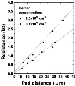
quently, the implanted samples were rapidly thermal an-nealed at 1100 °C for 60 s to repair the material damages induced by the implantation process. The annealed Be-implanted p-type samples show relatively higher carrier con-centrations of 2.6⫻1018cm⫺3–8.1⫻1019cm⫺3 than the as-grown p-type samples as measured by Hall measurement. Without any further annealing process after the contact met-allization, these samples show near perfect linear I – V char-acteristic as depicted in Fig. 4. Total resistance measured by CTLM is shown in Fig. 5. The specific contact resistance determined from the intercepts and slopes in the plots has a very low value of 4.5⫻10⫺6⍀ cm2 for the sample with a carrier concentration of 8.1⫻1019cm⫺3. This is a very low
ohmic contact resistance reported for p-type GaN. The effect of annealing on these Be-implanted samples was also inves-tigated. These samples were annealed under the same opti-mal annealing conditions as the nonimplanted as-grown p-type GaN samples described previously. The I – V curves of the annealed samples become nonlinear and the specific resistance also increased after annealing. We have not yet determined the exact cause of this. However, the reaction of Be atoms with O2may be one of the possible factors.
In summary, we reported the demonstration of low resis-tance ohmic contacts to p-type GaN samples using Ni/Pd/Au metallization scheme. For as-grown Mg-doped p-type GaN with low carrier concentration, we obtained a specific contact resistance as low as 1.0⫻10⫺4⍀ cm2 by annealing the samples in oxygen ambient at 550 °C for 5 min. For the Be-implanted p-type GaN samples, a lowest ohmic contact resistance value of 4.5⫻10⫺6⍀ cm2 was achieved without further annealing process. This Au-based Ni/Pd/Au metalli-zation contact should be suitable for making low resistance ohmic contact to either low carrier concentration
FIG. 1. Current–voltage (I – V) characteristics of Ni/Pd/Au contacts an-nealed in共a兲 air and 共b兲 nitrogen for different annealing temperatures.
FIG. 2. Current–voltage (I – V) characteristics of Ni/Pd/Au contacts an-nealed in oxygen for different annealing temperatures.
FIG. 3. Plot of the measured total resistance against the contact pad spacing for Ni/Pd/Au contacts annealed at 550 °C under different ambient condi-tions.
FIG. 4. Current–voltage (I – V) characteristics of Ni/Pd/Au contacts on Be-implanted p-type GaN.
3424 Appl. Phys. Lett., Vol. 77, No. 21, 20 November 2000 Chuet al.
This article is copyrighted as indicated in the article. Reuse of AIP content is subject to the terms at: http://scitation.aip.org/termsconditions. Downloaded to IP: 140.113.38.11 On: Thu, 01 May 2014 07:39:12
(1015– 1017cm⫺3兲 or high carrier concentration (⬎1018cm⫺3兲 p-type GaN.
This work was supported in part by the National Science Council of Republic of China共ROC兲 in Taiwan under Con-tract No. NSC89-2218-E-009-004 and by the Academic Ex-cellence Program of the Ministry of Education of ROC under the Contract No. 89-B-FA06-1-4-X89022. The authors would like to thank T. C. Wen of National Chiao Tung Uni-versity共NCTU兲 and Dr. C. I. Chiang of Chung Shan Institute of Science and Technology for providing the MOCVD grown GaN samples, and C. Y. Fang of NCTU for technical
assistance in the thermal annealing measurement. They would also like to thank Professor G. C. Chi of National Central University for using ion implantation facility.
1
S. Nakamura and G. Fasol, The Blue Laser Diode 共Springer, Berlin, 1997兲.
2S. Nakamura, M. Senoh, S. Nagahama, N. Iwasa, T. Yamada, T.
Mat-sushita, H. Kiyoku, Y. Sugimoto, T. Kozaki, H. Umemoto, M. Sano, and K. Chocho, Appl. Phys. Lett. 72, 2014共1998兲.
3M. A. Khan, A. R. Bhattarai, J. N. Kuznia, and D. T. Olson, Appl. Phys.
Lett. 63, 1214共1993兲.
4M. A. Khan, J. N. Kuznia, A. R. Bhattarai, and D. T. Olson, Appl. Phys.
Lett. 62, 1786共1993兲.
5
M. A. Khan, J. N. Kuznia, D. T. Olson, J. M. Van Hove, M. Blasin-game, and L. F. Reitz, Appl. Phys. Lett. 60, 2917共1993兲.
6J. S. Foresi and T. D. Moustakas, Appl. Phys. Lett. 62, 2859共1993兲. 7M. E. Lin, Z. Ma, F. Y. Huang, Z. F. Fan, L. H. Allen, and H. Morkoc,
Appl. Phys. Lett. 64, 1003共1994兲.
8Z. Fan, S. Mohammad, and W. Kim, Appl. Phys. Lett. 68, 1672共1996兲. 9T. Kim, M. C. Yoo, and T. Kim, Mater. Res. Soc. Symp. Proc. 449, 1061
共1997兲.
10J. K. Ho, C. S. Jong, C. C. Chiu, C. N. Huang, and K. K. Shih, Appl. Phys.
Lett. 74, 1275共1999兲.
11Y. Koide, T. Maeda, T. Kawakami, S. Fujita, T. Uemura, N. Shibata, and
M. Murakami, J. Electron. Mater. 28, 341共1999兲.
12A. K. Fung, J. E. Borton, M. I. Nathan, J. M. Van Hove, R. Hickman, P.
P. Chow, and A. M. Wowchak, J. Electron. Mater. 28, 572共1999兲.
13
J. K. Kim, J. L. Lee, J. W. Lee, H. E. Shin, Y. J. Park, and T. Kim, Appl. Phys. Lett. 73, 2953共1998兲.
14T. Kim, J. Khim, S. Chae, and T. Kim, Mater. Res. Soc. Symp. Proc. 468,
427共1997兲.
15
J. S. Jang, K. H. Park, H. K. Jang, H. G. Kim, and S. J. Park, J. Vac. Sci. Technol. B 16, 3105共1998兲.
16J. S. Jang, I.-S. Chang, H.-K. Kim, T.-Y. Seong, S. Lee, and S. J. Park,
Appl. Phys. Lett. 74, 70共1999兲.
17
L. Zhou, W. Lanford, A. T. Ping, I. Adesida, J. W. Yang and A. Khan, Appl. Phys. Lett. 76, 3451共2000兲.
FIG. 5. Plot of the measured total resistance against the contact pad spacing for Ni/Pd/Au contacts on Be-implanted p-type GaN.
3425
Appl. Phys. Lett., Vol. 77, No. 21, 20 November 2000 Chuet al.
This article is copyrighted as indicated in the article. Reuse of AIP content is subject to the terms at: http://scitation.aip.org/termsconditions. Downloaded to IP: 140.113.38.11 On: Thu, 01 May 2014 07:39:12