ELSEVIER Thin Solid Films 270 ( 1995) 531-536
Metal-organic
chemical vapor deposition of tantalum nitride barrier
layers for ULSI applications
M.H. Tsai a, S.C. Sun a, C.P. Lee a, H.T. Chiu b, C.E. Tsai b, S.H. Chuang b, S.C. Wuc
a Department of Electronics Engineering and Institute ofElectnmics. Natiorul Nano Device Laboratory, National Chiao Tung University,Hsinchu 30050,‘Tuiwun
h Institute of Applied Chemistry. Nationul Chiuo Tung University.Hsinchu 30050, Taiwun ’ Institute of Physics, National Tsing Hwn University, Hsinchu 30050, Taiwan
Abstract
Low-resistivity tantalum nitride (TaN) films were deposited by low-pressure metal-organic chemical vapor deposition (MOCVD) using a new precursor tertbutylimidotrisdiethylamidotantalum. The surface morphology and the step coverage of TaN films were characterized by scanning electron microscopy. The film deposited at 450°C had nearly 100% step coverage and the step coverage decreased to 25% for the films deposited at 650°C. The carbon and oxygen concentrations are about 10 at.% in the CVD TaN films, as determined by Auger electron spectroscopy. From Rutherford backscattering spectroscopy and secondary ion mass spectroscopy analysis, TaN films were found to be effective diffusion barriers between aluminum and silicon up to 550°C. The electrical measurements of diode-leakage current indicate that the Al/TaN/Si structure remained stable up to 5OO”C, after which Al started to diffuse through the TaN layer and resulted in a higher leakage current.
Keywords: Chemical vapour deposition; Organometallic vapour depositon; Metallization; Tantalum
1. Introduction
Aluminum has been widely used for contacts and inter- connections in both bipolar and metal-oxide-semiconductor integrated circuits (IC). Low-temperature interdiffusion of aluminum and silicon during contact sintering, passivation, or packaging of the device can result in a degradation of the shallow junction devices [ 11. Device reliability can be improved by interposing a barrier layer between Al and Si which prevents intermixing during further processing. Refractory metal nitrides are attractive candidates as diffusion barriers owing to their high conductivity, high thermal sta- bility and resistance to diffusion of foreign atoms [ 2,3]. Stoi- chiometric TIN has been extensively investigated for this application and has been shown to be effective as a barrier layer between Al and Si in the temperature range of 45& 550°C [ 4-61. More recently, thin films of WN, and TaN, have also been studied as diffusion barrier layers [ 7,8]. The TaN, has especially attracted great interests because of its high thermal stability, in contrast to WN, in which nitrogen will decompose at an annealing temperature higher than 800°C [7].
Previous studies of reactive sputtered TaN and Ta,N have reported that they were excellent metallurgical diffusion bar-
0040.6090/95/$09.50 0 1995 Elsevier Science S.A. All rights reserved SSDIOO40.6090( 95 )06752-3
riers between copper and Si [ 9, lo], and between aluminum and Si substrates [ 1 l-131. However, owing to the poor step coverage caused by the shadowing effect in the small feature size ( <0.35 km) and high aspect ratio contact and via, the reactive sputtering process may be reaching its limit of use- fulness. In this paper, we focus on the chemical vapor depo- sition (CVD) of TaN using a new metal-organic precursor, tertbutylimidotrisdiethylamidotantalum (TBTDET) . We performed Rutherford backscattering spectroscopy (RBS) and Auger electron spectroscopy (AES) experiments. The secondary ion mass spectroscopy (SIMS) and P+ /N diode electrical measurements were made in order to study the composition and diffusion barrier mechanism.
2. Experimental details
Phosphorus-doped ( 100) silicon substrates of 10-20 fi cm were prepared. The deposition of CVD-TaN films was carried out in a cold-wall low-pressure chemical vapor deposition (LPCVD) reactor. The base pressure was maintained at 1 X lops Torr by a diffusion pump. Liquid precursor TBTDET was contained in a glass vessel and heated to 3& 50°C. Prior to deposition, the substrate was first cleaned by
532 M.H. Tsui et ul. / Th Sold Fdnzs 270 (1995) 531-536
the standard RCA method. In order to remove the native oxide layer on the silicon surface, in-situ H2 and Ar sputtering was carried out in the LPCVD reactor by controlling the r.f. power density. TaN films were deposited at temperatures ranging from 450 to 650°C. Film thickness was measured by scanning electron microscopy (SEM). The resistivity was measured by a four-point probe. Impurity profiles were obtained from AES, X-ray photoelectron spectroscopy (XPS), and wave- length dispersive spectroscopy (WDS). RBS was used to study the interdiffusion behavior of the Al/TaN/Si structure using 2MeV He+ and a detector angle of 165”. The aluminum and silicon diffusion in the TaN layer was further analyzed by SIMS measurements using a Cameca IMS4F with an 0: ion beam at a 36” incident angle. The surface morphology was observed by SEM and atomic force microscopy (AFM) Cross-sectional SEM was employed to evaluate the step cov- erage of the films.
Pf
/N
junction diodes prepared for the electrical measure- ment of the barrier property were first implanted with BF,’ at 50 keV and 3 X lOI cm-‘. The samples were annealed at 900°C for 30 min in nitrogen. The junction depth of P+ layer was 0.3 pm. TaN barrier layers were subsequently deposited and exposed in the air before 250 nm pure Al was evaporated on top of TaN. The CVD-TaN was etched in a SF6 plasma after aluminum patterns were etched by the conventional wet etching solution. Samples were then thermally annealed at temperatures between 400 and 650°C for 30 min in vacuum. The leakage current was measured using HP4145B at - 5 V reverse bias for the thermal stability study.3. Results and discussion
Fig. 1 shows the dependence of the deposition rate on the source temperature. The typical deposition rate was about 1.5 nm mini at the source temperature of 40°C. The deposition rate can be raised by increasing the source temperature. For example, the deposition rate at a wafer temperature of 600°C was increased from 1.5 nm min-’ to 5.0 nm min-
’
as the source temperature was raised from 40°C to 50°C. The pre- cursor is thermally stable at room temperature. No source decomposition was observed up to 100°C.The surface morphology was evaluated as a function of deposition temperature. Films deposited at 450°C shown in
I Tsu,=600 OC 2 50
i40
4
; 3o
2 20 s g 10 & 0L
30 35 40 45 50 55Source Temperature (?I)
Fig. 1, Growth rate as a function of source temperature.
i ./ /
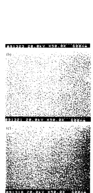
Fig. 2. SEM micrographs of TaN films deposited at (a) 45O”C, (b) 550°C. and (c) 650°C.
Fig. 2(a), appear very smooth with a surface roughness r.m.s value of 0.9 nm. The surface becomes rougher as the depo- sition temperature is increased. The increase in surface rough- ness is presumably due to the granular structure at higher deposition temperature. The grain size increases with depo- sition temperature. At 550°C (Fig. 2(b) ) the roughness r.m.s value is about 30 nm. The surface morphology of the films deposited at 650°C (Fig. 2(c)) is nearly the same as that deposited at 550°C.
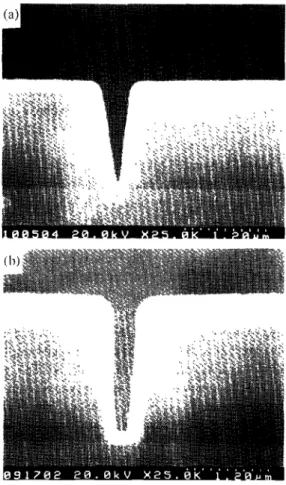
The step coverage was examined by depositing CVD TaN on a 0.8 km-width and 1.6 pm-deep trench. To obtain a quantitative measurement of film conformality, the step cov- erage is defined as film thickness on the trench bottom divided
M.H. T.sui et ul. /Thin Solid Fi/ms 270 (1995) 531-536 533
Fig. 3. Step coverage as a function of deposition temperature. Cross-sectional SEM micrographs of TaN films deposited at (a) 45O”C, (b) 550°C and Cc) 650°C.
by that at the wafer surface. Fig. 3(a), 3 (b), and 3(c) show the SEM micrographs of TaN films deposited over trenches at substrate temperaturesof450”C, 55O”C, and 650°C respec- tively. The film deposited at 450°C had a nearly 100% step coverage. No obvious grain boundary was found. As the substrate temperature was increased to 550°C the step cov- erage decreased to 60%. The films showed a grain boundary and two distinct structures for the films in the trench and on the wafer surface. The TaN films deposited on the wafer surface were of equiaxial structure and the TaN deposited in the trench showed a columnar structure. This may have resulted from the different deposition mechanisms that are involved in the films deposited at wafer surface and in the
trench. The TaN deposited in the trench may suffer a greater source depletion effect during the thermal pyrolysis process. At 650°C deposition, both the films at the wafer surface and in the trench showed a columnar structure. The step coverage decreased to 25%. Even at 25% step coverage, this film still demonstrated an excellent continuity around corner regions of the bottom of the contact, in contrast with the poor step coverage of the sputtered films. Poor conformality can be expected at high deposition temperatures, because of the high sticking coefficient [ 141. Operating the process at a temper- ature of 450°C does improve the conformality of the resulting films, but, as mentioned above, other film properties are degraded.
Fig. 4 shows the AES depth profiles of the tantalum nitride film deposited at 600°C. After the surface oxygen and carbon contamination was sputtered away, AES revealed 10 at.% carbon and 10 at.% oxygen in the films. The nitrogen con- centration was about 30 at.%, lower than the tantalum (50 at.%). However, the N/Ta ratios determined by RBS show that the films were nitrogen rich with N/Ta ratios of 1. l-l .3. This may have resulted from the preferred sputtering of the light element during depth profiling [ 151.
To examine the correlation between the deposition tem- perature and the stoichiometry of the TaN films, WDS was performed on the TaN films deposited at various tempera- tures. Based on the data from WDS, N/Ta, C/Ta, and O/Ta ratios are plotted against the deposition temperature as shown in Fig. 5. The N/Ta, C/Ta, and O/Ta ratios are about 1.4, 0.7, and 0.2 for the films deposited at 450°C. Such high nitrogen and carbon concentrations may have resulted from the incomplete thermal decomposition of the precursor.
u
OoV
15Sputter Time (min.)
Fig. 4. Auger depth profiles of the TaN film deposited at 600°C
1.5 1.0 m s 0.5 0.0 400 450 500 550 600 650 700 Temperature (“C)
Fig. 5. N/Ta, C/Ta, and O/Ta ratios of the TaN films as a function of deposition temperature.
534 50 g 40 B g 30 .9 Jj 20 z TJ 10 8 U 0 0.0 0.2 0.4 0.6 0.8 1.0 Contact size (bm)
Fig. 6. Calculated total contact resistance as a function of contact size for the AI/TaN/TiSi,/Si contact structure with TaN resistivity as a parameter.
Increasing the deposition temperature above 550°C produces near unity N/Ta ratio films. Strong Ta = N double bonds in the TBTDET were suggested to have preserved the “TaN” portion of the precursor into the lattice of cubic TaN in the high-temperature pyrolysis process. O/Ta ratio was almost independent of the deposition temperature, except at 650°C at which the oxygen concentration showed a slight increase. This is presumably due to the open paths in columnar grain boundary of the films which are easily penetrated by oxygen. The resistivity is an important consideration for the barrier metal in IC applications. High resistivity will cause a high contact resistance. To investigate the impact of film resistivity on the overall contact resistance, an Al/TaN/TiSi,/Si con- tact structure is used in our calculation. The contact resistance of titanium silicide and PC silicon is assumed to be 1 X 10e8 R cm-‘. A 60-nm thick CVD TaN barrier layer is confor- mally deposited in a cylindrical contact hole of 1 km-deep, and the contact hole is completely filled with Al which has a specific resistivity of 3 p_L! cm. The calculated total resistance as a function of contact size for the Al/TaN/TiSi,/Si contact structure is shown in Fig. 6. For contact sizes greater than 0.5 km, the effect of barrier metal resistivity on the contact resis- tance is insignificant. The resistivity requirement becomes more stringent as the contact size shrinks. The barrier layer having a resistivity higher than 1000 ~0 cm will hinder its usefulness for a contact size smaller than 0.35 pm. Based on the experimental results, the resistivity of the TaN films deposited at temperatures below 550°C was higher than 5000 p_fi cm. This film is not suitable for the barrier metal appli- cation. Higher deposition temperatures will reduce the resis- tivity of the TaN films. Films deposited at 650°C have a resistivity of 900 pfi cm. This film is a useful barrier metal for contact sizes as small as 0.3 pm.
It has been suggested that the decomposition of TaN and the subsequent formation of Al,Ta and AlN are responsible for the failure of TaN as a diffusion barrier [ 33. Fig. 7 com- pares the sheet resistance of Al/CVD-TaN/Si and Al/PVD- TiN/Si multilayer structures annealed under various temperatures in vacuum for 30 minutes. Since the resistance of the Al film is much lower than the resistance of the under- lying barrier and contact layers, an increase in resistance is directly related to the consumption of Al by the underlying layer. The sheet resistances of both Al/CVD-TaN/Si and
Al/PVD-TiN/Si structures were stable up to 525°C. The stable value of sheet resistance indicates that the aluminum tilm in the Al/barrier/Si structure remains intact up to 525°C. Above 525”C, the sheet resistance began to increase for both CVD-TaN and PVD-TIN barriers. This increase in sheet resistance is an indication that Al films were consumed either by reaction with TaN (or TIN) or by diffusion into the barrier layer. Since there is no detectable amount of aluminum dif- fusion into the barriers at this annealing temperature as deter- mined by RBS and SIMS analysis, it is expected that the aluminum was mainly consumed by the aluminides (Al,Ta or Al,Ti) formation. Moreover, the increase in resistance at 550°C is more significant in the PVD-TIN structure than CVD-TaN, which may imply a more severe reaction between Al and TIN in the PVD-TIN barrier structure.
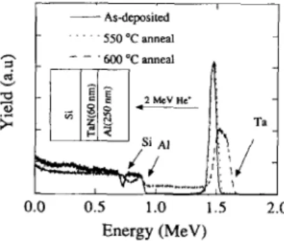
Fig. 8 shows the RBS spectra of the Al/TaN/Si structure as-deposited and after annealing at 550°C and 600°C. The RBS spectrum for the 550°C annealed sample has a nearly complete overlap with that of the as-deposited sample. Only a small amount of tantalum migration in the Al/TaN interface was found. The tantalum migration into the aluminum film was presumably due to the Al,Ta formation. The interface of the TaN and Si remains a sharp contrast and no tantalum diffusion to the silicon was found. Raising the annealing temperature to 600°C results in broad and weak RBS peak, which indicate the occurrence of intermixing of Ta, Al, and Si. Above 600°C annealing, the top layer aluminum, observed by SEM, formed irregular bumps. This will interfere with the accuracy of RBS analysis.
9
.2/
3
5
500/
8
0,..:
300 400 500 600 700 Temperature (“C)Fig. 7. Sheet resistance of Al/CVD-TaN/Si and AI/PVD-TiN/Si multilayer structures as a function of anneal temperature (30 min in vacuum).
_ As-deposited
0.0 0.5 1.0 1.5 2.0
Energy (MeV)
Fig. 8. RBS spectra of the AI/TaN/Si structure as-deposited, after 550°C and 600°C annealing.
M.H. Tsai et al. /Thin Solid Films 270 (1995) 531-536 535 0 0.2 0.4 0.6 0.8 Depth (w) __ 0 0.2 0.4 0.6 0.8 Depth (pm) 600 “C annealin 0 0.2 0.4 0.6 0.8
Fig. 9. SIMS depth profiles of the Al/CVD-TaN/Si structure after (a) 5OO”C, (b) 55O”C, and (c) 600°C annealing.
SIMS analysis may have a higher sensitivity than RBS in detecting the metal diffusion in silicon. Lane et al. [ 161 have studied W and Ta as diffusion barriers against copper diffu- sion using RBS and SIMS. Their results showed that although no sign of interdiffusion was found by RBS, SIMS had already detected the copper diffusion into the Si with a con- centration of about 2 X 10” cm-3. In order to have a better understanding of the failure mechanism of the CVD-TaN as barrier layers, SIMS measurement was conducted for the Al/ TaN/Si layered structure after various annealing treatments. Fig. 9(a) shows the SIMS depth profiles of the layered struc- ture after annealing at 500°C. There may be some Al,Ta formation, but a very small amount of Ta outdiffusion into Al. Increasing the annealing temperature to 550°C (Fig. 9(b) ) will cause more tantalum outdiffusion in Al and more Al,Ta formation. The Ta and Si interfaceremains unchanged. Al started to diffuse further in the TaN film, but remained inside the TaN layer. After 600°C annealing, as shown in Fig. 9(c), the aluminum diffused deeply into the silicon substrate with a long tail of tantalum diffusion in silicon as well.
Fig. 10 represents the leakage current distribution of a Al(250 nm) /TaN(GO nm)/Si Pf
/N
diode structure after 45O”C, 500°C and 550°C annealing for 30 min. The currentlo-‘0 10-g 10-a lo” lod lo-5 lod
Leakage Current (Akrr?)
2 80 AI/l’aN(6Onm)/Si “,m 0 &j 40 $ rf: 20
lo-‘0 10’9 10-6 10’7 lo4 10” lOA Leakage Current (A/cm*)
0
l@‘O KY9 10-g 10-7 106 lo” lo4 Leakage Current (A/cm*)
Fig. 10. Pf /N diode leakage current density distribution of the AUCVD- TaN/Si structure after annealing at (a) 450°C (b) 500°C. and (c) 550°C.
distribution did not change up to 500°C. At 550°C the meas- ured diode leakage showed a wide distribution with a signif- icant portion of leakage higher than lo-” A cm ‘. Although there is no measurable amount of aluminum diffusion in the silicon substrate from SIMS analysis, the electrical measure- ments demonstrate that the diode has degraded at 550°C. As mentioned in the previous paragraph, the failure temperature of TaN barrier from SIMS data is about 600°C. The apparent difference in failure temperature between diode leakage measurement and SIMS data is perhaps due to the aluminum diffusion around the weak spot of TaN or along the grain boundary of columnar structure of TaN into the silicon sub- strates that are not easily detected by the SIMS measurements.
4. Conclusions
In summary, low-resistivity TaN films were deposited by the LP-MOCVD method using a new precursor, TBTDET. Stoichiometric TaN films were obtained at temperatures higher than 550°C. The 60-nm TaN film was proved to be an effective barrier against aluminum diffusion up to 500°C. Increasing the sintering temperature to 550°C caused the TaN barrier to start to deteriorate by aluminide formation and the aluminum diffusion along the grain boundary of the columnar structure in the TaN barrier layer.
536 M.H. Tsui et ul. /Thin Solid Films 270 (1995) 531-536 Acknowledgements
This work is supported by the National Science Council of the Republic of China under the contract NSC84-2215-E009- 025 and an industrial grant from United Microelectronics Corporation.
References
[ 1 ] J.O. McCalin and H. Sankur, Appl. Phys. Lett., 22 ( 1975) 64. [2] M.-A. Nicolet, Thin Solid Films, 52 (1978) 415.
[3] M. Wittmer, J. Vuc. Sci. Technol. A, 2 ( 1984) 273. [4] C.Y. Ting and W. Wittmer, Thin Solid Films, 96 (1982) 327. [5] A. Armigliato and G. Valdre, J. Appl. Phys., 61 (1986) 390. [6] A. Kohlhase, M. Mandl and W. Palmer, J. Appl. Phys., 65 ( 1989)
2464.
171 X. Sun, E. Kolawa, J.-S. Chen, J.S. Reid and M.-A. Nicolet. Thirl Solid Films, 236 (1993) 347.
[8] F.C.T. So, E. Kolawa. X.-A. Zhao, E.T.S. Pan and M.-A. Nicolet, J. Appl. Phys.. 64 (1988) 2787.
[9] K. Holloway, P.M. Fryer, C. Cabral, J.M.E. Harper, P.J. Bailey and K.H. Kelleher, J. Appl. Phys., 71 (1992) 5433.
[ 101 J.O. Olowolafe, C.J. Mogab, R.B. Greygory and M. Kottke, J. Appl. Phys., 72 ( 1992) 4099.
[ 11 I K. Sasaki, A. Noya and T. Umezawa, Jpn. J. Appl. Phys., 29 ( 1990) 1043.
[ 121 B. Mehrotra and J. Stimmell, J. Vat. Sci. Technol. B, 5 ( 1987) 1736. [ 131 M.A. Faroo, S.P. Muraka, C.C. Chang and F.A. Baiocchi, J. Appl.
Phys., 70 (1991) 1369.
[ 141 T.S. Cale, M.B. Chaara, G.B. Raupp and I.J. Raaijmakers, Thin Solid Films. 236 (1993) 294.
[ 151 S. Ingrey, M.B. Johnson and R.W. Streater, J. Var. Sci. Technol.. 20 (1982) 968.
[ 161 L.C. Lane, T.C. Nason. G.-R. Yang, T.-M. Lu and H. Bakhru, J. Appl. Phys., 69 (1991) 6719.