Novel Two-Bit HfO
2
Nanocrystal Nonvolatile
Flash Memory
Yu-Hsien Lin, Student Member, IEEE, Chao-Hsin Chien, Associate Member, IEEE, Ching-Tzung Lin,
Chun-Yen Chang, Life Fellow, IEEE, and Tan-Fu Lei, Member, IEEE
Abstract—This paper presents a novel nonvolatile
poly-Si-oxide–nitride–oxide–silicon-type Flash memory that was fabri-cated using hafnium oxide (HfO2) nanocrystals as the trapping
storage layer. The formation of HfO2nanocrystals was confirmed
using a number of physical analytical techniques, including ener-gy-dispersive spectroscopy and X-ray photoelectron spectroscopy. These newly developed HfO2 nanocrystal memory cells exhibit
very little lateral or vertical stored charge migration after 10 k program/erase (P/E) cycles. According to the temperature-acti-vated Arrhenius model, we estimate that the activation energy lies within the range 2.1–3.3 eV. These HfO2 nanocrystal memories
exhibit excellent data retention, endurance, and good reliability, even for the cells subjected to 10 k P/E cycles. These features suggest that such cells are very useful for high-density two-bit nonvolatile Flash memory applications.
Index Terms—Flash memory, hafnium oxide (HfO2),
nanocrys-tals, nonvolatile memories.
I. INTRODUCTION
P
OLY-Si-OXIDE–NITRIDE–OXIDE–SILICON (SONOS)-type structure memories, which include nitride and nano-crystal memories, have recently attracted much attention for their application in the next-generation nonvolatile memories [1]–[10]. They exhibit many advantages, e.g., easy to fabricate, high program/erase (P/E) speed, low programming voltage and power consumption, and better potential for scalability below the 70-nm node, according to the International Technology Roadmap for Semiconductors (ITRS) [11]. Unfortunately, many concerns still remain for this type of memories. For con-ventional SONOS memory, erase saturation and vertical stored charge migration [7], [8] are two major drawbacks, whereas for nanocrystal memories, the most challenging tasks are how to maintain acceptable charge capability of the discrete storage nodes and fabricate nanocrystals with constant size, high density, and uniform distributions [9]. In recent years, various ONO processing technology [10] and alternative trapping layer material [12] have been investigated to improve the cell data retention. For example, the use of an Al2O3trapping layer and HfAlO3 to replace Si3N4 has been considered because their material bandgaps and high trap densities provide superior P/E speed and data retention [12], [13]. Moreover, various kindsManuscript received October 31, 2005; revised January 10, 2006. This work was supported by the National Science Council of Taiwan, R.O.C., under Contract 942215E009070. The review of this paper was arranged by Editor R. Shrivastava.
The authors are with the Department of Electronics Engineering and the Institute of Electronics, National Chiao-Tung University, Hsinchu 300, Taiwan, R.O.C. (e-mail: [email protected]).
Digital Object Identifier 10.1109/TED.2006.871190
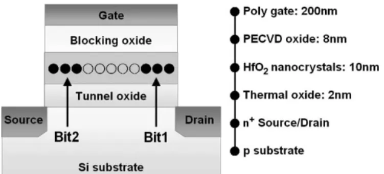
Fig. 1. Schematic representation of the HfO2nanocrystal Flash memory cell
structure and localized charge storage.
of nanocrystals, such as silicon (Si), germanium (Ge), and metal nanocrystals, may be used to provide charge storage for nonvolatile memories [1]–[6].
In this paper, we propose a novel technique that is fully com-patible with the current CMOS technologies in forming very localized HfO2 nanocrystals for application in high-density two-bit nonvolatile Flash memory. This approach utilizes spin-odal decomposition of hafnium silicate after rapid thermal annealing (RTA) treatment at a sufficiently high temperature [14], [15]. Using this technique, we can readily isolate the HfO2 nanocrystals from each other within an SiO2-rich matrix. With a large bandgap offset between HfO2 and SiO2, memory cell using HfO2 nanocrystal may exhibit superior characteristics, such as a larger memory window, high P/E speeds, long reten-tion time, excellent endurance [16], [17], and strong immunity against disturbance. In addition, by comparing to those pub-lished ones using Si, Ge, and metal nanocrystals [1]–[6], our HfO2 nanocrystal memory possesses many advantages, such as larger memory window and better data retention. Moreover, high-temperature process for the source/drain (S/D) activation is no longer detrimental because this step can help further stabilize the HfO2 nanocrystal; however, it will oxidize the other nanocrystals and lead to a decrease in memory window. The process is very simple, reproducible, and reliable, with less metal contamination concern.
II. DEVICEFABRICATION
An example of the fabrication process of the HfO2 nanocrys-tal memory devices is demonstrated by a local oxidation of silicon (LOCOS) isolation process on a p-type, 5- to 10-Ω· cm, (100) 150-mm silicon substrate (Fig. 1). First, a 2-nm tunnel oxide was thermally grown at 1000 ◦C in a vertical furnace
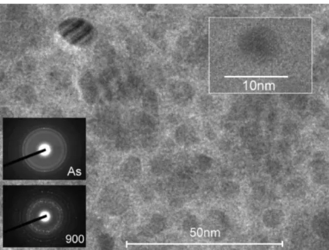
Fig. 2. Planar-view HRTEM image of the HfO2nanocrystals. The cell size
is 5–8 nm, and the dot density is 0.9−1.9 × 1012cm−2. The inset shows the
diffraction patterns of the as-deposited and 900◦C RTA-treated samples.
system. Next, a 12-nm amorphous HfSiOxsilicate layer was
de-posited by cosputtering with pure silicon (99.9999% pure) and pure hafnium (99.9% pure) targets in an oxygen gas ambient. The cosputtering process was performed with 7.6× 10⁻³Torr at room temperature (RT) and with precursors of O2[3 standard cubic centimeters per minute (sccm)] and Ar (24 sccm); in which both direct current (dc) sputter powers were set at 150 W. The samples were then subjected to RTA treatment in an O2ambient at 900◦C for 1 min to convert the HfSiOxsilicate
film into the separated HfO2and SiO2phases. Their composi-tions were identified using both energy-dispersive spectroscopy (EDS) and X-ray photoelectron spectroscopy (XPS). An 8-nm blocking oxide was then deposited through high-density plasma chemical vapor deposition (HDPCVD), followed by an N2 densification process at 900◦C for 1 min. Subsequently, poly-Si deposition, gate patterning, S/D implanting, and the remaining standard CMOS procedures were completed to fabricate the HfO2nanocrystal memory devices.
Fig. 2 shows planar-view high-resolution transmission mi-croscopy (HRTEM) image of the HfO2 nanocrystals. The average nanocrystal size was 5–8 nm; the density was as high as 0.9−1.9 × 1012 cm−2. Clearly, the nanocrystals were well separated in two dimensions within the SiO2, in which the average distance is > 5 nm. This isolation of the nanocrystals prevents the formation of effective conductive paths between adjacent nodes. The mechanism responsible for the formation of HfO2nanocrystal is through the phase separation of hafnium silicate into a crystallized structure [14]. For the Hf-silicate layer, the compositions within metastable extensions of the spinodal are unstable, and HfO2nanocrystal will be formed and wrapped up by SiO2after cooling down from RTA processing. In addition, it is clear from the diffraction patterns that the as-deposited film was amorphous and that the sample subjected to RTA was polycrystalline. The HfO2nanocrystals have mon-oclinic crystalline structures. Table I lists the original average concentrations of the individual elements in the as-deposited amorphous HfSiOx silicate layer, as determined through EDS
analysis at a spatial resolution less than 2.0 nm. We observe that the as-deposited HfSiOx layer comprised ca. 40 mol% HfO2
and 60 mol% SiO2; the average elemental concentrations of Hf, Si, and O were 12.61%, 18.99%, and 68.40%, respectively. At this elemental composition, we can readily reproduce high-density HfO2 nanocrystal dots embodied within an SiO2-rich matrix after RTA in an O2ambient.
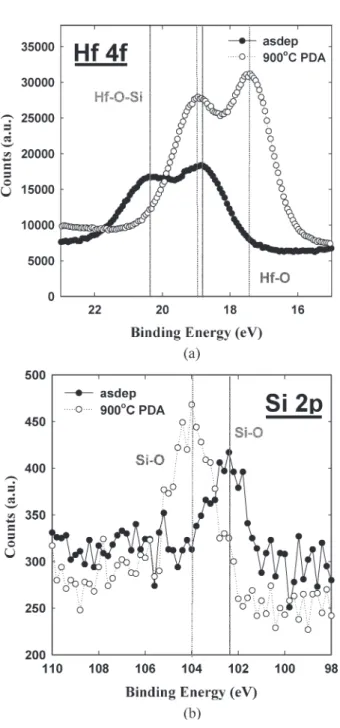
We have also performed XPS measurements using an Al Kα X-ray source (1486.6-eV photons) to determine the bonding environments of the Hf and Si atoms. Fig. 3(a) shows the Hf 4f photoemission peaks of the as-deposited Hf-silicate film before and after its postdeposition annealing (PDA) at 900 ◦C under O2. In the as-deposited film, we observe well-defined 4f5/2and 4f7/2 feature peaks that correspond to Hf–O–Si bonding. We confirmed that HfO2nanocrystals formed after RTA through the observed shifts of these peaks to lower binding energies (4f5/2: ca. 18.9 eV; 4f7/2: ca. 17.4 eV) [18], [19]. Fig. 3(b) shows Si 2p XPS spectra of the as-deposited Hf-silicate film before and after RTA. Again, the Si–O bonds in SiO2 network (104 eV) are prominent; their peak intensity increased after PDA. These results provide definite evidence for phase separation occurring in the PDA-treated Hf-silicate film.
For the cell operation, channel hot-electron injection and band-to-band hot-hole injection for the programming and eras-ing, respectively, have been used. All cells described in this pa-per have dimensions of length/width (L/W ) = 1/2 µm. Fig. 4 demonstrates the feasibility of performing two-bit operation with our HfO2 nanocrystal memories through a reverse-read scheme in a single cell. From the Ids−Vgs curves, it is clear that we could employ forward and reverse reads to detect the in-formation stored in the programmed bit1 and bit2, respectively. The read operation was achieved using a reverse-read scheme. Table II summarizes the bias conditions for two-bit operation.
III. RESULTS ANDDISCUSSION
A. Migration of Storage Charges
One of the major advantages that HfO2 nanocrystal Flash memory has over floating-gate flash erasable programmable read-only memory (EEPROM) is its better data retention, which is attributed to its excellent capability of locally trapping charges with no significant lateral or vertical migration. We can measure the degrees of migration from the cells after the cycling. One method for characterizing the lateral extent of the trapped electrons is to monitor the variation of the threshold voltage Vt for a programmed memory cell in the presence
of a changing drain current Vd [19]. Fig. 5 shows a plot of
Fig. 3. XPS spectra of the as-deposited and 900◦C RTA-treated samples. (a) Hf 4f. (b) Si 2p. These spectra indicate that the Hf-silicate was fully converted to HfO2 and SiO2through phase separation after PDA at 900◦C
under O2.
temperature in a programmed cell after 10 k P/E cycling. Here,
Vt is defined as the applied gate voltage at which the drain
current is 1 µA. Inasmuch as channel hot-electron injection is used for the cell programming, the trapped electrons in the HfO2 nanocrystal trapping layer are more likely to be located near the n+ drain junction. These trapped electrons will raise the potential barrier near the drain side and increase the value of Vt. The degree of the Vtshift is believed to be proportional
to the trapped electron density if the drain terminal is main-tained at a relatively low potential (e.g., Vd = 0.1 V). When
a sufficiently high drain bias (e.g., Vd= 1.5 V) is applied,
however, the drain depletion region will be extended toward the channel and, consequently, block the influence from the trapped electrons for the measured Id−Vgcharacteristics [20].
Fig. 4. Ids−Vgscurves of the two-bit memory in a cell; forward read and
reverse read for programmed bit1 and programmed bit2. TABLE II
OPERATIONPRINCIPLES ANDBIASCONDITIONSUTILIZEDDURING THE
OPERATION OF THEHfO2NANOCRYSTALFLASHMEMORYCELL
Fig. 5. Vertical charge migration characteristics of the HfO2 nanocrystal
Flash memory cells after 10 k P/E cycling.
Therefore, this proposed technique can detect the lateral profile of the trapped electrons. To enhance the storage charge move-ment in the HfO2nanocrystal trapping layer, the programmed samples were subjected to high-temperature baking at 80 ◦C and 125◦C for 2000 s, respectively. Remarkably, the Vt−Vd curves for the cycled device and the baked devices exhibit very little difference, suggesting that lateral migration of the storage charges in the HfO2nanocrystal trapping layer is rather
Fig. 6. Lateral charge migration characteristics of the HfO2nanocrystal Flash
memory cells after 10 k P/E cycling.
Fig. 7. Activation energy characteristics of the HfO2nanocrystal Flash
mem-ory cells taken from five samples.
insignificant. It was attributed to the effective isolation of each nanocrystal within the SiO2 matrix. Next, we investigated the influence of the vertical field on charge retention, i.e., vertical migration. Fig. 6 shows the Vtvariation over time for various
stress conditions for the 10 k P/E cycled cells. Visible charge loss was observed when the applied gate voltage and temper-ature were raised up to−5 V and 125◦C. We thought that al-though the trap energy level in the nanocrystal is quite deep, the generated defects and interface traps of the 2-nm tunnel oxide after 10 k P/E cycled stress will help stored charges escape via trap-assisted tunneling. Therefore, vertical charge migration is more observable than lateral charge migration in our memory cell. We also calculated the activation energy for the traps of the HfO2 nanocrystals in the new cells (Fig. 7). Activation energy tracing is used widely to characterize the Arrhenius relation extracted from the temperature dependence of charge loss from nonvolatile memory as a function of time. For a given charge loss threshold criterion (in our case, 20% is used), the failure rates obtained at high temperature (125◦C–200◦C) can then be extrapolated to the nominal operating conditions. The model is based on a classical temperature-activated Arrhenius law, expressed in the form tR= t0× eEa/kT, where t0 is the retention time corresponding to an infinite temperature,
Ea is the activation energy, T is the temperature, and k is
the Boltzmann constant [21]. The activation energy, which is determined from the slopes of five samples, lies in the range
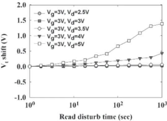
Fig. 8. Read disturbance characteristics of the HfO2 nanocrystal memory
devices. No significant Vt shift occurred for Vd< 4, even after 1000 s
at 25◦C.
Fig. 9. Drain disturbance characteristics of the HfO2 nanocrystal memory
cells. After 1000 s at 25◦C, only a 0.3-V drain disturb margin was observed.
2.1–3.3 eV, Obviously, it is higher than those values previously reported for conventional SONOS memories [22]–[24].
B. Disturbance
Fig. 8 demonstrates the read-disturbance-induced erase-state threshold voltage instability in a localized HfO2 nanocrystal trapping storage Flash memory cell under several operation conditions. For a two-bit operation, the applied bitline voltage in a reverse-read scheme must be sufficiently large (> 1.5 V) to be able to “read through” the trapped charge in the neighboring bit. The read-disturb effect is the result of two factors: the word line and the bit line. The word-line voltage during read may enhance RT drift in the neighboring bit [25]. On the other hand, a relatively large read bit-line voltage may cause unwanted channel hot-electron injection and, subsequently, result in a significant threshold voltage shift of the neighboring bit. In our measurements, the gate and drain biases were applied and the source was grounded. The results demonstrate clearly that almost no read disturbance occurred in our HfO2 nanocrystal Flash memory under low-voltage reading (Vg= 3 V; Vd=
2.5 V). For a larger memory window, we found that only a small read disturbance (ca. 0.3 V) can be observed after operation at
Vd= 4 V after 1000 s at 25◦C.
Fig. 9 shows the programming drain disturbance of our HfO2nanocrystal Flash memory. Two different drain voltages (Vd= 5 and 9 V) were applied in the programming drain
disturbance measurements at two different temperatures (T = 25◦C and 125◦C). We observed that a sufficient programming
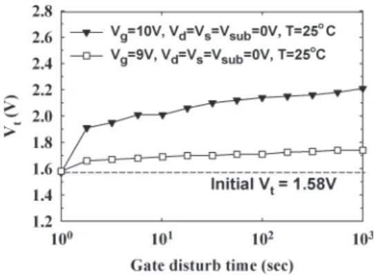
Fig. 10. Gate disturbance characteristics of the HfO2 nanocrystal memory
devices. A threshold voltage shift of only 0.22 V occurred after stressing at
Vg= 9 V and Vs= Vd= Vsub= 0 V for 1000 s.
drain disturb margin exists (∆Vt< 0.4 V), even after
program-ming at a value of Vd of 9 V under high temperature (T =
125◦C) and after stressing for 1000 s. Fig. 10 shows the gate disturbance characteristics in the erasing state. Gate disturbance may occur during programming for the cells sharing a common word line while one of the cells is being programmed. We observed a threshold voltage shift of only 0.16 V, i.e., negligible disturbance, under the following conditions: Vg= 9 V; Vs= Vd = Vsub= 0 V; stressed for 1000 s. It is interesting to know why this memory can exhibit such excellent gate disturbance characteristics with such a thin tunnel oxide; a nonnegligible current will be present in the tunnel oxide when a voltage of 9 V is applied to the gate electrode. Using a serial capacitor voltage divider model, we estimated that the voltage drop at the tunnel oxide would be 0.98 V if the trapping layer is assumed to be an HfO2film rather than a nanocrystal. Although a 0.98-V drop will cause a significant leakage current through an individ-ual 2-nm oxide layer, the data retention in the memory cell is related not only to the direct tunneling leakage current induced by such a voltage but also to the total tunneling situation in the whole gate stack, i.e., the effect that the potential barrier presented by the high-k material has on the tunneling current must be taken into account. In other words, it is incorrect to state that a large direct tunneling current will definitely exist in the interfacial layer and, in turn, that it will induce significant disturbance during programming.
C. Charge Pumping Characteristics
The charge pumping (CP) measurement was used to investi-gate the characteristics of our HfO2nanocrystal Flash memory. We used a trapezoidal gate pulse having a fixed pulse amplitude with varying Vgbl. The substrate current (the so-called “charge pumping current,” Icp) as a function of Vgblwas measured. The gate pulse have a frequency of 1 MHz and a 50% duty cycle; the rising and falling times were both 2 ns. Fig. 11 shows plots of the program-state charge pumping current Icpversus Vgbl for our HfO2 nanocrystal memory cell. Fowler–Nordheim (F–N) tunneling was used to program the cell with Vtlevels from 2.06
to 3.51 V. The open symbols represent the measured data. The program-state Icp curve shifted increasingly toward the right upon increasing the value of Vt as a result of an increase in
the amount of injected charge in the HfO2nanocrystal trapping
Fig. 11. Plots of Icpversus Vgblfor the HfO2nanocrystal memory cell after
F–N programming to different Vtlevels.
layer. Interestingly, a hump appeared in the left-hand edge of the curve in compliance with this shift. We decompose the resultant Icpcurve mathematically into two individual curves, i.e., A and B, in a fresh memory cell. We speculate that these two Icp curves arise from interlacing of the SiO2 matrix and HfO2 nanocrystals within the trapping layer. In other words, the memory is composed of two kinds of devices that have different gate dielectric configurations. The extracted threshold voltage in curve A is larger than that in curve B, even for a fresh memory, because the value of equivalent oxide thickness (EOT) of the gate stack in the region containing SiO2matrix is larger than that in the part containing the HfO2 nanocrystals. We believe that curve A is related to the SiO2matrix, and curve B corresponds to the HfO2 nanocrystals. With programming, it is clear that the Icp curve arising from the region containing the SiO2 matrix undergoes almost no shift, and the resultant distortion appearing in the measured Icpcurve is caused mainly by the charging of the HfO2 nanocrystal. This result implies that the programming charge was stored almost entirely within or around the HfO2nanocrystal rather than in the SiO2matrix. To confirm this hypothesis, we traced the measured curve by adding curve A to a horizontally shifted curve B; this approach works quite well. In addition, we also analyzed the devices formed from a pure HfO2 trapping layer on top of an SiO2 tunnel oxide structure. It was observed that only curve B shifted horizontally when programming (data not shown). Con-sequently, we conclude that HfO2nanocrystals can behave as an excellent local charge trapping centers.
D. Characteristics After P/E Cycling
Fig. 12 shows the endurance characteristics of the HfO2 nanocrystal memory cell. The programming and erasing con-ditions were Vg= Vd= 9 V for 10 µs and Vg=−5 V, Vd=
10 V for 1 ms, respectively. Remarkably, the values of Vt in
the program and erase states did not increase significantly up to 105 P/E cycles, whereas the memory window underwent a significant narrowing after 106 cyclic operations. The spatial distributions for electron and holes are localized during the channel hot-electron injection and band-to-band hot-hole in-jection for the programming and erasing, respectively, of our HfO2 nanocrystal memory. If the electron distribution does
Fig. 12. Endurance characteristics of the HfO2 nanocrystal memory after
10 k P/E cycling.
Fig. 13. Retention characteristics of the HfO2 nanocrystal memory after
10 k P/E cycling at 25◦C and 125◦C. No significant charge loss occurred at 25◦C, and only a very low charge loss occurred at 125◦C.
not completely match that for the hole, then each P/E cycle will leave a few electrons in the trapping layer [26]. This so-called “hard-to-erase” phenomenon cannot be eliminated readily when using band-to-band hot-hole erasing. Obviously, this is not an issue for our memory because the enhanced local electric field across the thin tunnel oxide in the region just beneath the nanocrystals can help in the injection of holes. Fig. 13 illustrates the retention characteristics of the HfO2 nanocrystal memory devices for a 10 k P/E stressed HfO2 nanocrystal memory cell both at RT (T = 25 ◦C) and above (T = 125◦C). Relative to the fresh device, the device operated at RT retained its good retention time (up to 105 s) for 10% charge loss [16]. We ascribe this result to the combined effects of the tight embrace of the HfO2 nanocrystals by the SiO2 -rich matrix and the sufficiently deep trap energy level of our memories (extracted activation energy: 2.1–3.3 eV). Therefore, despite the tunnel oxide having a thickness as low as 2 nm, no significant lateral or vertical charge migration occurred; as a result, the device displays superior retention characteristics for charge storage. At the temperature at 125◦C, we observed a more significant charge loss during the program state. This strong temperature dependence was predictable from the large activation energy, but the detailed mechanism remains under further investigation. Table III presents a comparison of our results with those of recent investigations into new devices [2], [5], [8]. Our system shows a number of salient features. First, our HfO2 nanocrystal memories exhibit larger memory
windows than do the other systems because of the large trap density of the high-k dielectric materials. Second, with respect to the P/E speed, we obtained a high speed of operation because we used channel hot-electron programming and band-to-band hot-hole erasing. Finally, we observed good retention with no vertical or lateral migration as a result of the HfO2na nocrystals being isolated effectively within the SiO2matrix.
IV. CONCLUSION
In this paper, we propose a novel, simple, reproducible, and reliable technique for the design of high-density HfO2 nanocrystals through the spinodal decomposition of hafnium silicate. Our nanocrystal memory exhibits superior characteris-tics in terms of negligible lateral or vertical migration of stored charge and good disturbance characteristics. The cells after 10 k P/E cycling also show a long retention time and excellent endurance. With this superior performance, we believe that HfO2nanocrystal Flash memory is quite suitable for the two-bit operation and that it has great potential for replacing the ONO stack in conventional SONOS-type Flash memories.
ACKNOWLEDGMENT
The authors would like to thank Dr. R. Klauser, Dr. C.-H. Chen, and Mr. S.-C. Wang at the National Synchrotron Ra-diation Research Center for their help with XPS analyses, Dr. C.-C. Leu and S.-L. Hsu at the National Nano Device Laboratory for their assistance during material analyses, and Prof. T. Wang and Prof. S. Chung for discussion on the electri-cal characteristics in this paper.
REFERENCES
[1] R. Ohba, N. Sugiyama, K. Uchida, J. Koga, and A. Toriumi, “Nonvolatile Si quantum memory with self-aligned doubly-stacked dots,” IEEE Trans.
Electron Devices, vol. 49, no. 8, pp. 1392–1398, Aug. 2002.
[2] R. Muralidhar, R. F. Steimle, M. Sadd, R. Rao, C. T. Swift, E. J. Prinz, J. Yater, L. Grieve, K. Harber, B. Hradsky, S. Straub, B. Acred,
W. Paulson, W. Chen, L. Parker, S. G. H. Anderson, M. Rossow, T. Merchant, M. Paransky, T. Huynh, D. Hadad, K.-M. Chang, and B. E. White, Jr., “A 6 V embedded 90 nm silicon nanocrystal nonvolatile memory,” in IEDM Tech. Dig., 2003, pp. 601–605.
[3] T. Baron, B. Pellissier, L. Perniola, F. Mazen, J. M. Hartmann, and G. Polland, “Chemical vapor deposition of Ge nanocrystals on SiO2,”
Appl. Phys. Lett., vol. 83, no. 7, pp. 1444–1446, Aug. 2003.
[4] Q. Wan, C. L. Lin, W. L. Liu, and T. H. Wang, “Structural and electrical characteristics of Ge nanoclusters embedded in Al2O3gate dielectric,”
Appl. Phys. Lett., vol. 82, no. 26, pp. 4708–4710, Jun. 2003.
[5] C. Lee, A. Gorur-Seetharam, and E. C. Kan, “Operational and reliabil-ity comparison of discrete-storage nonvolatile memories: Advantages of single- and double-layer metal nanocrystals,” in IEDM Tech. Dig., 2003, pp. 557–561.
[6] M. Takata, S. Kondoh, T. Sakaguchi, H. Choi, J.-C. Shim, H. Kurino, and M. Koyanagi, “New non-volatile memory with extremely high density metal nano-dots,” in IEDM Tech. Dig., 2003, pp. 553–557.
[7] P. Xuan, M. She, B. Harteneck, A. Liddle, J. Bokor, and T.-J. King, “FinFET SONOS flash memory for embedded applications,” in IEDM
Tech. Dig., 2003, pp. 609–613.
[8] T. Sugizaki, M. Kobayashi, M. Ishidao, H. Minakata, M. Yamaguchi, Y. Tamura, Y. Sugiyama, T. Nakanishi, and H. Tanaka, “Novel multi-bit SONOS type flash memory using a high-k charge trapping layer,” in VLSI
Symp. Tech. Dig., 2003, pp. 27–28.
[9] M. L. Ostraat, J. W. De Blauwe, M. L. Green, L. D. Bell, M. L. Brongersma, J. Casperson, R. C. Flagan, and H. A. Atwater, “Synthesis and characterization of aerosol silicon nanocrystal nonvolatile floating-gate memory devices,” Appl. Phys. Lett., vol. 79, no. 3, pp. 433–435, Jul. 2001.
[10] T. S. Chen, K. H. Wu, H. Chung, and C. H. Kao, “Performance improvement of SONOS memory by bandgap engineer of charge-trapping layer,” IEEE Electron Device Lett., vol. 25, no. 4, pp. 205–207, Apr. 2002.
[11] “Test and test equipment,” The International Technology Roadmapfor
Semiconductors (ITRS), pp. 27–28, 2001.
[12] T. Sugizaki, M. Kobayashi, H. Minakata, M. Yamaguchi, Y. Tamura, Y. Sugiyama, H. Tanaka, T. Nakanishi, and Y. Nara, “New 2-bit/Tr MONOS type flash memory using Al2O3 as charge trapping layer,” in
Proc. IEEE Non-Volatile Semiconductor Memory Workshop, Feb. 2003,
pp. 60–61.
[13] Y. N. Tan, W. K. Chim, W. K. Choi, M. S. Joo, T. H. Ng, and B. J. Cho, “High-k HfAlO charge trapping layer in SONOS-type non-volatile memory device for high speed operation,” in IEDM Tech. Dig., 2004, pp. 889–892.
[14] S. Stemmer, Z. Chen, C. G. Levi, P. S. Lysaght, B. Foran, J. A. Gisby, and J. R. Taylor, “Application of metastable phase diagrams to silicate thin films for alternative gate dielectrics,” Jpn. J. Appl. Phys., vol. 42, no. 6A, pp. 3593–3597, Jun. 2003.
[15] S. Saito, Y. Matsui, K. Torii, Y. Shimamoto, M. Hiratani, and S. Kimura, “Inversion electron mobility affected by phase separation in high-permittivity gate dielectrics,” Jpn. J. Appl. Phys., vol. 42, no. 12A, pp. L1425–L1428, Dec. 2003.
[16] Y. H. Lin, C. H. Chien, C. T. Lin, C. Y. Chang, and T. F. Lei, “High per-formance nonvolatile HfO2nanocrystal memory,” IEEE Electron Device
Lett., vol. 26, no. 3, pp. 154–156, Mar. 2005.
[17] Y.-H. Lin, C.-H. Chien, C.-T. Lin, C.-W. Chen, C.-Y. Chang, and T.-F. Lei, “High performance multi-bit nonvolatile HfO2 nanocrystal
memory using spinodal phase separation of hafnium silicate,” in IEDM
Tech. Dig., Dec. 2004, pp. 1080–1802.
[18] G. D. Wilk, R. M. Wallace, and J. M. Anthony, “Hafnium and zirconium silicates for advanced gate dielectrics,” J. Appl. Phys., vol. 87, no. 1, pp. 484–492, Jan. 2000.
[19] M. A. Quevedo-Lopez, M. El-Bouanani, B. E. Gnade, R. M. Wallace, M. R. Visokay, M. Douglas, M. J. Bevan, and L. Colombo, “Interdiffusion studies for HfSixOyon Si,” J. Appl. Phys., vol. 92, no. 7, pp. 3540–3550,
Oct. 2002.
[20] E. Lusky, Y. Shacham-Diamand, I. Bloom, and B. Eitan, “Character-ization of channel hot electron injection by the subthreshold slope of NROM device,” IEEE Electron Device Lett., vol. 22, no. 11, pp. 556–558, Nov. 2001.
[21] B. De Salvo, G. Ghibaudo, G. Pananakakis, G. Reimbold, F. Mondond, B. Guillaumot, and P. Candelier, “Experimental and theoretical investi-gation of nonvolatile memory data-retention,” IEEE Trans. Electron
De-vices, vol. 46, no. 7, pp. 1518–1524, Jul. 1999.
[22] B. Eitan, P. Pavan, I. Bloom, E. Aloni, A. Frommer, and D. Finzi, “NROM: A novel localized trapping, 2-bit nonvolatile memory cell,” IEEE Electron
Device Lett., vol. 21, no. 11, pp. 543–545, Nov. 2000.
[23] H. Kameyama, Y. Okuyama, S. Kamohara, K. Kubota, H. Kume, K. Okuyama, Y. Manabe, A. Nozoe, H. Uchida, M. Hidaka, and K. Ogura, “A new data retention mechanism after endurance stress on flash memory,” in Proc. Reliability Physics Symp., 2000, pp. 194–199. [24] W. H. Lee, D.-K. Lee, Y.-M. Park, K.-S. Kim, K.-O. Ahn, and
K.-D. Suh, “A new data retention mechanism after endurance stress on flash memory,” in Proc. Reliability Physics Symp., 2001, pp. 57–60. [25] W. J. Tsai, C. C. Yeh, N. K. Zous, C. C. Liu, S. K. Cho, T. Wang,
S. C. Pan, and C. Y. Lu, “Positive oxide charge-enhanced read disturb in a localized trapping storage flash memory cell,” IEEE Trans. Electron
Devices, vol. 51, no. 3, pp. 434–439, Mar. 2004.
[26] Y. H. Shih, H. T. Lue, K. Y. Hsieh, R. Liu, and C. Y. Lu, “A novel 2-bit/cell nitride storage flash memory with greater than 1M P/E-cycle endurance,” in IEDM Tech. Dig., 2004, pp. 881–884.
Yu-Hsien Lin (S’04) was born in Yi-Lan, Taiwan,
R.O.C., on June 18, 1979. He received the B.S. and M.S. degrees in electronics engineering from National Chiao-Tung University, Hsinchu, Taiwan, R.O.C., in 2001 and 2002, respectively, where he is currently pursuing the Ph.D. degree in electronics engineering.
His research interests include engineering and physics of advanced memory devices (in particular, nanocrystal based), high-k dielectric materials for CMOS devices and poly-Si thin film transistors for ultra-large-scale integration technologies, and reliability analysis.
Chao-Hsin Chien (M’04–A’05) was born in 1968.
He received the B.S., M.S., and Ph.D. degrees in electronics engineering from National Chiao-Tung University (NCTU), Hsinchu, Taiwan, R.O.C., in 1990, 1992, and 1997, respectively. His Ph.D. disser-tation focused on plasma-induced charging damage on deep-submicrometer devices with ultrathin gate oxides.
In 1999, he joined the National Nano Device Lab-oratory as an Associate Researcher. He is currently an Assistant Professor in the Department of Elec-tronics Engineering, NCTU. His research interests and activities cover high-k dielectric novel nonvolatile memory devices, organic devices, and nanowires.
Ching-Tzung Lin was born in Nantou, Taiwan,
R.O.C., on December 5, 1979. He received the B.S. degree in electrical engineering from National Cheng-Kung University, Tainan, Taiwan, R.O.C., and the M.S. degree in electronics engineering from National Chiao-Tung University, Hsinchu, Taiwan, R.O.C., in 2002 and 2004, respectively.
In 2004, he joined Aimtron Technology Corpora-tion, Hsinchu, working in the analog design depart-ment. He is currently engaged in the design of power management and video decoder.
first Taiwanese experimental TV transmitter, which is the founding part of today’s Chinese Television System. In 1963, he joined NCTU as an Instructor, establishing the High-Vacuum Laboratory. In 1964, he and his colleague estab-lished the Semiconductor Research Center at NCTU in April 1965 and the first IC in August 1966. In 1968, he published the first Taiwanese semiconductor paper in an international journal, Solid State Electronics. In the same year, he was invited by Prof. L. J. Chu, a Webster Chair Professor, Massachusetts Institute of Technology, Cambridge, to join the NCTU Ph.D. program. In 1969, he became a Full Professor, teaching solid state physics, quantum mechanics, semiconductor devices, and technologies. In 1987, he became Dean of Research (1987–1990), Dean of Engineering (1990–1994), and Dean of Electrical Engineering and Computer Science (1994–1995). Simultaneously, he was the founding President of National Nano Device Laboratories from 1990 to 1997. Then, he became Director of the Microelectronics and Information System Research Center of NCTU (1997–1998). He has supervised more than 300 M.S. and 50 Ph.D. students who are now founders of most high-technology enterprises in Taiwan, R.O.C., namely, UMC, TSMC, Winbond, MOSEL, Acer, Leo, among others. From 1977 to 1987, a strong electrical engineering and computer sciences program at NCKU was established, where the GaAs,
£-Si, and poly-Si research projects were established. In 1998, he was appointed
President of NCTU. His vision is to lead the university for excellence in engineering, humanity, art, science, management, and biotechnology. He has contributed to microelectronics and optoelectronics, including the invention of the method of low-pressure metal–organic chemical vapor deposition using triethylgallium to fabricate light-emitting diode, laser, microwave transistors, Zn incorporation of SiO for stabilization of power devices, nitridation of SiO for ultra large-scale integrations, etc. To strive forward to a world-class multidisciplinary university is the main goal that he and his colleagues have committed to achieve.
Dr. Chang has been a Member of Academica Sinica since 1996.
Research Center. During 1991–1998, he was the Deputy Director of the National Nano Device Laboratory. From 1998 to 2000, he was the Chairman of the Department of Electronics Engineering. He is currently a Professor in the Department of Electronics Engineering and the Institute of Electronics. His research interests are semiconductor devices and very large scale integration technologies.