Pergamon
Solid-Stare Electronics Vol. 38, No. 6, pp. 12331238, 1995 0038-1101(94)00241-x Printed in Great Britain. All rights reserved Copyright Q 1995 Elsevier Science Ltd 0038-I lOI/ $9.50 f0.00
CHARACTERIZATION
OF H2/N, PLASMA PASSIVATION
PROCESS FOR POLY-Si THIN FILM TRANSISTORS
(TFTs)
M.-J. TSAI’, F.-S. WANG’, K.-L. CHENG’, S.-Y. WANG’, M.-S. FENG2 and H.-C. CHENG’
‘Department of Electronics Engineering and Institute of Electronics and ‘Institute of Materials Science
and Engineering, National Chiao Tung University, Hsinchu, Taiwan, R.O. China
(Received 15 February 1994; in revised form 9 August 1994)
Abstract-The effects of nitrogen additives on the plasma hydrogenation of polycrystalline silicon thin film transistors (poly-Si TFTs) have been investigated with various radio-frequency (RF) power densities, substrate heating temperature, gas flow rates, as well as chamber pressures. The nitrogen-containing hydrogen (Hz/N,) plasma treatments show better passivation effects on the electrical characteristics of the poly-Si TFTs than the pure H, hydrogenation. It is attributed to the passivation effect of the nitrogen radicals themselves and the promotion of the hydrogen plasma generation due to the radical collision. The passivation effects have been enhanced by properly chosen RF power density, gas flow rate and chamber pressure. Furthermore, the Hz/N, plasma were also utilized to passivate the poly-Si TFTs with different grain structures.
1. INTRODUCTION
Poly-Si TFTs are expected to be used for the periph-
eral and active-matrix circuits in large-area liquid-
crystal-displays (LCDs) because of their higher field-effect mobilities and better reliability than amor- phous-silicon TFTs[l,2]. In the applications of inte- grated circuits, the usages of poly-Si TFTs as the vertically stackable components in static random access memory (SRAM) or three-dimensional (3D) integration were also developed[3,4]. For the electrical characteristics of poly-Si TFTs, grain boundaries and intragranuiar defects in the poly-Si active layer exerted a profound influence on the device performance[5]. Thus, both the grain enlarge- ment techniques[6,7] as well as defect passivation processes[8-101 have become increasingly important. In the reduction of poly-Si trap state densities, hydro- genation performed by the plasma discharge of the hydrogen gas[8], by the deposition of hydrogen-con- taining nitride film[9], or by H+ ion implantation[lO] have all been shown to improve the poly-Si TFTs characteristics. For the hydrogen discharge, a paral- lel-plate plasma reactor is generally used. In addition, nitrogen or argon gas was also adopted to mix with the hydrogen[8,11,5]. However, the roles of the gas additives in the hydrogenation and the plasma con- ditions for the optimum passivation results are still not systematically investigated.
In this paper, different molecular fractions of the nitrogen mixed with the hydrogen have been utilized to find the effects of the nitrogen additives on the plasma hydrogenation. The plasma conditions such
as the radio-frequency (RF) power density. substrate heating temperature, gas flow rate, as well as the chamber pressure on the passivation efficiency of the poly-Si TFTs were studied. For further understand- ing the effects of the HI/N2 plasma treatments poly-Si TFTs with various grain structures including long- time low-temperature annealed, high-temperature an- nealed, and laser-recrystallized amorphous-Si films were also fabricated and passivated. Consequently, the H,/N, plasma will achieve better passivation effects on the electrical characteristics of the poly-Si TFTs than the pure hydrogen one. The electrical characteristics of the poly-Si TFTs will be promoted with the similar extent for different poly-Si structures after the HI/N2 passivation.
2. EXPERIMENTAL PROCEDURES
(100) oriented, 5-15 Q-cm, boron-doped, P-type silicon wafers were used as the substrates. After the initial cleaning, a 400nm thick thermal oxide was grown on the silicon substrates. Silicon films of 100 nm thick were then deposited on the oxide layers using low-pressure-chemical-vapor-deposition (LPCVD) system at 625°C for the polycrystalline phase and at 550°C for the amorphous phase. Part of the amorphous-Si specimens were treated in N, diffusion furnace at 600°C for 48 h to enhance the grain size. These samples were named as the long- temperature-annealed samples (the LA sample) with respect to the as-deposited 625°C LPCVD poly- Si films (named as the AP film). The high temperature
1234 M.-J. Tsai ef a/. annealed amorphous-Si films with grain growth per-
formed during the gate oxidation process (named as the HA film) and the laser-recrystallized amorphous- Si films performed by 25 W CO, laser scanning under liquid-phase grain growth regime (named as the LL film) were also compared. The correspondent films structures were also analyzed by the transmission electron microscopy (TEM).
In the fabrication of the poly-Si TFTs, a pho- tolithography process and plasma etching were utilized to define the poly-Si device regions. Then, the gate oxide with a thickness of 80 nm was grown on the active layer by dry oxidation at 1ooo”C for 80 min. A layer of poly-Si of 350 nm thick was then deposited and defined as the gate electrode. The self-aligned POCl, diffusion process was carried out to form the gate, source, and drain regions. Then, the samples were subjected to the plasma treatments with the hydrogen mixed with nitrogen, which has the molecular fractions of the nitrogen varying from 0 to lOO%, RF powers densities ranging from 0.16 to 0.8 W/cm*, substrate heating temperatures from room temperature to 35O”C, total gas flow rates from 40 to 160 seem, and the chamber pressures from 50 mtorr to 1 torr. A plasma-enhanced-chemical-va- por-deposition (PECVD) oxide 400 nm thick was subsequently deposited for the device protection. After the contact holes were opened, an aluminum film was then evaporated and patterned as the elec- trode contacts.
TFTs with the channel width 25 pm and channel length 10 pm were measured. The device parameters of TFTs including the minimum drain current (Zdmin), on/off current ratio (Z,,,/I,,), and the inverse sub- threshold slope (S) were determined at the drain voltage of 5 V by using an HP 4145B semiconductor parameter analyzer. The threshold voltage (V,) is defined as the gate voltage corresponding to the drain current Z, = I,, x (W/L), where W is the channel width, L is the channel length and Zdn is chosen to be
10 nA under the drain voltage of 0.1 V[S]. The field effective mobility (P,~) and trap state density (N,) were extracted from the Z-I/ curve of the TFTs under linear operation with the drain bias at 0.1 V.
3. RESULTS AND DISCUSSION
The poly-Si TFTs with the active layers obtained from the long-time, low-temperature-annealed amor- phous-Si films (LA films) were used in Section A to investigate the plasma passivation effects of nitrogen additives in the hydrogen gas. Then, poly-Si TFTs with different grain structures passivated with the optimum Hz/N2 plasma condition according to Sec- tion A are depicted in Section B.
(A) The passivation effects of the H,fN,plasma on the electrical characteristics of the poly-Si TFTs
1. Znjuence of the molecular fractions of the nitro- gen additives in the hydrogen gas. In this section, all
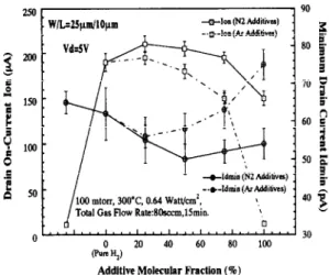
W/lASpm/lOpm I - 70 0 1 a . B - 60 ? i 1 -.-ldmin (NZ AddiCn) 100 mton, 3OO’C, 0.64 Watt/cm’.
-.+-ldmia (Ar Additives)
Total Gas Flow Rat&kcm,l5min.
‘_ I ;.
‘,
Additive Molecular Fraction (%)
Fig. 1. The drain on-current and the minimum drain current of the poly-Si TFTs treated with various additive molecular fractions. The device channel length and channel width are 10 and 25 pm respectively, and the drain voltage is 5 V.
of the plasma treatments were conducted under the substrate heating at 300°C for 15 min. The molecular fractions of the mixed gases in the plasma reactor were varied by feeding the nitrogen and hydrogen with different flow speeds but a constant total gas flow rate of 80 seem. The chamber pressure was kept at 100 mtorr with the power density of 0.64 W/cm*. Figure 1 shows the drain on-currents at Vg = 20V and the minimum drain currents of the poly-Si TFTs treated with various nitrogen molecular fractions. As can be seen, the drain on-currents for the passivated samples are significantly higher than the unpassivated ones and depend on the nitrogen molecular fraction. As compared with the pure H, passivated specimens, the drain on-current for the H,/N, passivated samples initially increases with the addition of the nitrogen plasma. When the nitrogen molecular frac- tion exceeds 25%, the drain on-current gradually decreases with increasing nitrogen molecular fraction. On the other hand, the minimum drain currents also exhibit a monotonic decrease with the minimum value occuring at the nitrogen addition of 50%.
Two possible mechanisms can be used to explain the predominant passivation effects for the nitrogen additives in hydrogen gas over the pure H, hydrogen- ation. The first mechanism is the avalanche process in the plasma ambient. The plasma formation is induced by the radical collision in the reaction chamber. For the larger atomic weight and volume of nitrogen atoms than hydrogen ones, the nitrogen additives will therefore urge the hydrogen to form the radicals by increasing the collision probability. This physical effect would result in the higher concentration of the hydrogen radicals to passivate the poly-Si defects. The second possible cause is the passivation effects of the nitrogen radicals themselves. Since the passiva- tion effects were also observed, even for the pure N2 plasma treatment, we deduce that the passivation effect of nitrogen plasma is attributed to the triple-
Plasma process characterization for TFTs 1235
20
1,
d1. 1, 1, 1, 11
I,1
0 0.16 0.32 0.48 0.64 0.8 0 Radio-Frequency Power Density (Watt/d?)
0 40 80 120 160 0
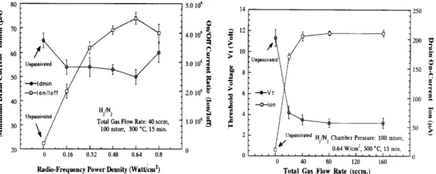
Total Gas Flow Rate (seem.) Fig. 2. The curves of the minimum drain current and the
on/off current ratio vs the RF power density for the poly-Si
Fig. 4. The curve of the threshold voltage and the drain on-current of the poly-Si TFTs against the total gas flow
TFTs. rates for the poly-Si TFTs.
bond passivation of nitrogen radicals to form Si-N
bonds with the poly-Si defects, like those of the Si-H
ones. However, the nitrogen atoms would increase
the sheet resistance due to the increasing electron-
scattering probability, which will result in the de-
crease of the drain current. Hence. the experimental
results show that the addition of 2550% nitrogen
can obtain the optimum drivability improvement.
To further realize the mechanism of HZ/N2 plasma
hydrogenation. the HJAr plasma passivation were
also performed for comparison. It is found in Fig. I,
the passivation effects were also achieved with the
addition of Ar molecular to the hydrogen plasma.
However, no performance improvement was ob-
served for the pure Ar passivated specimens, which is
very different from the pure N, passivated ones. The
disappearance of the passivation effect for pure Ar
plasma treatment is realized for the electron configur-
ation of inert gas structure. The better device per-
formance of the 25% Ar addition is attributed to the
collision between argon and hydrogen radicals. which
14 250
HJN Totll GasFlaw Rate:40sccm, .?
100 mlorr, 0.64 W/cm'. 15 min.
.I.'
27 150 250 300 350 Substrate Temperature (“C)
Fig. 3. The threshold voltage and the drain on-current of the poly-Si TFTs as functions of the substrate heating tempera-
tures.
could enhance the hydrogen to form more of the
radicals than the pure Hz plasma hydrogenation. As
for the increase of minimum drain current for the
higher additives fractions, it is ascribed to the induced plasma damages.
Hence, the addition of nitrogen in the plasma
hydrogenation will improve the passivation effects.
Since the data mentioned above show that the 50%
molecular fraction of the nitrogen in the hydrogen
can obtain the largest on/off current ratio, the Hz/N2 plasma with such a condition are chosen to deal with the following experiments.
2. Eflects of‘ the radioyfreyuency (RF) power den -
sity. To further understand the roles of the RF power
density in the HJN, plasma passivation, TFTs
treated with different RT power densities were also
investigated. The parameters of the substrate heating.
chamber pressure, total gas flow rate and treating
time were fixed at 300 C, 100 mtorr. 40 seem and
15 min with the power densities varied from 0.16 to 0.8 W/cm’ by 0.16 W/cm’ per step. The curves of the
minimum drain current and the on/off current ratio
vs the RF power density are shown in Fig. 2. As can
be seen the devices performance are improved with
increasing the RF power densities. It can be explained
by the avalanche multiplication process of the
plasma. When the RF power density increases to be
above 0.8 W/cm’, the minimum drain current in-
creases due to the large amount of the damages
induced by the high-power plasma. Hence. an appro-
priate RF power density is necessary for the optimum passivation condition.
3. I@ences of’ the substrate heating. gas, flow rate and Amber prrssure. Figure 3 shows the threshold
voltage and drain on-current passivated with H,jNI
plasma as function of the substrate temperature. It is
found that only slight reduction of the threshold
voltage and minor improvement of the drain drivabil-
ity for the plasma treatment with the substrate heat-
1236 M.-J. Tsai et al.
Fig.
3.0 lo6
2.0 lo6 1
1.0 lo6 : Uopmivakd 0.64 W/cm*, 300 ‘C, 15 min.
: J 0 .““I”“““““,‘,
50100 250 500 750 loo0
Chamber Pressare (mtorr)
5. The on/off current ratio of the poly-Si TFTs passi- vated with different chamber pressures.
of the device characteristics occurs as the substrate temperature increased from 150 to 250°C and be- comes saturated as the substrate temperature in- creases above 300°C. The sufficient substrate heating can enhance the radical diffusion along the grain boundaries and the poly-Si/oxide interface as well as the promotion of the plasma generation near the wafer surface by increasing the surface energy.
Figure 4 shows the curve of the threshold voltage and the drain on-current of the passivated poly-Si TFTs against the total gas flow rates. It is found that the device performances rapidly increase with the total gas flow rate and then saturated as the total gas flow rate excess 40 seem. Since the molecular hydro- gen and nitrogen can be easily dissociated under the RF power density of 0.64 W/cm’, the plasma radicals for the passivation will increase with the total gas supply under such a power density. As for the saturation of the characteristics improvement at the flow rate increases above 40 seem, it is because of the shorter residence time for the injected gas with the higher gas flow rate.
The on/off current ratios for the devices passivated with the total pressures varying from 50 mtorr to 1 torr are shown in Fig. 5. Significant improvement of the device performance occurs for the increase of the chamber pressures. Larger chamber pressures mean higher gas contents, leading to higher densities of the active radicals for the high enough RF power density. However, the higher chamber pressures result in the shorter mean free path of the radicals due to the increasing collision probability, leading to the de- crease of the plasma acceleration path and being unfavorable to the HJNz passivation effects. (B) The H,IN,passivation on the TFTs with difSerent film structures
In this section, poly-Si TFTs with different grain structures were passivated with the H,/N, plasma at the RF power density of 0.64 W/cm’, the substrate heating of 3OO”C, the chamber pressure of 500 mtorr,
Fig. 6. The microstructure of the (a) HA film and (b) LL film.
and the total gas flow rate of HZ/N2 (1: 1) mixed gas of 80 seem for 30 min.
According to the TEM inspections, an equiaxed grain structure with the average grain size of about 40 nm for the AP film and a dendritic grain structure with the average grain structure of about 200 nm for the LA specimen were observed. They are consistent
-O-LA -+LL
-10 -5 0 5 10 1s 20
Gate Voltage Vg (Volt)
Fig. 7. The transfer curves of the poly-Si TFTs with various active layers before the HI/N2 plasma passivation.
Plasma process characterization for TFTs 1237
with the previous reports[l2,13]. The TEM picture of
the HA sample displays the coexistence of the
equiaxed and dendritic grain structures with the
average grain size of about 100 nm, as shown in Fig. 6(a). For the LL specimen, the cellular grain structure with the grains as large as several pm in size are attained, as shown in Fig. 6(b).
The transfer characteristics of the poly-Si TFTs
with the different grain structures before and after the
HJN, plasma treatment are shown in Figs 7 and 8.
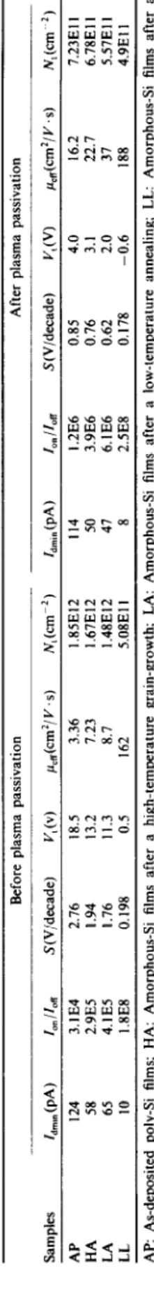
The extracted electrical parameters including the
minimum drain current, the on/off current ratio and
the subthreshold slope, are listed in Table 1. In
addition, the threshold voltage and the field effective mobility measured with the drain voltage at 0.1 V as well as the trap state density calculated in accordance
with the grain-boundaries trap model[l4] are also
listed in the table.
For the TFTs before the passivation, the LL
specimen possessed the best electrical characteristics.
it is attributed to the largest grain size. For the
devices after the passivation, all of the specimens
except the LL film reveal significant improvement in
the electrical characteristics. The reason for the minor passivation effect on the LL specimens is ascribed to the large and perfect grain structure with inherent low trap state density. Since the trap state density for the
unpassivated LL samples does not exhibit obvious
variation after the HJN, passivations, the negative
shift of the threshold voltage for the passivated
specimens can be attributed to the accumulated posi-
tive charges from the H,/N2 plasma in the oxide or
at the poly-%/oxide interface. Except the LL films,
the LA samples still possess the better device per-
formances than the poly-Si TFTs with the AP and the
HA films not only before but also after the HZ/N,
passivation. Furthermore, the performance-order of
the TFTs with various poly-Si grain structures after
the H2/N, passivation is the same as that before
passivation. Larger poly-Si grains and microstructure
with lower trap-state densities are therefore
-I5 -10 -5 0 5 10 15 20 25 Gale Vollage vg (Volt)
Fig. 8. The transfer curves of the poly-Si TFTs with the different active layers after the H,/N, passivation.
1238 M.-J. Tsai et al. considered as the major factors to determine this
order for these TFTs before and after the H,/N, plasma passivation.
4. SUMMARY AND CONCLUSIONS
The nitrogen additives in the traditional hydrogen plasma passivation have been studied. The addition of nitrogen atoms into the hydrogen gas can promote the radical generation by physical collision as well as the passivation effect of nitrogen radicals by forming Si-N bonds. Experimental results show that 25-50% molecular fractions of the nitrogen additives in hydrogen plasma can achieve the better device performances than the pure-hydrogen plasma treat- ment. The optimum plasma passivation effects was also achieved by properly chosen RF power density, gas flow rate, and chamber pressure. In addition, the Hz/N, plasma will also exert the similar passivation
effects on the poly-Si film structures. Consequently, the better the electrical properties of the poly-Si before the H,/N, plasma treatments, the better the device characteristics after the passivations.
Acknowledgements-The research was supported in part by the Republic of China National Science Council under the Contract No. NSC-83-0404-EOO9-050. The research was supported in part by the Republic of China National Science Council (RGC NSC) under the Contract No. NSC-83-0404- EOO9-050. The technical support from the Semiconductor
Research Center and the National Nano Device Laboratory of RGC NSC is also acknowledged. 1. 2. 3. 4. 5. 6. 7. 8. 9. 10. 11. 12. 13. 14. REFERENCES
W. G. Hawkins, IEEE Trans. Electron Devices ED-33, 477 (1986).
M. Yuki, K. Masumo and M. Kunigita, IEEE Trans.
Electron Devices ED-36, 1934 (1989).
M. Rodder and S. Aur, IEEE Trans. Electron Device L.ett. EDL12, 233 (1991).
S. D. S. Malhi, IEEE Trans. Electron Devices ED-32, 258 (1985).
I. W. Wu. T. Y. Huane. W. B. Jackson. A. G. Lewis and A. Chiang, IEEE Trans. Electron Device L.&t. EDL-12, 181 (1991).
M. K. Hatalis and D. W. Greve, J. appl. Phys. 63,226O (1988).
W. G. Hawkins, J. E. Black and C. H. Griffiths, Appl.
Phys. Lett. 40, 319 (1982).
U. Mitra, B. Ross and B. Khan, J. Electrochem. Sot. 138, 3420 (1991).
M. Rodder and D. A. Antoniadis, IEEE Electron Device Lett EDM, 570 (1985).
H. J. Singh, K. C. Saraswat, J. D. Shott, J. P. Mcvittie and J. D. Meindl, IEEE Electron Device Lett. EDL-6, 139 (1985).
S. Seki, 0. Kogure and B. Tsujiyama, IEEE Trans.
Electron Devices ED-35, 669 (1988).
T. I. Kamins, M. M. Mandurah and K. C. Saraswat, J.
Electrochem. Sot. 125, 927 (1978).
A. Nakamura, F. Emoto, E. Fujii, A. Yamamoto, Y. Uemoto, K. Senda and G. Kano, J. appl. Phys. 66,424s (1989).
J. Levinson, F. R. Shepherd, P. J. Scanlon, W. D. Westwood, G. Este and M. Rider, J. appl. Phys. 53,