CMOS Dual-Wideband Low-Noise Amplifier in
3.1
GHz-4.9GHz and 6.0GHz-
10.3GHz for
Ultra-Wideband Wireless
Receiver
Zhe-Yang
Huang',
Che-ChengHuang2, Chun-Chieh Chen3 and Chung-ChihHung'
Dept. of Communication Engineering,National Chiao Tung University, Hsin-Chu, Taiwan2InstrumentTechnology ResearchCenter, NARL,Hsin-Chu, Taiwan
3Dept.of Electronic Engineering, ChungYuanChristianUniversity, Chung-Li, Taiwan
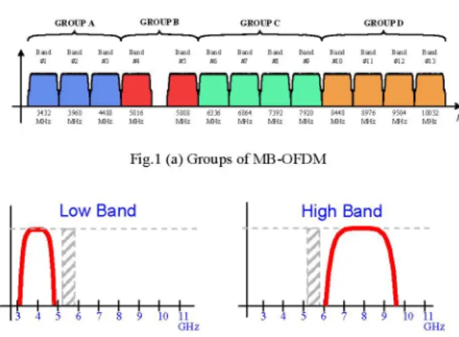
Abstract-Inthis paper aCMOS dual-wideband low- GROUPA GROUPB GROUPC GROUPD
noise amplifier (LNA) is designed for ultra-wideband , Bad Bad Bad
B-d
Bad Bad Bad Bad Band Band Band Band Band (UWB) wireless receiver radio system. The design consists #1 #2 #3 #4 #5 #6 #7 #8 #9 #10 #11 #12 #13of a wideband input impedance matching network, two
stage cascode amplifiers with shunt-peaked load, a notch
34236-4851
8863 8479 9084 9690 03 filter and an output buffer for measurement purpose. It is MHz MHz MHz MHz MHz MHz MHz MHz MHz MHz MHz MHz MHz simulated in TSMC 0.18um standard RF CMOS process.The LNA gives 13.66dB maximum power gain between Fig.1 (a)Groups of MB-OFDM 3.OGHz-4.9GHz and 10.34dB maximum power gain
between 6.OGHz-10.3GHz while consuming 24.07mW Low Band High Band
through a 1.8V supply. Over the 3.IGHz-4.9GHz l== ..========= frequency band and the6.0GHz-10.3GHz, a minimum noise
figure is 2.6dB and 3.8dB. Input return loss lower than
-8.31dB in all bandwidth have been achieved.
35 6 0 1 lo I
Index Term - RFIC, Ultra-Wideband, UWB, Notch 67891011 z4 6 0
Filter,LNA and Low-Noise Amplifier. Fig.I(b)LowBand andHighBandofDS-UWB
I. INTRODUCTION Thispaper is focused onthe designandimplementation
of dual-wideband systems which avoids theU-NII band
Since the approval of the ultra-wideband (UWB) and coexists with MB-OFDM and DS-UWB radio
radio technology for lowpowerwireless communication
systems.
The dual-wideband low-noiseamplifier
forapplication
app cat1ninFebruary,
1nFeruar, Z2002,[1]
UWBUWo systemssytemslashas ultra-widebandStandard RF CMOS Process.receiver isimplemented
in a0.1
8um become an increasingly popular technology which iscapable of transmitting data over a wide spectrum of
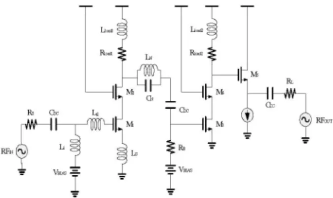
frequency with very low power and high data rate. II. DESIGN OFULTRA-WIDEBANDLNA Although theIEEE UWBstandard (IEEE 802.15.3a [2])
has not been completely defined, two major proposed The
proposed
low-noiseamplifier
is showninFig.2
solutions, MB-OFDM andDS-UWB, are all allowedto which consists of widebandinput impedance matching
transmit in a band between 3.IGHz-10.5GHz and networks, two stages cascode amplifier with shunt-3.1GGHz-9.6GHz. The 1st generation device in peaked
load,
a notch filter and an output buffer. The commercialapplications
for ultra-wideband radioconstituent
of widebandmatchingnetworksareinductors systemswhich shows inFig.I(a)andFig.I(b). The band Li, L2 and Ls and transistor Ml. First stageg cascoded definition ofMB-OFDMis illustrated inFig.1 (a) whichamplifier
are transistors Mi and M2 withshunt-peaked
extended from 3168MHz to 10296MHz and the band load consists of inductors
Lloadl,
Roadi,
and the second definition ofDS-UWB are from 3100OMHz to 4900MHz stage cascodedamplifier
aretransistors
M3 andM4with
and 6000MHz to 9700MHz. The bandwidth of MB-shunt-peaked
loadconsists
ofinductor
Lload2 and Rload2. OFDM iscontaining Group-A, Group-C
andGroup-D.
The notch filter is between firststage
and secondstage
The Group-B is not considered incurrent UWB systemamplifier.
Acommon-drainamplifier
is agood
choice of which causedby
the U-NII band and WLAN(IEEE
wideband outputimpedance
matching for measurement 802.1la). Thebandwidth of DS-UWB is with Low-Band purposeandHigh-Bandwhich is inFig.1(b).
418
L.di Ljd2 Lloadl X
R.cdi Rloa2 RI..dl
L &<LL G I M2 Rs Ccc Lg9 RFu
-CcL
C~~~~~~~~vL~
~
~
~ ~ ~ ~ ~ ~~~~~L
VBIAI(ES VASM(RFX,
YL5
v"T
-
TVu
Fig.2ProposedLow-NoiseAmplifierfor UWB System Fig.3CascodeAmplifierwith Shunt-Peaked Load
A. Wideband
Input Impedance Matching
Agi
S2
RLI
+
SLLL
(5)LI
sCLL
+sCLL
+1
Wideband input impedance matching is a tough design Li Li Li Li challenge in ultra-wideband system. Some excellent
wideband input impedance matching solutions are Amplifier with shunt-peaking load, the power gain and proposed in
[3].
Equation (1) is the parallel LC-tank in the bandwidth is determined by the resistance of load, RF signals input path which resonates a centred where the resistance is small then the quality factor (Q) frequency fri shows in equation (2) where Li is the is high and on the contrary the quality factor is low. The inductor at bias and CLI is the parasitic capacitors. higher quality factor makes higher power gain but Inductive source degeneration also resonate a centred narrower bandwidth, the lower quality factor makes frequency fr2 which are equations (3) and (4) where Lg is lower power gain but wider bandwidth which shows in the gateinductor, Ls is the source inductor and the Cgsi is Fig. 4.the gate-sourceparasitic capacitor in transistor Mi. The
wideband input impedance matching is composed of H 0
thesetwocentredfrequencies fri and fr2.
Z1
=
sL1
1|
SCLi
-.
=IS21
(1)
Low1+2ICLiLo0
frI
(2)
2zf
LiCLI
Fig. 4 Power Gainand BandwidthV.SQuality Factor1 g
~
1SLg
+ + C LSLg
+ C +CTLS
(3) C.WidebandAmplifier
Designsgsl
g1cgsl
gcsi
i gsi g Wide bandwidthamplifier is shown in Fig. 5 which
1 _ (4) consists oftwo stages of shunt-peaked amplifiers. The
2f L g power gain is not
good
enough
when the bandwidth iswidetoreach whole bandwidth of the single stage shunt-peakedamplifier. Therefore, two stages ofshunt-peaked B. Shunt-PeakedAmplifier amplifiers could achieve higher power gain and wider
bandwidth. The cascoded
shunt-peaked amplifier
is easy toreach wide bandwidth which shown in Fig. 3. Cascoded
L1.dl
L1.d2 amplifier eliminates the Miller effect on input transistorto achieve high-frequency performance. Voltage gain
RI1.dl
Ri1ad2
ALi is a band-pass filter type which is expressed in
equation (5). M2 M4 Lg CDC -1 L MI M3 RB -Ls _VBIAS
Fig. 5 Wide Bandwidth Amplifier
The first stage shunt-peaked amplifier is providing the (S11/S22) are lower than -8.31dB/-11.47dB between power gain of lower frequency, and the second stage 3.1GHz to 4.9GHz, respectively. The power gain shunt-peaked amplifier is providing the power gain of whose peak value is 15.65dB at 4.8GHz which covers the higher frequency, which are the blue lines in Fig. 6. the Group-A for MB-OFDM and Low-Band for DS-And final power gain of the low-noise amplifier is the UWB, and is shown in Figure 10. In Fig. 11, it can be red line in Fig. 6 which is the result of two stage shun- seen that the noise figure is below 3.3dB between peaked amplifiersingain compensated. 3.1GHz to 4.9GHz and the minimum noise figure is 3.30dB at4.2GHz through 1.8V supply voltage. InFig. 12,the input-referred1dBcompressionpoint (IPldB) is -27dBm at 4.0GHz. In Figure 9 that can be seenthat the
input/output
return loss(S 1/S22)
are lower than-9.50dB/-9.95dB between 6.0GHz to 10.3GHz, _______________________________________ respectively. The power gain whose peak value is 11.55dB at 9.0GHz which covers the Group-C and Fig.6GainCompensated of Two Stages Amplifiers Group-D for MB-OFDM and High-Band for DS-UWB, and the powergain areshowninFigure 10. InFig. 11, it D. Notch Filter Design canbe seenthat the noisefigureis below6.1dBbetween 6.0GHz to 10.3GHz and the minimum noise figure is There are some signals which are larger than UWB 3.80dB at 6.8GHz through 1.8V supply voltage. InFig. signals in U-NII band, such as WLAN (IEEE 802.11a), 12, theinput-referred1dBcompression point (IPldB)is -and dodging these large interferences is very 22dBm at 8.5GHz. The IIP3 performance is not indispensable. A notch filter is proposed in dual- presented in thispaperbecause the UWB system uses a wideband low-noise amplifier which is located among very wide bandwidth and there is no specified first stage amplifier and second stage amplifier shown in fundamental frequency. Therefore, it does not have Fig. 7. This is a LC-tank series in RF signal path, the meaningto discuss carrier interference with its harmonic impedance is declared in equation (6) and the centred frequency. Thepowerconsumptionis 24.07mWthrough frequency fN is expressed in equation (7). The centred 1.8V supply voltagewhichneglectsthepower ofoutput frequency fN is design at 5.5GHz to reject the buffer.
interference from 5.1GHz to 5.9GHz, and the final power 2
gain is shown in Fig.8. The green line is the final power
od
B---
---1---)I----)----
dBS(2.2)
whichrejects 5.1GHz to 5.9GHz. -2
X----
dB(S(22))-C:N ,,qj ff
Co
-18--Fig. 7 Notch Filter among First and Second Stage Amplifier F< -2o- ^@:
_12 _---r--- n---m--s--- ---- -r
----ZN = PSLN 11
(6)
SLN-2-
4I-1
SCN 1+S2LNCN
O020
2 4.00 6.00 8.00 10.00 12.001 Frequency
2 ~~~~~~~~~~~~~(7) Fig.9 Input Return Loss (SlI) & Output Return Loss (S22)
JN2f LNC 20 dB 2,
15 -
-Fig. 8PowerGain Caused by Notch Filter -.I' .
---.---<.---.---24---III. SIMULATIONRESULTS
-0-0.0 2.OG 4.0G 6OG 8.OG 8OG 12.OG 140OG 162.OG 18OG
The simulation results of the proposed dual- Frequency
wideband UWB LNA using Agilent ADS 2005A Fig. 10 Power Gain (S21) simulator are given in Figure 9 to Figure 12. In Figure 9
that can be seen that the input/output return loss
2 2-I-u-NFmin IV. CONCLUSIONS
20 ---- .f(--- 2)
--- ---wideband system for 3.1-4.9GHz and6.GHz-10.3GHz.
S 14- t
.---,---.---The
simulation results show that the proposed LNA---
bandwidth
10.34dB power gain for 6.0-10.3GHz. 2.4GHz 3dB(2.9 -
5.14GHz)
and4.5GHz
3dB bandwidthZ --- (6.0 --10.5 GH) while consuming 24.07mW through
0.0 2.00 4.00 6OG 8.00 10.00 12.00 ACKNOWLEDGMENT Frequency
Theauthors
would like
tothank the chip implementatLon
line-- ---
gives1366dBcenter
(CIC)for technical support._-F-FOutput
- REFERENCES
20- --- . --- [-1-] FCC,-FinalRule of the FederalCommunicationsCommission, 47
30:
CFR Part 15,Sec. 503", Federal Register, vol. 67,no. 95,May 2002.F y[3] Andrea Bevilacqua, and Ali M. Niknejad," An Ultrawideband
Fig.I I CMOS Low-Noise Amplifier for 3.1-10.6-GHz Wireless
lineReceivers",IEEEJOURNALOF SOLID-STATE CIRCUITS, Vol.39,
60- No.12,pp.2259-2268,Dec 2004.
060 - 50 - 40 - 30 - 20 - 10 0
InputPower(dEm) [4] Chang-Wan Kim, Min-Suk Kang, Phan TuanAnlh,Hoon-Tae Kim, Fig. 12 Input-Referred1dBCompressionFPoint and Sang-Gug Lee, 'An Ultra-Wideband CMOS Low Noise Amplifier for 3-5-GHz UWB System", IEEE JOURNTAL OF SOLID-STATE CIRCUITS, Vol. 40, No. 2,pp.544-547, Feb. 2005. 3.1-4.9GHz 6.0-10.3GHz [5] Chang, C.-P.;Chuang, H.-R., 0.18 um 3-6 GHz CMOS broadband
Sl1(dB) <-8.31 <-9.50 LNA for UWB radio", Electronics Letters, Volume 41, Issue S22 (dB) < -11.47 < -9.95 12, June 2005 Page(s):33 - 34.
S21 (dB) 12.15-15.65 |8.95-11.55 [6] Yang-ChaunChen; Chien-Nan Kuo, "A 6-10-GHz ultra-wideband S21 Max. (dB) 15.65 |C11.55 tunable LNA", Circuits and Systems, 2005. ISCAS 2005. IEEE I ~~~~~~InternationalSymposium on, 23-26 May 2005 Page(s):5099 - 5102 WorkingBandwidth (GHz) 3.1 -4.9 6.0-10.3 Vol.5.
3dBBandwidth (GHz) 2.95.1 6.010.52
NE (dB) 2.6 -3.3 | 3.8 6.1 [7] Chih-F aLiao;n Shen-duan Liu, "A broadband noise-canceling ---CMOS LNA for 3. 1-10.6-GHz UWB receiver, Custom Integrated
IPldB (dBm) -27 -22 CircuitsConference, 2005. Proceedings of theIEEE 2005, 18-21
IIP3(dBm)[lOMHNoz] -18 -12 Sept. 2005Page(s):161-164. Power Consumption (mW) | 24.07
Table. 1PerformanceComparisons
Paper CircuitTopology Technology 51Sl(dB) |S22(dB) |S21(dB) BW(GHZ) Gmax(dB) tNF(dB) |NFmin(dB) |Pdiss(mW)
[4] resistive feedback 0.18umSCMOS <-9 <V-10 6.8-9.8 2.0-4.6 9.8 2.3-5.2 2.3 12.6 [5] 3-stages comm.-source 0.18umCMOS <-12.2
<3-10.1
13.5-15.8 3.0-6.0 15.76 4.7-6.7 4.7 59.4 [6] TunableLC-ta<k0. 8um CMOS <-9 < -12 10.0-11.6 6.0-10.0 11.6 4.2-5.3 4.2 11.6 [7] 3-stages shunt-peaked 0.18umCMOS <7 <-12 6.7-9.7 1.2-11.9 9.7 4.5-5.1 4.5 20.0 3-4.9GHz 2-stages shunt-peaked <-8.3 <-11.5 12.2-15.7 2.9-5.1 13.66 2.6-3.3 2.6(Thiswork) with 0.18umCMOS <-9.5 <-9.9 9.0-11.6 6.0-10.5 10.34 3.8-6.1 24.1
6-10.3G notch filter
Table.2 Comparisonof the Proposed UWB LNA with Other ReportedWidebandLNA