www.pss-rapid.com
pss
Part of Focus Issue on Functional Oxides Eds.: T. Frauenheim, J. M. Knaup, P. Broqvist, S. Ramanathan
Controllable electrical conduction
at complex oxide interfaces
Vu Thanh Tra1
, Jan-Chi Yang2
, Ying-Hui Hsieh2
, Jiunn-Yuan Lin1
, Yi-Chun Chen3
, and Ying-Hao Chu*, 2, 4 1 Institute of Physics, National Chiao Tung University, Hsinchu 30010, Taiwan
2 Department of Materials Science and Engineering, National Chiao Tung University, Hsinchu 30010, Taiwan 3 Department of Physics, National Cheng Kung University, Tainan 70101, Taiwan
4 Institute of Physics, Academia Sinica, Taipei 105, Taiwan Received 3 April 2014, revised 19 May 2014, accepted 19 May 2014 Published online 30 May 2014
Keywords complex oxide interfaces, heterointerfaces, homointerfaces, tubular interfaces, electron conduction, LaAlO3/SrTiO3, BiFeO3/CoFe2O4
* Corresponding author: e-mail [email protected]
© 2014 WILEY-VCH Verlag GmbH & Co. KGaA, Weinheim
1 Introduction to complex oxide interfaces
Complex oxide interfaces have emerged as one of the most exciting fields in condensed-matter physics, owing to their unique physical properties and exhibiting a wide range of phenomena such as magnetism with high Curie tempera-ture, high-temperature superconductivity, ionic conduction or metal–insulator transitions, and multiferroicity. Nobel laureate, Herbert Kroemer, coined the phrase “the interface is the device” [1], which triggered a frantic search to find new possibilities for next-generation electronic devices based on oxide interfaces, including batteries, fuel cells, in-formation storage and so on [2–4]. In addition, oxide inter-faces between strongly correlated electron systems not only provide a powerful route to manipulate the charge, spin, orbital, and lattice degrees of freedom but also offer a unique opportunity to control and enhance the effects by controlling the interactions between functional layers [2, 5, 6]. Complex oxide interfaces serve as a key role holding
the promise for new multifunctional properties that cannot be realized by the individual single-phase bulk materials [2]. In this review, the main focus will be the three impor-tant types of complex oxide interfaces, as illustrated in Fig. 1.
The artificially constructed heterointerface (Fig. 1a), which is formed by the topological boundaries in het-erostructures composing of two or more layers of different materials, is one of the most well explored oxide interfaces. Recently, heterointerfaces have created a hot paradigm in the complex oxide community due to the fact that techno-logical successes came together with the discovery of new quantum phenomena in heterointerfaces. Unlike the hetero-interfaces, which are composed of different materials, ho-mointerfaces were discovered as a consequence of the minimization of electrostatic and elastic energies in ferroic systems (Fig. 1b). The developments and understanding of the ferroic homointerfaces have driven both scientific in-Oxide interfaces have sparked considerable interest due to
their fascinating physical properties and promising possibili-ties for next-generation nanoelectronics. Three intriguing ox-ide interfaces, hetero-, homo-, and tubular interfaces, will be discussed in detail in this review. First, the development and fundamental properties of classical heterointerfaces will be elaborated. Using LaAlO3/SrTiO3 as a case study, we present the most generic approach to control the two-dimensional electron conduction at the heterointerface. Secondly, several key issues based on interesting observations on ferroic
homointerfaces will be addressed. Multiple controls of fasci-nating functionalities based on multiferroic BiFeO3 domain walls will be presented as a model system. Finally, as the most challenging task, we review a new type of complex ox-ide interfaces, the tubular interface. Further insights of re-cently emerged tubular interfaces in BiFeO3/CoFe2O4system will be explored, which serve as one of the focal roles in de-veloping new functional interfaces and potentially new type of nanostructures.
terests and promising functionalities. More recently, the emergence of multiferroics, materials with coexistence of different parameters, has triggered a new possibility for creating multifunctional homointerfaces, makes homointer-faces appealing for room-temperature applications and no-vel multifunctionalities. However, the complexity of ho-mointerfaces has hindered the exploration of real applicati-ons. As a result, developing a modeling system to pave the pioneering route is required and will be presented in the following section of heterointerfaces. Last but not least, a special focus will be placed on tubular interfaces found in self-assembled nanostructures, which create a huge play-ground to discover new emergent phenomena (Fig. 1c). Among the various self-assembled systems, the vertical he-teroepitaxial nanocomposites have offered promising ca-pabilities to create intriguing functionalities through the in-terplay between different degrees of freedom and external stimuli of the selected materials [7, 8]. However, the studies on tubular interfaces are still in the preliminary stage, where further insights and development should be gained to expand the infinite possibilities of such interest-ing interfaces. We will discuss the findinterest-ing, development and advanced control of the tubular interfaces in the final section.
Vu Thanh Tra received his Ph.D. in Phys-ics (condensed master physPhys-ics) in 2013 from the Institute of Physics, National Chiao Tung University, Taiwan. After his graduation, he has worked at National Chiao Tung University (Taiwan) as a post-doctoral fellow, sponsored by Natio-nal Science Council, Taiwan, since 2013. His main research interests are complex oxide interfaces and nanostructures (fabrication and characterizations) for next generation electronic devices. He is also interested in low temperature physics and topological defects in strongly corre-lated systems. Now, he continues the activity of Smart Group of Prof. Chu in the Department of Material Sciences and En-gineering, National Chiao Tung University in Hsinchu, Tai-wan.
Ying-Hao Chu obtained his Ph.D. in 2004 from the Department of Material Sciences and Engineering, National Tsing Hua University, Taiwan. After four years working as a post-doctoral fellow at Uni-versity of California, Berkeley, USA, he has been appointed as an assistant profes-sor in the Department of Material Sci-ences and Engineering at National Chiao Tung University, Taiwan in the year 2008. He is now holding an adjunct position both in Institute of Physics, Academic Sinica (2013), and in the Department of Electrophysics, Na-tional Chiao Tung University, Taiwan (2014). His research fo-cus is on complex functional oxides, strongly correlated elec-tron systems and broad experimental characterization tech-niques to understand and manipulate complex functional oxide heterostructures, nanostructures, and interfaces.
In light of the rapid development of state-of-the-art deposition, all tools such as the oxide molecular beam epi-taxy (MBE), pulsed laser deposition (PLD), sputtering or atomic layer deposition, are very useful to construct the complex oxide interfaces. In this study, all epitaxial inter-faces were grown by PLD with assisted reflection high-energy electron diffraction (RHEED), it is now practical to routinely fabricate atomically perfect and high-quality complex oxide interfaces as shown in Fig. 1. The details of the sample-preparation characterizations for typically each kind of interface can be found in [7–10].
2 Heterointerfaces The formation of
heterointer-faces occurs when two different materials are intimately connected. In particular for the heterointerfaces in complex oxides, they provide more possibilities to manipulate the lattice, orbital, charge, and spin degrees of freedom, resul-ting in a number of exciresul-ting discoveries and serve as an unmatched role for creating diverse physical phenomena. For example, the discovery of novel phenomena such as the integer and fractional quantum Hall effects (QHE) at the heterointerfaces of ZnO/(Mg,Zn)O [11] closely
re-semble that of the GaAs/AlxGa1–xAs interface [12].
Another obvious effect is the breaking of the symmetry that may change the electronic, structural and magnetic properties. Moreover, when the complex oxides with diffe-rent chemical potentials meet face to face, charge transfer may take place at the interface. Heterointerfaces in the su-perlattice thin films composed of two antiferromagnetic
Mott insulators, LaMnO3 and SrMnO3, exhibit both
ferromagnetic and metallic tendencies, promote coupling of charge-spin and orbital modulation [13–15]. “Colossal magnetoresistance” observed in the superlattice of
anti-ferromagnetic insulator CaMnO3/paramagnetic metal
CaRuO3 [16] is also attributed to the interface effect. The
high degree of spin polarization of the LaxCa1–xMnO3
(LCMO) conduction band together with the d-wave pairing symmetry of superconducting YBa2Cu3O7–x(YBCO)
dem-onstrates a long-range charge transfer and associated rich phenomena due to the competition between two order pa-rameters at the interfaces [6, 17]. The competition between the interface coupling and the different ground states of bulk BiFeO3 (BFO) and LaxSr1–xMO3 (LSMO) leads to a
spin frustration and thus a novel spin state at the interface or an induced ferromagnetic state in the BFO/LSMO het- erointerface evolves [18]. The ferroelectric control of the interfacial charges in Pb(Zr,Ti)O3/ LaxSr1–xMnO3 [19] is
al-so revealed.
Recently, a 2-dimesional electron gas (2DEG) behavior has been revealed in LaVO3/SrTiO3 [20], LaTiO3/SrTiO3
[21] and LaAlO3-SrTiO3 [5] (LAO/STO) systems and this
had become a most fascinating topic. There are many in-triguing physical phenomena undiscovered in similar sys-tems. The observation of the QHE and 2DEG at the inter-face between two band insulators [2, 5, 22, 23] and a high electron mobility offer a novel platform for Rashba physics, wherein the spin–orbit coupling can be manipulated by the
external field and many other quantum phenomena. In ad-dition, LAO/STO interface possesses ultrahigh mobility, interface superconductivity and colossal magnetoresistance, and multiple tunable features that are important for practi-cal applications. Therefore, in the first section, we will fo-cus on the interface-induced 2DEG behavior, introducing its origin and the control of its conduction at the n-type LAO/STO interface by various methods.
2.1 Recent studies on LAO/STO interface The LAO/STO interface serves as a model heterointerface sys-tem in which a highly mobile quasi-two-dimensional elec-tron gas (2DEG) forms between two band insulators hav-ing mobility values up to 104 cm2 V–1 s–1 at 4.2 K and the
resultant high electron carrier density compare well with other 2DEG based on conventional III–V semiconductor
heterointerfaces [5, 22, 24]. Since then, a number of strik-ing properties of such interfaces have been discovered and explored. To originate the 2DEG in complex oxides, there are several key mechanisms that should be noticed: First, a polar catastrophe/surface [5, 25]; and atomic intermixing [24, 26]. Secondly, the influence of thickness on electronic band structure across the interface or electronic reconstruc-tions at the interfaces. Thirdly, an alternative doping mechanism by oxygen vacancies.
A number of studies show that termination control plays an important role in complex oxide interfaces.
Several prominent examples, such as LaTiO3/SrTiO3
[21], LaVO3/SrTiO3 [20], ZnO/(Mg,Zn)O [11] and LCMO/
YBCO [6] or even BFO/LSMO [18] and also ferroelectric control of the interfacial charges in PZT/LSMO [19], have exhibited that the polarity discontinuity and physical
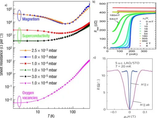
prop-Figure 2 Physical properties at n-type LAO/STO interface: (a) Temperature dependence of the sheet resistance, Rsheet, for n-type LAO/STO conducting interfaces, grown at various partial oxygen pressures (taken from Refs. [29, 32]). Three regimes can be distin-guished: low pressure leads to oxygen vacancies, whereas samples grown in the intermediate regime show superconductivity as dem-onstrated in (b) [33], while the samples grown at high pressures show the coexistence of superconductivity and magnetic ordering in a 5-uc LAO/STO interface sample, as shown in (c), H dependence of R in different field directions taken at T = 20 mK [31].
Figure 1 A huge playground of con-densed-matter physics: various types of complex oxide interfaces: (a) planar het-erointerface, (b) planar homointerface, and (c) tubular heterointerface.
erties are manipulable using different surface terminations. In the LAO/STO system, based on the termination control at STO substrate, it is possible to create n-type or p-type interfaces [5, 27, 28]. Many studies reported that the (LaO)+/(TiO
2)0 interface, where the LAO thin film was
grown directly on TiO2-terminated STO substrate, is
ex-pected to be an n-type conducting interface for a wide range of conditions such as temperature, LAO thickness, and oxygen pressure as shown in Fig. 2a [29]. However, the (AlO2)–/(SrO)0 interface was grown by inserting a
monolayer of SrO from a single-crystal target in between the TiO2-STO substrate and the LAO layer. The latter is
called a p-type insulating interface, although the possibility of Schottky barrier formation exists [5]. This unexpected interface superconductivity, as shown in Fig. 2b, and mag-netism, as depicted in Fig. 2c, is indicative of a further rich variety of emergent properties in oxide interfaces and it should also be considered as a noncentrosymmetric sys-tems [30, 31].
Thiel et al. [23], in 2006, reported that the LAO/STO interface has an interfacial insulator to metal transition de-pending on the LAO thickness. When the thickness of the LAO layer is greater than the critical thickness dc = 3 unit
cells (uc), the n-type LAO/STO interface becomes con-ducting. But when the thickness is below this critical value, the LAO/STO interface remains highly insulating. The re-sult of conduction at an n-type LAO/STO interface, with the Ti valence ideally varying from 3+ to 4+, is due to the charge transfer at the interface. When the LAO thickness is increased further, a progressive charge transfer from the LAO surface to the LAO/STO interface takes place. It is predicted that the holes are formed in the O 2p valence band of the surface layer of LAO, and electrons are accu-mulated at the interface in the Ti d-orbitals (t2g) [24, 27, 29,
34, 35]. In the electronic reconstructions models, one of the still debated issues regarding STO/LAO interfaces is just the nature of the donor states, electrons come from the valence band of the polar layer that is lifted above the Fermi level by the built-in potential due to the polarization. Therefore, some donor states are trapped at the 2DEG [36, 37]. The most basic question here concerns the electronic charge distribution. Chu et al. [34] studied the distribution of electronic reconstruction at the n-type LAO/STO inter-face by hard X-ray photoelectron spectroscopy (HAXPES) under grazing incidence and revealed that the total amount of charge transfer can be estimated to be around 0.24 elec-trons per two-dimensional unit cell, which also implies the existence of the electronic reconstruction in LAO/STO heterointerfaces. In addition, to provide the direct evidence of electronic reconstruction or the evolution of electronic structures across the complex oxide interface in LAO/STO, the cross-sectional scanning tunneling microscopy/spectro-scopy (XSTM/S) study was performed by Huang et al. [38]. Their results showed that the conduction-band edge in STO near the interface is below the Fermi energy (–0.03 V) with an approximate distance (λ) of 0.8 nm (band bending). Therefore, the unusual electronic
proper-ties at the interface of the STO side may originate from the band bending and the accumulation of surface charges in the STO, adjacent to the interface.
Finally, metallic states or charge transport at the LAO/STO interface strongly depend on the growth condi-tions, especially the oxygen partial pressures [5, 22, 39, 40], suggesting that the oxygen vacancies could be an alterna-tive doping mechanism [29, 32]. Brinkman et al. [29] and Rijnders and Blank [32] have shown that the temperature evolution of the sheet resistance on the oxygen pressure is dramatic. There are three main oxygen regimes that can be pointed out, as shown in Fig. 2a.
1. The very low oxygen pressure regime (PO2 ~ 10–6 mbar),
the oxygen vacancies dominate the conduction properties, and a large carrier density is observed.
2. The intermediated regime, (oxygen pressure ranging from 10–4 to 10–2 mbar), low conductivity and mobility are
observed, and the conductivity is believed to be confined to the interface. In this regime, the conductivity at the in-terface also depends on the growth temperature [29, 39].
3. Remarkably, in the high-pressure regime (PO2 ~
10–3 mbar), the interface between two nonmagnetic
materi-als becomes magnetic with very large negative magnetore-sistance, as shown in Fig. 2c [31]. Magnetic effects or coexistence of magnetic order at the interface between nonmagnetic oxides is very clear and strong, and exhibits unusual magnetotransport properties (up to 30% over a magnetic field range of 30 T) [29, 31], which is related to spin physics and Kondo effects [41, 42] and not to the or-bital effects.
Besides looking for the ways to control these exciting properties of systems, we are still working on all the possi-ble applications, especially how one would engineer the conductivity from insulating to metallic sates and transfer it to real devices.
2.2 Control and engineering of the conduction at an n-type LAO/STO interface Controlling or tuning
the conduction at LAO/STO results in potential applica-tions for the semiconductor industry. Motivated by this, the control of the conduction at LAO/STO heterointerface with a critical thickness of LAO being 3 uc was done by several methods.
2.2.1 Electrical top (bottom) gate control One of
the methods is using the electrical top (bottom) gating of LAO/STO heterointerface. First, although a modulation of the 2DEG carrier density and mobility of the LAO/STO in-terface was achieved by using the electric-field effect [23, 43, 44], and used to create Schottky-like devices [45], it is essential to extend the control concepts to gain nonvolatile and reversible abilities for practical applications. When a positive voltage is applied, the interface has a large con-ducting current flow, on the other hand, when the gate bias is negative, the conduction between the gate and interface contact becomes depleted and leads to very low conduction. A second approach of electrical gating is using a bottom
gate where the bias is applied to the bottom of the rela-tively thick (~1 mm) STO substrate. The transport proper-ties of the interface can be modified by applying large voltages to the bottom of the substrate. Thiel et al. were the first ones to demonstrate that the interface can be tuned from insulating to metallic states at room temperature by applying a gate voltage for insulating LAO3 uc/STO sam-ple. Figure 3a shows that one could reversely switch the sheet conductance between ~1×10⁻⁶ Ω–1 and an
unmeasur-able value <2 × 10⁻¹⁰ Ω–1, and later this was confirmed by
several groups. The main reason for exploring the 2DEG at the LAO/STO interface is that it can be applied to fabricate high electron mobility transistor-type field effect devices [23, 46].
2.2.2 Generating 2DEG by using lithography and c-AFM writing nanowires Importantly, the
non-volatile modification of the local conduction at the LAO/STO interface has been demonstrated by scanning probe techniques [47–49]. To create conducting nanostruc-tures, microlithography is a helpful tool for the formation
of electron gases at interfaces in oxide heterointerfaces [50]. For this lithography method to obtain 2DEG a se-quential deposition of epitaxial and amorphous LAO layers demonstrated in Fig. 3b, was carried out. The details of these processes are described as follows: 2 uc of LAO was epitaxially grown and through the use of a lithographic mask and lift off, we produced the structure shown in Fig. 3b. This results in the interface conducting in the re-gions within a total 5 uc of LAO surrounded by insulating regions of 2 uc LAO/STO. Then, lines as small as 200 nm wide were defined by a combination of standard optical UV lithography and electron beam lithography. The con-ducting switching of 2DEG nanowires formed at the LAO/STO heterointerface by also using a writing conduct-ing-AFM tip [28] was grown directly on (001) silicon sub-strate. For the nanoscale writing and erasing method, a conducting 2DEG nanowire is created and produced by scanning the c-AFM tip along the x-axis with a tip poten-tial of positive bias (Vtip = +4 V). During the process, the
c-AFM tip is scanning and writing from one to the other electrode, an abrupt jump in current is observed. When the
Figure 3 (a) Memory behavior of the q2-DEG of an n-type LAO/STO heterointerface. The upper panel shows the sheet resistance measured at 300 K, while the lower panel shows applied backgate voltage, both plotted as a function of time for a sample with d = 3 uc. By applying the gate voltage pulses, we could reversely switch the sheet conductance between ∼1 × 10⁻⁶ Ω–1 and an unmeasurable value <2 × 10⁻¹⁰ Ω–1. The data were measured in four-point configurations [23]; (b) illustration of the patterning technique: (i) on a TiO2-terminated STO substrate 2 uc of LAO are deposited epitaxially; (ii) on a resist lift-off structure, 10 nm of amorphous LaAlO3 are grown, and then 3 uc of LAO are deposited. At the LAO/STO interface the q2-DEG is formed at the areas defined. Finally, a sketch of a cross-sectional view of the sample (iii) [50]. (c) Processes of writing and erasing a nanowire at the LAO/TiO2-STO hetero-interface on Si. (i) Schematic diagram of the ‘writing’ process used to generate conducting nanostructures at the LAO/TiO2-STO het-erointerface. (ii) Electrical conductance between two electrodes during c-AFM writing with Vtip = +4 V. As the c-AFM tip reaches the second electrode, the conductance increases abruptly. The c-AFM tip travels along the x-direction as noted in the figure, with a speed of 400 nm/s relative to the structure. (iii) Schematic diagram of the ‘erasing’ process by cutting the nanowire generated in the writing process. (iv) As the c-AFM tip biased at −4 V scans across the nanowire, the conductance decreases drastically [28]. (d) SketchSET schematic and transport characteristics, c-AFM sketching of a single-electron transistor device [48].
nanowire writing was complete, the tip is repositioned, bi-ased negatively (Vtip = −4 V) and scanned slowly along the
y-direction. When the tip reaches the nanowire, the
con-ductance abruptly reaches zero again (Fig. 3c) which means that the positive tip voltages applied to a c-AFM probe in contact with the top of the LAO surface locally produces a metallic interface, while negative tip voltages restores the interface to its initial insulating state. The switching of the conductance at the interface was found to be repeatable over hundreds of cycles [50]. The charge writing at LAO/STO surface [49], a similar concept to that presented by Wu et al. [51], opens up new opportu-nities to incorporate ultrahigh-density oxide naonoelec-tronic memory devices based on Si platforms. However, one possible explanation for the switching of the conduc-tance at LAO/STO interface between conducting and insu-lating states is believed to be governed by a ‘water cycle’ [52] in which the top LAO surface is locally charged through hydrogen passivation, resulting in high-resolu- tion modulation doping of the LAO/STO interface. Using this technique, it is possible to write nanowires as small as 2 nm wide and islands with a diameter of 1 nm [47, 50]. Cheng et al. [48] reported the creation and electronic characterization of a ferroelectric sketch- based single-electron transistor (SketchSET) as shown in Fig. 3d.
While most of the studies aim to explore new inter-faces by combining different materials, the key to realizing the practical applications is the control through external stimuli as discussed above. More importantly, in the pur-suit of practical applications that we are going to introduce here, it is desirable to have the ability to modulate the in-terface functionalities by ferroelectricity.
2.2.3 Ferroelectric control of the conduction of LAO/STO interface In this particular section,
ferroelec-tric control, we introduce a generic approach by inserting a functional layer to the heterointerface to acquire the non-volatile control of the intriguing properties at oxide inter-faces. As mentioned above, several possible mechanisms have been proposed to explain this interesting behavior and the other results based on the electrostatic effects either attributed to induced ferroelectricity or surface charge [52, 53]. Therefore, in this section, the study in Ref. [9] intro-duces a ferroelectric Pb(Zr0.2Ti0.8)O3 (PZT) layer nearby
the LAO/STO interface. The ferroelectric polarization of PZT layer serves as a control parameter to modulate the 2DEG conducting behaviors.
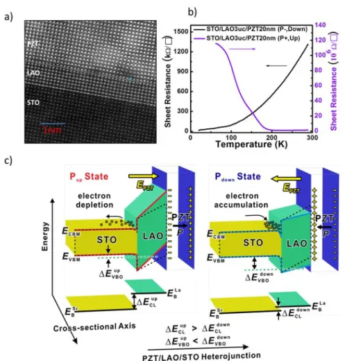
In order to realize this concept, the structural charac-terization needs to be done as the first step. To ensure the quality of the samples, the crystallinity of the heterointer-face was studied using X-ray diffraction techniques. Fig-ure 4a demonstrates that both PZT and LAO are grown epitaxially on the TiO2-STO (001)-oriented substrates and
the scanning transmission electron microscope (TEM) shows the atomically sharp interfaces with the derived cube-on-cube epitaxial relationship, [100]STO(001)STOǁ
[100]LAO(001)LAOǁ [100]PZT(001)PZT. This is in good
agree-ment with the X-ray results [9].
To explore the influence of ferroelectricity on the LAO/STO interface experimentally, electrical transport measurements on the heterointerface were carried out, in which the PZT layer with the spontaneous polarization
PPZT functions as the polarized dielectric slab to modulate
the conduction of LAO/STO heterointerface, with PZT and LAO thickness dependence. The results clearly show the strong impact of the intrinsic polarization (Pup) of PZT on
electron conduction at the interface, which means that un-der the effect of the ferroelectricity of PZT the device be-comes less conducting at the LAO/STO interface. This is anticipated since the ferroelectric field effect provides one more degree of freedom to compensate the charge unbal-ance at the interface [54]. Now, the important question that arises is how the ferroelectricity of PZT can control the conduction at LAO/STO interface. The transport meas-urements have provided a clear insight into the ferroelec-tric effect on the LAO/STO interface. The sheet resistance with natural polarization state (Pup) of as-grown samples is
rather high (the off state). After flipping the polarization by the scanning probe technique to an opposite direction (Pdown), the sheet resistance falls to a low state resistance
(the on state). Another intriguing feature here is the switch-ing of an insulatswitch-ing state to a conductswitch-ing state. The evi-dence of PZT/LAO (3 uc)/STO typically shows insulating behavior. The polarization switching of PZT from the Pup
to the Pdown polarization states can change the transport
be-haviors from insulating to metallic, suggesting the non-volatile control of the metal–insulator transition with ferro-electricity (Fig. 4b). Thus, the transport measurements in-dicate that the ferroelectric field effects can not only modu-late the conduction but also switch the conducting state.
The contribution of the ferroelectric layer of PZT in controlling the conduction at LAO/STO interface can be understood/explained by the model (Fig. 4c) based on the XPS and XSTM/XSTS results and it is very consistent with the transport data presented in Fig. 4b. In the case of a naturally Pup state of capped PZT, the PZT bottom has a
negative polarization charge sheet, the potential built-up in the polar LAO layer increases and the free electrons gets repelled from the LAO/STO interface (electron depletion), where the interface band bending of the STO side de-creases with smaller valence-band offset (VBO) value and makes ΔECL larger. As the polarization switches to Pdown
state, the positive polarization charge sheet at the bottom of the PZT makes the LAO built-up potential decrease and attracts more free electrons at the LAO/STO interface (electron accumulation), where the interface band bending of the LAO side increases with larger VBO value and re-sults in smaller ΔECL. In addition, for the LAO/STO
het-erointerface having a thinner LAO layer (3 uc), the varia-tion of electric potential induced by EPZT can be estimated
to be about 1.0 eV, in which the thickness of the LAO layer thickness is about 1.1 nm (3 uc) and the stray electric field in LAO layer is estimated about 109 V/m. This 1.0 eV
Figure 4 Ferroelectricity modulated conductivity at LAO/STO interface. (a) TEM investigation of the PZT 20 nm on top of LAO 6 uc/STO heterointerface, a high-resolution HAADF image showing an atomically sharp interface of both LAO and PZT films on a TiO2-terminated STO substrate. The dimension of the scale bar is 1 nm; (b) sheet resistance measured as a function of temperature for as-grown PZT 20 nm/LAO 3 uc/STO with natural polarization (Pup) and after switching the polarization to down states (Pdown); (c) schematic band diagrams of a PZT/LAO/STO heterojunction derived from ferroelectric-pattern-assisted XPS and XSTM/S measure-ments. The sheet of negative/positive bound charges at the bottom PZT and its induced E-field (EPZT) across the LAO layer would di-rectly affect the mobile charges depletion/accumulation at the LAO/STO heterointerface, shown for both polarization states (Pup and
Pdown) of the PZT layer. Decrease and increase potential buildups across the LAO layer correspond to different polarization states are indicated. Combining both XPS and STS spectroscopicresults, the changes in valence band offset (ΔEVBO) and core-level energetic separation (ΔECL) between LAO and STO layers are revealed, and a ferroelectricity modulated LAO/STO band structure model is con-structed.
potential variation is three times larger than the built-in po-tential variation of about 0.3 eV from the metal–insulator transition reported in the Refs. [23, 28, 54]. Therefore, ow-ing to a reversible polarization of top ferroelectric layer, the PZT/LAO/STO system is expected to be the one clos-est to having nonvolatile switching on/off characteristics at the LAO/STO interface. The model in Fig. 4c strongly confirmed that as-grown polarization (Pup state) leads to
charge depletion and consequently a low conduction. Switching the polarization direction (Pdown state) leads to a
charge accumulation and enhances the conduction at the interface of LAO/STO. Similar control of the conductivity or capacitance by inducing the polarization was also re-ported by Singh-Bhalla et al. [44].
2.2.4 Control of the conduction at LAO/STO in-terface by adsorbates and nanoparticles It is known
that the surface atoms are significantly affected by adsor-bates. The theoretical calculations were carried out on the dissociation of hydrogen and redox reactions [55–57] at the LAO surface as possible electron sources. Later, the study by Xie et al. [58] experimentally demonstrated that the surface adsorption of common solvents such as ace-tone, ethanol and water can induce a large change in the conductivity and accumulation of electrons at the LAO/STO interface. The schematic shown in Fig. 5a (right) illustrates that the strong polarization in the LAO layer well aligns the polar adsorbates nearest the surface, but displays a decaying trend in alignment as one moves
Figure 5 (a) Sketches of band diagrams and electron-transfer mechanisms: (Left) Idealized surface. Electrons transfer from
EVLAO of the LAO surface to the conduction band of STO ECSTO, near the interface. eVUuncom roughly equals the EgSTO. (Right) Surface with aligned polar adsorbates. Electrons transfer from the surface adsorbates to ECSTO near the interface. The built-in potential across the adsorbates, Vad, effectively reduces VUuncom across the LAO layer. In both (Left and Right), bulk stoichiometry and valences are shown for simplicity. [58] (b) Schematic diagram of the Pd nanoparticle surface modulated by the photoconductivity at LAO/STO het-erointerface with UV-light irradiation [59].
deep into the adsorbate layer. This results in an electro-static potential across the adsorbate layer, Vad, which is
very similar to the built-in potential in the polar LAO. As a consequence, the uncompensated potential, VUcom, across
the LAO effectively decreases and the total sheet electron density at the interface (σInter) increases. Using the surface
adsorption process to control the conductivity at the inter-face, the device switches reproducibly between a high-conductivity state with the surface adsorption process and a low-conductivity state after heating. Moreover, Chan et al. [59] showed that the addition of palladium nanoparti-cles to the LAO/STO heterointerface presents a giant opti-cal switching effect with a very large photoconductivity on/off ratio (750%) under the UV-light radiation, but dif-ferent electrical responses for oxygen, dry air, and argon were observed. The model to explain this enhanced photo-conductivity effect of the palladium nanoparticles is pro-posed in Fig. 5b. Finally, it is more important to emphasize that the nanoparticles or adsorbate-functionalized 2DEG LAO/STO heterointerface may find use in
room-tempe-rature gas sensor applications with high sensitivity. As this structure has high selectivity to oxidization and reduction of gases and a catalytic effect to different gases, a charge coupling between the gas molecules and nanoparticles as well as the 2DEG occurs through either a direct charge ex-change or a ex-change of electron affinity.
These results enrich the physics in the LAO/STO sys-tem and open up a wide range of application potentials in many fields, such as molecular sensing devices and other catalytic applications. So, the control of the conduction at this oxide interface suggests that the concept can be gener-alized for other oxide systems to design functional inter-faces.
2.3 Summary and outlook for heterointerfaces
In short, heterointerfaces serve as an intriguing playground bringing out many fascinating physical properties, such as charge transfer, electrostatic or spin–orbit coupling, epi-taxial strain, magnetotransport, superconductivity, quan-tum Hall effects, and competition between different phases
and other parameters. The metal–insulator transitions ob-served in the correlated electron materials such as LAO/ STO interface provides potential possibilities and novel platforms to design new functionalities. It would be more exciting to tune oxide 2DEGs by adding strong electron correlations and to control the electrical conduction at LAO/STO interfaces by many different methods, as dis-cussed above. In addition, a lot of substantial progress has been made in order to understand the properties of hetero-interfaces in physics and electronics. The progress in oxide thin-film growth, and corresponding innovation have eased the fabrication of high-quality heterointerfaces composed of different complex oxide layers. However, there are still many challenges and scientific open questions in this field. For example, a question concerning superconducting inter-faces between insulating oxides LAO/STO is the mecha-nism for the observed superconductivity. Is it due to the standard STO superconductivity in a surface sheet, or is it pairing in the 2DEG induced by the STO? Does the super-conductivity reflect the spin–orbit coupling of the STO? Such questions remain unclear and are under further explo-ration. Now that we have found the advanced functionali-ties, it is also important to see how we can reduce the cost of thin-film fabrications for incorporating the complex ox-ide heterostructures into the semiconductor chip. One pathway to achieve this issue is to use a thin perovskite layer, which assisted the perovskite oxide growth, such as STO, as a buffer layer on top of the silicon substrate. The emergence of ferroelectricity has already been revealed in the heterostructure between STO and silicon [60]. Recently, a remarkable discovery of a two-dimensional electron gas of LAO/STO interface has been successfully fabricated on a silicon substrate [28]. These works have once again addressed the importance of the functionalities driven by heterointerfaces.
3 Homointerfaces: development and engineer-ing at functional domain walls Domain walls (DWs)
are the natural interfaces in ferroic systems, forming to ac-commodate the local discrete symmetry in the thin films. Such natural interfaces in single-phase materials possess-ing distpossess-inguishable physical differences and servpossess-ing as the media to adapt the local disorders, e.g. ferroelectric polari-zations and ferromagnetic natures, are categorized as ho-mointerfaces [7] The local change of the ferrroic order pa-rameter at the walls gives rise to the accommodation in adjacent orbital interactions, bandwidth, and energy de-generacy, resulting in the changes of the local electronic and magnetic structures. Several interesting studies have observed DWs in multiferroics such as insulating interlock ferroelectric [61], structural antiphase domain walls in the YMnO3 system, the exchange bias interaction between the
ferromagnetic metallic layer and multiferroic, and local conduction at domain walls in BFO [62–64], etc. The in-triguing freedom among homointerfaces has opened up a new paradigm to exploit new physical properties, which may be totally different from those of the parent bulk
ma-terials. Ongoing studies aim for the advanced controls of the fascinating functionalities in multifunctional ho-mointerfaces, which pave the way toward new multifunc-tional homointerfaces. In this part, a general picture of functional homointerfaces will be reviewed together with the exploration of domain-wall engineering. A look to new perspectives of homointerfaces, with a special emphasis on future technology is also included.
3.1 Multifunctional homointerfaces Domain
walls, serving as natural interfaces among ferroic materials, provide a spatial transition regime between different do-mains, allowing the corresponding state of order parameter to be changed from one to the other. Unlike the interfaces between layers in heterointerfaces formed by the conjunc-tion of different materials, domain walls are formed within the same material and thus are categorized as homointer-faces. The understanding of domain structures and domain walls is considered being well developed since the 1950s. However, the real complexity of the domain wall has been unveiled by means of transmission electron microscopy, scanning tunneling microscopy and scanning probe mi-croscopy that have nanoscopic sensitivity and atomic reso-lution. Fascinating phenomena appeared in recent studies, especially on multiferroic and magnetoelectric materials, where multifunctional properties within the homointerfaces are being thoroughly explored. Such interfaces not only re-capture the importance of creating new physics by the interplays of the charge, spin, orbital and lattice degrees of freedom, as illustrated in Fig. 6, but also serve as an ele-gant playground to develop new phenomena in nanoscopic region. Intrinsically nanoscopic features of homointerfaces are of particular interest because the specific strain and po-lar boundary conditions can lead to a dramatic change or
Figure 6 Homointerfaces, the enriched playground achieved via the interplays between charge, spin, orbital and lattice degrees of freedom, where a typical ferroelectric/ferroelastic domain wall is illustrated in the lower part of this figure.
new functionalities that are absent from the parent materi-als [65–67]. In addition, the nanoscale functional unit ap-pears to be a promising candidate for next-generation nanoelectronics.
Significant attention on homointerfaces has arisen since some intriguing discoveries were published in the past decade [61, 68–73]. Among these discoveries, the domain walls serve not only as elegant media but also as an active functional element. Tokunaga et al. [67] have re-vealed that the ferroelectric polarization and magnetization can be controlled by magnetic and electric fields by means of domain-wall clamping. A giant permittivity associated with the motion of domain walls was reported by Erbil et al. [74] in 1996. Mizokawa and Fujimori have investi-gated the relationship between the spin/charge-ordered states and domain walls in two- and three-dimensional perovskite-type transition-metal oxides [75]. Studies of Houchmanzadeh and coworkers have demonstrated the su-perconductivity at the domain walls in WO3 [76].
Lotter-moser and Fiebig indicated the low symmetry in the do-main walls, allowing linear magnetoelectric coupling be-tween the wall magnetization and the ferroelectric polari-zation, which contributes to the dielectric function [77].
Remarkable investigations have also addressed on homointerfaces among ferroic systems, in which the struc-tural and physical natures are sensitive to local environ-ments. From the theoretical point of view, Janovec and coworkers have predicted the domain walls in multiferroics could be ferromagnetic even though the domains them-selves are paramagnetic or antiferromagnetic [78, 79]. Meier et al. have unveiled that the electrical conductance of ferroelectric domain walls in hexagonal ErMnO3 is a
continuous function of the domain-wall orientation [72]. Fascinating insulating-paraelectric states at domain walls in YMnO3 has been revealed by Choi et al. [61]. A recent
study by Sluka et al. has explored the presence of the free-electron gas at charged domain wall of ferroelectric BaTiO3 [80]. Furthermore, a mesoscopic metal–insulator
transition was found at ferroelastic domain walls in VO2 by
Tselev et al. [81]. Driven by the prospective discoveries of intriguing properties among the homointerafaces, great ef-forts are required to realize the coexistence of multitionalities in a single material and for tailoring such func-tional interfaces.
Among the numerous ferroic systems that are being explored, multiferroics have recently captured great scien-tific interests since these materials provide intriguing coex-istence and coupling between different order parameters and possess the potential to modulate one through another [82–84]. As a result, the correlated ferroic order param- eters in multiferroic system have offered ideal candidates to achieve multifunctionalities of homointerfaces. In this article, we will take multiferroic BFO, which is the only room-temperature multiferroic and one of the most well developed multiferroics hitherto, as a model system to study the intriguing physics and versatile functionalities upon ferroic domains. Furthermore, we will highlight how emergent phenomena driven by the homointerfaces with conjunct function layers can lead to potential applications of next-generation electronics.
3.2 Domain-wall engineering and functionality in multiferroic BiFeO3Of the numerous functional mate-rials systems that are being explored, multiferroic matemate-rials have recently drawn great scientific interests since these materials provide coupling between electric and magnetic order parameters and the potential to modulate one through the other. Among those materials, BFO has played a key role in renovating this field after some reports of large ferroelectric polarization combined with both a high ferro-electric Curie temperature (~1100 K) and a high anti-ferromagnetic Neel temperature (~640 K) [85, 86]. BFO possesses an R3c space group and could be described through a perovskite (ABO3) pseudocubic structure, with a
consistent spontaneous polarization along the 〈111〉 direc-tions, as summarized in the basic information in Fig. 7 [87].
Figure 7 Multiferroic BiFeO3. (a) The BiFeO3 unit cell in three-dimensional representations. (b) A G-type antiferromagnet order is shown in BiFeO3, where the canting of the antiferromagnetic feature gives rise to the weak ferromagnetic moment [87].
Figure 8 Schematic of (a) 109°, (b) 71° and (c) 180° domain walls in BiFeO3 with respect to predicted stacks [90]. The origin of the ferroelectricity in BFO is driven
pri-marily by the presence of the Bi 6s lone-pair electrons. Two distorted perovskite blocks connected along their pseudocubic 〈111〉 have been used to visualize this fasci-nating material, in which the two oxygen octahedra of the adjacent cells connected along the 〈111〉 are rotated clock-wise and counterclockclock-wise around the 〈111〉 by ±13.8° [88]. Steiffer et al. described the generic domain structures of rhombohedrally distorted perovskite ferroelectrics in 1998 [89], which were examined to be the case of 71° and 109° domain walls in BFO later [90]. A third kind of BFO homointerface, the 180° domain wall, was examined by both theoretical and experimental methods thereafter [91, 92]. Three types of BFO domain walls are illustrated in Fig. 8. These domain walls are named after the angles be-tween the polarizations of the adjacent domains. 71°, 109° domain walls are more common in BFO thin films owing to the energy-favorable nature, while more energy is required to form 180° domain walls in order to adapt the local strain and charge continuity. As a result, the 180° domain wall is less seen in BFO epitaxial thin films, espe-cially in the form of periodic domain patterns.
Intriguingly, different types of domain walls in BFO exhibit distinct electronic structures and magnetoelectric properties. Theoretical studies have been done by Lubk et al. using density functional theory [92]. The results suggest that researchers could design and modulate the functional-ities of BFO by controlling the formation of its domain walls and the selection of the domain-wall types. In the fol-lowing, we will capture two scenarios to control and dis-cover advanced functionalities among BFO domain walls: (1) artificially create different types of domain walls at ar-bitrary locations by applying an external electric field; and (2) determine the domain-wall types by tuning the growth process of as-grown thin films.
With regards to the first scenario, we will discuss the focal role of scanning probe microscopy (SPM), which serves as a powerful tool to probe and modulate the homointerfaces with nanoscopic precision, as well as the related work in developing multifunctionalities of ho-mointerfaces. SPM with different modes (e.g., conductive-atomic force microscopy (c-AFM), magnetic force micros-copy (MFM) and piezoresponse force microsmicros-copy (PFM)) has been considered to be “the eyes and the fingers” of nanotechnology due to its ability to resolve structures,
co-ercive field, the transient response, and the remanent po-larization at the nanometer scale. Furthermore, SPM also possesses the capacity to modify ferroelectric and ferro-magnetic domain structures artificially by exerting external electrical and magnetic fields. C-AFM can extract the tiny current signals on contacting region, forming a 2D image of the current maps, thus serving as a great tool for probing the local conduction in the homointerfaces [64, 70, 91, 93, 94]. It is the development of scanning probe microscopy that facilitates the understanding and modulation of the domain walls. The artificially created homointerfaces via SPM techniques possess flexible tunability when it comes to designing novel nanoelectronics, given their nanoscopic feature as well as the controllable location. With the assis-tance of the PFM technique, electrical control of the types of domain wall and location has been successfully achieved in multiferroic BFO owing to their ferroelectric-ity nature [95]. The stabilferroelectric-ity of different types of domain wall in BFO thin films has also been studied via a combi-nation of PFM and phase-field simulation by Cruz et al. [96]. To gain further understanding of the artificially cre-ated homointerfaces, Seidel et al. have identified that the enhanced conduction only exists in certain types of BFO homointerfaces via combination of both experimental and theoretical methods [64]. Different types of BFO domain walls were written on a (110)-oriented BFO sample by PFM (Fig. 9a), and the conductive-AFM results on the same region clearly indicated that only 109° and 180° types exhibit enhanced conductance at the walls (Fig. 9b). The detailed electronic structures at different types of do-main wall have been explored by combining high-reso-lution transmission electron microscopy and density func-tional theory. The results of calculation indicated that the change of the polarizations across the 109° and 180° do-main walls yields 0.15 eV and 0.18 eV differences in the electrostatic potential, respectively. These findings have also produced a conclusion that the enhanced conductivity of the walls are highly correlated with the structurally driven changes in the local electronic structures, which re-sult in a decrease in the bandgap at the conducting walls. To control the enhanced conductance of the artificially written domain walls, a recent study of Vasudevan et al. has demonstrated that the conductivity of the domain walls can be modulated by up to 500% in the spatial dimension as function of the wall curvature [97]. A ring-like pattern
Figure 9 Electrically tunable conduction and topologic control of the conductive states at BiFeO3 domain walls. (a) The morphology of a (110)-oriented BiFeO3/SrRuO3/SrTiO3 sample was first written by piezoresponse force microscopy for creating a region with co-existence of different types of domain walls. The types of domain walls are depicted in green (180°), blue (71°) and red (109°) colors on the piezoresponse force microscopy images of the poled BiFeO3, respectively. (b) Corresponding conductive-AFM image indicat-ing the higher conductance at both 180° and 109° domain walls while the conductance of 71° was absent in the experiment. (c) The vertical piezoresponse force microscopy amplitude and phase images (d) of a written ring in a single lateral domain, where the polari-zation directions are depicted by white and yellow arrows. (e) The conductive-AFM image of the corresponding region. (f) The single 2D map flattened from the outer conduction ring in (e). ((a) and (b) are adapted from Ref. [64], (c)–(f) are adapted from [97]).
was first written by PFM with an external electrical field, followed by the current mapping via conductive-AFM. Such a ring pattern forms a head-to-head region on the bot-tom side of the ring and a tail-to-tail region on the upper side. The topological control of the conductive states due to tail-to-tail and head-to-head charges at the wall were carefully examined. A systematic study of the local con-duction as functions of angle and distance with respect to the domain walls was revealed in detail, as shown in Fig. 9c–f. The theoretical Landau−Ginzburg−Devonshire calculations have indicated that the conduction is a result
of the vacancies/carriers migrating to neutralize the charge at the homointerfaces [97]. Another important feature pro-vided via the phase-field modeling has shown that the ani-sotropic potential distribution can occur even for initially uncharged walls, and the details can be seen elsewhere [97].
Regarding the second scenario, Chu et al. in 2009 [90] have established the experimental growth demonstration of periodic 71° and 109° domain walls by controlling both elastic and electrostatic boundary conditions. When taking a (001)c perovskite surface into consideration, there are
eight possible ferroelectric polarization directions, which correspond to four structural variants of the rhombohedral ferroelectric thin film. First, with the assistance of proper elastic boundary condition, two of the structural variants can be eliminated via the structural anisotropy, i.e. the in-equivalence of the a- and b-axis provided by single-crystal substrates. Then, upon cooling, the BFO exhibits a phase transformation from the high-temperature cubic phase to the low-temperature rhombohedral phase, and is assisted by the anisotropic constraints, leading to the selection of two of the four possible structural variants. As a result, the domain architectures of BFO can develop with either {101} or {100} boundaries, which correspond to 109° and 71° domain walls, respectively. In both systems, the indi-vidual domains in the platforms are energetically degener-ate; therefore, equal-width stripe patterns are theoretically predicted.
The main difference between the 109° and 71° domain walls is the net polarization factor with respect to the out-of-plane (OOP) direction. The 71° domain walls show ei-ther downward or upward OOP net polarization, while the 109° domain walls possess alternative downward and up-ward OOP polarization features. It is the existence of free carriers across the interface between the bottom electrode and the BFO that triggers the self-poling effect, a modula-tion of the interfacial charge and the corresponding polari-zations of the BFO, which rule out two of the four re-mained polarization variants. To take advantage of the
dif-ference of the polarization nature, the self-poling effect can be understood in two scenarios. The first is the charge screening on the spontaneous polarization at the elec-trode/ferroelectric interface. By inserting SrRuO3 (SRO)
bottom electrode, additional free electrons are provided to the electrode/ferroelectric interface, which effectively help to screen the ferroelectric polarization at the interface, re-sulting in the favored 71° domain patterns [90]. The sec-ond scenario can be understood by the Schottky contact at the BFO/ SRO interface. The BFO/SRO interface will be an n-type Schottky contact, with a barrier height of 1.9 eV based on the Schottky–Mott model [98]. The correspond-ing space charge at the BFO/SRO interface results in a built-in electric field toward to the SRO electrode, which effectively reduces the activation energy for the nucleation of downward polarization. This built-in field breaks the equivalence of two domain patterns, leading to the prefer-ence of the 71° domain pattern. Generally speaking, the pe-riodic 71° domain walls are more favorable with the exis-tence of the bottom electrodes, while the periodic 109° domain patterns dominate when there is a lack of a high density of free carriers. Figure 10 illustrates the schematics of the two boundary conditions and the evolution of the pe-riodic domain walls.
With proper domain engineering, one can study and explore the fundamental properties and functionalities via the periodic domain patterns [90]. It has been unveiled that the 109° domain walls show an enhanced conductivity [64,
Figure 10 Boundary conditions for domain-wall engineering in BiFeO3. (a) The electrostatic boundary condition provided by the SrRuO3 bottom electrode and the elastic boundary condition provided by the anisotropic strain of DyScO3 substrate [99]. (b) The evo-lution for ruling out the structural and polarization variants, leading to the selected growth of the periodic 109° and 71° domain walls [96].
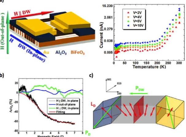
100]. Transport measurements as a function of temperature (4–300 K) along the 109° domain walls were conducted to reveal the conduction mechanism. As shown in Fig. 11, the transport results of 109° domain walls can be characterized by two distinct regimes. For the high-temperature regime (T > 200 K), the transport can be described through a thermally activated behavior, with an activation energy of ~0.25 eV, whereas the transport behavior is better de-scribed by a variable-range hopping (VRH) model [101] when it comes to the regime of temperatures below 200 K. In addition, the magnetotransport experiments revealed several intriguing phenomena. A remarkable negative magnetoresistance (MR) was observed when both mag-netic field and transport were parallel to the homointer-faces, as shown by the black curve of Fig. 11b. Negative MR values as high as ~60% were observed under a mag-netic field up to 7 T. It is more striking that very little MR is measured when the magnetic field was applied perpen-dicular to the transport direction (green curve of Fig. 11b). To explain the microscopic origins of the MR behavior, a general theme is the magnetic-field dependence of the core spin orientation and the influence on electron trans-port. To simplify the explanation of the complex behavior, Fig. 11c illustrates the 2 domains on either side of the 109° domain wall. Previous studies have shown that the spin
spiral in the bulk of BFO is broken when prepared in thin-film form. The energy degeneracy of the easy plane of magnetization ((111) plane in the bulk) is broken due to the imposed epitaxial strain, resulting in the formation of an easy antiferromagnetic axis of 112· Ò while the ferro-electric polarization is along the 〈111〉 axis [102]. The do-main-wall area is, therefore, those two antiferromagnetic easy axes rotate to merge, exhibiting a combination of Neel and Bloch types of domain wall. The antiferromag-netic easy axis in the domain wall, 0 12 ,· Ò can be deter-mined at the angle bisector of these two axes, which is in the domain-wall plane and mainly pointing out of plane of the sample surface, (001). Moreover, the rotation of ferro-electric polarization results in a net polarization perpen-dicular to the wall plane, which makes the domain-wall plane an easy plane for the spins to cant with the ap-plied external magnetic field [103]. As a result, we can ex-pect an anisotropy of magnetoresistance, which shows the largest value with the applied magnetic field along the do-main-wall direction. A detailed transport model has been proposed and discussed in Ref. [100]. The striking elec-tronic structures together with the fact that the nanoscopic feature of the domain wall, in which ~2 nm width of do-main wall, were experimentally revealed by Chiu et al. [104] afterwards. The intriguing magnetoelectric behavior,
Figure 11 Magnetotransport of 109° domain walls in BiFeO3 thin films. (a) Measurement device configuration (left) and temperature-dependent current–voltage curves (right). (b) Magnetoresistance as a function of magnetic fields and (c) a schematic of the evolution of antiferromagnetic easy axis as well asferroelectric polarizations within onesingle domain wall [100].
nanosized feature and switchable domain walls have made such homointerfaces a potential candidate for the next gen-eration of nanoelectronics.
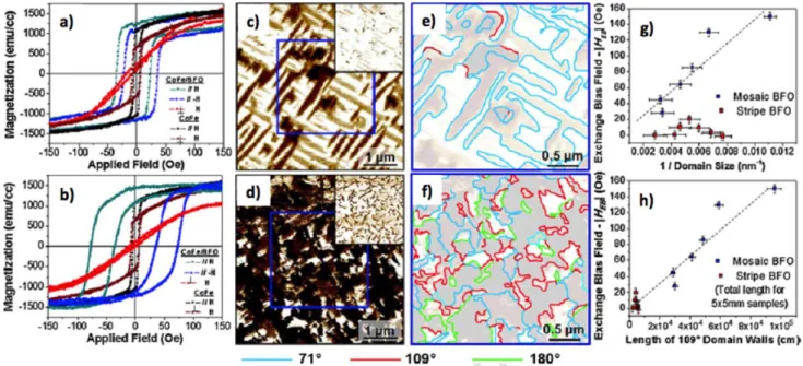
It is the tangled ferroic order parameters that enrich the fascinating properties and promising couplings. With the well-developed domain-engineering approaches, the one-dimensional periodic 71° and 109° domain patterns have served as the simplified and model platforms for us to gain further insights into the homointerfaces. A recent study found that a correlation exists not only to the density of domain walls, but also the density of certain types of do-main walls that determine the magnetic coupling with other ferromagnetic materials [63]. As shown in Fig. 12, two distinctly different types of magnetic properties were observed in CoFe/BFO heterointerfaces. Further experi-mental work has confirmed the role of the domain-wall types in determining the exchange bias interaction, which takes place between pinned, uncompensated spins occur-ring at domain walls in BFO and spins in the CoFe layer. The interaction gives rise to the shifts of the magnetic hys-teresis loop of the ferromagnetic layer. It has been revealed that the 109° domain walls exhibit significantly enhanced exchange bias, furthermore, an exchange enhancement in-teraction has arisen from an inin-teraction of the spins in the ferromagnet and the fully compensated (001) surface of the BFO 109° domain walls, which results in an enhancement of the coercive field of the ferromagnetic layer.
3.3 Future perspective of functional homo-interfaces The intriguing properties and rich phenomena
of domain walls form a growing and exciting field of
inter-est. The modulation of the adjacent domains gives rise to the entirely different functionalities at the walls. Therefore, in addition to discovering new phenomena within the ho-mointerfaces, how to locally trigger or control the func-tionalities will always be the focal key toward real applica-tions. The aforementioned SPM-based studies have opened up a way towards modulations of the domain-wall proper-ties [64, 72, 97]. Several applications have been proposed to make use of the homointerfaces in ferroic systems based on their conjugation and effects on existing devices [65]. Other combinations include optical applications, piezoelec-tric actuators, surface acoustic wave devices and nonvola-tile memories. A general question to ask is whether the as-sumptions made based on discontinuity of heterointerfaces are valid within the homogenous materials. Despite the fact that both experimental discoveries and theoretical investi-gations have prospered in recent years, further examination remains to be explored. Challenges remain to determine whether such fascinating functionalities can be controlled at sufficiently high speeds and densities to enable new logic device on the nanoscale. The factors such as switch-ing speed, domain switchswitch-ing, motion dynamics and corre-sponding size effects need to be carefully studied to verify if the functional walls could be developed as a fundamental block for high-density storage, communication processing systems or other advanced applications. Still another im-portant aspect of multiferroic domain walls also concerns the advanced functionalities, such as to introduce super-conductivity and metal–insulator transitions among the homointerfaces. More efforts are being made and will trig-ger more studies in the future. In summary of the homo-
Figure 12 Exchange bias study on various domain structures: Room-temperature magnetic properties for CoFe/BiFeO3 heterointer-face exhibiting exchange enhancement (a) and exchange bias (b) properties. (c), (d) Out-of-plane (inset) and in-plane PFM contrasts of BFO films that exhibit exchange enhancement and exchange bias, respectively. Detailed domain-wall distribution for (e) stripe-like and (f) mosaic-like BFO thin films. (g) CoFe/BiFeO3 exchange bias as a function of domain size and (h) exchange bias field as a func-tion of the total length of 109° domain walls/sample surface area in the same sample [63].
interface section, owing to the interplays of the electronic and magnetic orders at the domain walls, the nanoscale homointerfaces in complex oxide have spawned exciting and growing interests for functional materials and potential nanoelectronics. The dramatic progress in thin-film growth and domain engineering has served as focal keys to speed up these discoveries. We hope this chapter has captured some of the exciting studies in developing the homointer-faces, which also shed light on the promising applications.
4 Tubular interfaces
4.1 Evolution of tubular interfaces (TI) In this last
section, we will discuss the third kind of functional inter-faces, tubular interinter-faces, which are usually seen in vertical heteroepitaxial self-assembled systems (Fig. 1c). Vertical heteroepitaxial nanocomposites are composed of two dif-ferent materials possessing desirable characteristics. Nu-merous studies showed that the intriguing properties of self-assembled nanocomposites can be enhanced or created through an interface-mediated coupling [105] or local con-finement mechanisms [106]. These self-assembled systems have resulted in strengthened magnetoelectric coupling in ferroelectric BaTiO3-ferrimagnetic CoFe2O4 [107],
enhanced ferroelectricity in BaTiO3–Sm2O3 [108],
photo-magnetic coupling in photostrictive SRO-magnetostrictive CFO [109] and colossal magnetoresistance driven at low magnetic field in (La0.7Sr0.3)MnO3–ZnO2 [106]. For
creat-ing or enhanccreat-ing functional properties via couplcreat-ing
be-tween different (use “ordered” or “other”) parameters [106, 109–111], workers have tried to gain further understanding of fundamental mechanisms via both experimental and theoretical methods. As theoretical pioneers, Newnham and Trolier-McKinstry have summarized the structure connectivity between two materials in composites as well as how the properties will be modified or enhanced [112]. In addition, Hill concluded that a driving force is necessary for magnetism and electricity to coexist in multiferroic magnetoelectric materials by conducting density functional theory calculations [113]. Among various self-assembled systems, vertical heteroepitaxial nanocomposites have of-fered promising capabilities to create intriguing functional-ities through the interplays between different degrees of freedom and external stimuli of the selected materials [8, 15, 106]. It is the tubular interfaces between different spe-cies of the vertical nanocomposites that enable us to create interesting phenomena and to trigger new possibilities.
4.2 BFO/CFO tubular interfaces The fascinating
features of heterointerfaces and homointerfaces mentioned in the foregoing paragraphs have been established. In addi-tion to the two kinds of oxide interfaces, which have been explored widely, tubular interfaces have emerged as one of the focal points in developing new functional interfaces. Those tubular interfaces are usually found in the self-assembled nanostructure systems [7, 107, 110], and serve as a main role to mediate the local disorders and the emerg-
Figure 13 (a) Typical morphology of a BFO–CFO nanostructure; (b) the image of one CFO nanostructure; (c) high-resolution image of interface between BFO and CFO, corresponding to the yellow frame in (b); (d) schematic image of the interface between BFO and CFO; (e) cross-sectional TEM image of one CFO nanostructure; (f) plane-view image of BFO–CFO by SEM; (g) and (h) schematics of CFO facet configuration [114].
ing phenomena. The first central feature of the tubular in-terface was recognized by Hsieh et al. in 2013, in which a tunable conducting interface was found in self-assembled perovskite BFO-spinel CoFe2O4 (CFO) nanostructure [7].
To identify and explore the structural and emerging phe-nomena, high-resolution transmission electron microscopy is used to reveal the structural correlation of tubular oxide interfaces in detail, while scanning probe microscopy and scanning tunneling microscopy are optimal techniques for discovering the local properties on the nanoscale.
Within the scope of the BFO–CFO nanostructure sys-tem, the structural nature and evolution can be character-ized by transmission electron microscope (TEM) [114], as shown in Fig. 13. CFO nanopillars are embedded in the BFO matrix with a distinguishable contrast from the TEM image in Fig. 13a. The image of cross-sectional TEM showed that due to the difference of surface energy be-tween BFO and CFO [115]. BFO and CFO were spontane-ously separated during the heteroepitaxial growth process, forming BFO matrix and CFO nanopillars on an STO(001) substrate, respectively. Zheng et al. have analyzed the structural relationship of the BFO–CFO system and shown that the interfaces between BFO and CFO grown on STO(001) substrate are {110} planes [114]. Further
ex-periment conducted by Zhan et al. have pointed out the most stable configuration of the interface between perovskite and spinel is a semicoherent interface
con-structed by [BiFeO]4+ of BFO and [(Ni, Fe)O
2]1.5– of
NiFe2O4 [116]. Hence, a thorough configuration at the
BFO/CFO interface could be constructed.
Regarding the nanoscale feature of the tubular oxide interfaces, the scanning probe microscopy is the optimal option and has been used to characterize local electronic properties [64, 90, 97]. Conducting behaviors at the tubular oxide interfaces were observed by C-AFM [7], by which a nonvolatile switching modulation was achieved. Figure 14 shows the examination of the conducting current distribu-tion on the BFO–CFO sample on the nanoscale. During the measurement of CAFM, the images of topography and cur-rent distribution can be recorded simultaneously. The topography, which is consistent with previous TEM results, illustrated a BFO matrix and CFO nanopillars and the im-age of current distribution also clearly shows that the sig-nal of current can be detected with a small sample bias and the enhanced conduction was observed at the tubular oxide interface region between the CFO nanopillar and the BFO matrix. Comparing the profile of the CFO nanopillar with current signals at different sample bias shows that the cur-
Figure 14 Probing the local conduction at tubular oxide interfaces: (a) Topography and (b) conductive-AFM images taken at the same area with a sample bias of 0.05 V applied to the sample surface; (c) comparison between topography and current profiles in the same cross section; (d) I–V curves measured near and off the interface. The symbol dots in the inset AFM image indicate the positions to measure corresponding I–V curves plotted by the same symbol [7].
![Figure 8 Schematic of (a) 109°, (b) 71° and (c) 180° domain walls in BiFeO3 with respect to predicted stacks [90]](https://thumb-ap.123doks.com/thumbv2/9libinfo/7532333.119928/11.892.180.692.147.322/figure-schematic-domain-walls-bifeo-respect-predicted-stacks.webp)
![Figure 10 Boundary conditions for domain-wall engineering in BiFeO 3 . (a) The electrostatic boundary condition provided by the SrRuO 3 bottom electrode and the elastic boundary condition provided by the anisotropic strain of DyScO 3 substrate [99]](https://thumb-ap.123doks.com/thumbv2/9libinfo/7532333.119928/13.892.139.749.651.1050/boundary-conditions-engineering-electrostatic-condition-condition-anisotropic-substrate.webp)