Amorphous-Layer Regrowth and Activation of P and
As Implanted Si by Low-Temperature
Microwave Annealing
Fu-Kuo Hsueh, Yao-Jen Lee, Kun-Lin Lin, Michael I. Current, Ching-Yi Wu, and Tien-Sheng Chao
Abstract—Microwave annealing of dopants in Si has been re-ported to produce highly activated junctions at temperatures far below those needed for comparable results using conventional thermal processes. However, the details of the kinetics and mech-anisms for microwave annealing are far from well understood. In this paper, 20-keV arsenic (As) and 15-keV phosphorus (P) implants, in a dose range from 1 to 5× 10¹⁵ ion/cm2, were annealed by microwave methods at temperatures below 500◦C. These junctions were characterized by profile studies with sec-ondary ion mass spectrometry and spreading resistance profiling, sheet resistance with four-point probe, and extensive use of cross-sectional transmission electron microscopy to follow the regrowth of the as-implanted amorphous layers created by the implantation. The amorphous-layer regrowth was observed to be uneven in time, with relatively little amorphous/crystalline interface motion for less than 50 s, followed by rapid regrowth for longer times. Sheet resistance values continued to drop for anneal times after the regrowth process was complete, with some evidence of dopant deactivation for anneal times of 600 s.
Index Terms—Low temperature, microwave annealing, solid-phase epitaxily growth (SPEG).
I. INTRODUCTION
I
N SCALING down the physical gate length of metal–oxide– semiconductor field-effect transistors to 17 nm by 2015 to meet the International Technology Roadmap for Semi-conductors 2009 (ITRS 2009) [1], several challenges must be overcome. One of the main challenges in fabricating a front-end process for high-performance devices is accurate control of the placement of the active doping regions, with junctionManuscript received January 26, 2011; revised March 13, 2011; accepted March 15, 2011. Date of publication April 7, 2011; date of current version June 22, 2011. This work was supported in part by the National Science Council, Taiwan, under Contract NSC-99-2221-E-491-031-MY2 and Contract NSC-98-2221-E-212-033-MY3. The review of this paper was arranged by Editor H. Shang.
F.-K. Hsueh is with the National Nano Device Laboratories, Hsinchu 30078, Taiwan, and also with the Department of Electrophysics, National Chiao Tung University, Hsinchu 30050, Taiwan.
Y.-J. Lee is with the National Nano Device Laboratories, Hsinchu 30078, Taiwan, and also with the Department of Physics, National Chung Hsing University, Taichung 402, Taiwan (e-mail: [email protected]).
K.-L. Lin is with the National Nano Device Laboratories, Hsinchu 30078, Taiwan.
M. I. Current is with Current Scientific, San Jose, CA 95124 USA. C.-Y. Wu is with Bayzu Precision Co., Tainan 74144, Taiwan.
T.-S. Chao is with the Department of Electrophysics, National Chiao Tung University, Hsinchu 30050, Taiwan.
Color versions of one or more of the figures in this paper are available online at http://ieeexplore.ieee.org.
Digital Object Identifier 10.1109/TED.2011.2132801
depths targeted for less than 7.3 nm for the reduction of short-channel effects. However, shallow junction depths would increase higher junction resistance, resulting in increased power dissipation and lower circuits drive currents and speeds [2]. To keep the junction and contact resistances low, high-temperature anneals have been extensively studied to electrically activate implanted dopants and repair lattice damage created during ion implantation to reduce junction leakage currents. These high-temperature anneals include msec flash and laser pulses above 1200◦C [3], “spike” anneals for about 1 s at 1050◦C [4], solid-phase epitaxy anneals at about 700 ◦C, and combinations of spike + msec annealing or msec + spike anneal [5]. Although all of these methods have demonstrated some successful appli-cation to the source/drain anneal, they all entail a number of problems that make processing more complicated. This is be-cause the source/drain extension in the devices simultaneously requires shrinking junction depths and improved abruptness to increase device performance with a high transistor drive current and a short delay time [6]. In addition, msec annealing methods can create uneven heating of circuit elements due to emissivity differences in near-surface device materials and limited phonon diffusion distances for msec and shorter anneals [7].
Microwave heating of silicon allows for more even volumet-ric heating of the wafer due to the greater penetration depth as-sociated with microwave processing [8]. In addition, microwave annealing presents an appealing potential solution, because it takes place at a low temperature that restrains diffusion yet still results in good dopant activation. Arsenic and boron activation in a Si substrate by low-temperature microwave heating from 450◦C to 650◦C has been demonstrated, with dopant diffusion effectively suppressed [9]. In addition, a strained 3-nm Ge epilayer on a boron-implanted Si substrate was also preserved using low-temperature microwave anneal [10].
However, the details of the kinetics and mechanisms for microwave annealing are far from well understood. In this paper, characteristics of activation and de-activation of P and As implants through solid-phase epitaxily growth (SPEG) by a low-temperature (< 500 ◦C) microwave annealing process was studied. Cross-sectional transmission electron microscopy (TEM) pictures were performed to evaluate the rates of SPEG during the microwave annealing process on highly damaged layers of P and As ion-implanted silicon samples. Rs of P and As junctions formed with different ion doses and annealed for different microwave annealing times were also measured and compared. Secondary ion mass spectrometry
range from 1× 10 to 5× 10 ion/cm . To minimize ion channeling effects, all wafers were oriented during implantation with their surface normal at 7◦from the incident beam and with a 22◦in plane twist.
Microwave annealing process at temperatures below 500◦C was used. Wafer temperatures during the microwave anneal were monitored by a pyrometer with a direct line of sight to the lower surface of a three-wafer stack in the chamber [11]. Before the microwave annealing process, a 10-min nitrogen purge was performed and maintained until the process was completed. The frequency of the microwave was 5.8 GHz. The microwave annealing process time was defined as the duration for which the microwave magnetron was turned on. Microwave magnetron power was about 2100 W, using an AXOM-300, which is a highly multimoded chamber manufactured by DSG Technologies.
To investigate the characteristics of dopant activation or de-activation and to evaluate the rates of SPEG during the microwave annealing process, different microwave annealing dwell times (50, 75, 100, 300, and 600 s) were performed. In addition, to keep the process temperature under 430◦C for a longer dwell time, six microwave annealing cycles of 100 s each, totaling to 600 s, were also carried out, where the mi-crowave power was kept constant during the anneal process cycle, with 30-min pauses between each cycle. After the mi-crowave annealing process, Rs with four-point probe, SIMS profile, SRP, and cross-sectional TEM images, were measured and compared.
III. RESULTS ANDDISCUSSIONS
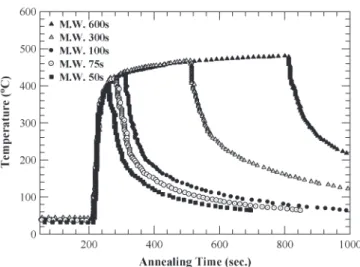
Fig. 1 depicts the microwave annealing temperature profiles versus annealing time. The peak anneal temperatures on the wafer were 430◦C, 465◦C, and 480◦C if the microwave mag-netrons were turned on for 100, 300, and 600 s, respectively. Although SiC microwave susceptors could be used to allow obtaining higher surface temperature ranging from 500 ◦C to 650◦C [9], they were not used in this paper.
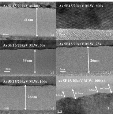
In order to evaluate the rate of SPEG in ion-implanted silicon samples by low-temperature microwave annealing, cross-sectional TEM images were performed on P-implanted (15 keV and 1–5× 10¹⁵ ion/cm2) and As-implanted (20 keV and 1–5× 15 ion/cm2) samples. Figs. 2 and 3 show cross-sectional TEM images of the P- and As-implanted samples at a dose of 5× 10¹⁵ ion/cm2. In Figs. 2(a) and 3(a), the
Fig. 1. Comparison of temperature profiles versus annealing time. The mi-crowave annealing time was defined as the period when the mimi-crowave power was turned on. The maximum temperatures were 430◦C, 465◦C, and 480◦C as the microwave process times were 100, 300, and 600 s, respectively.
Fig. 2. Cross-sectional TEM pictures for P at 15 keV with 5× 10¹⁵ ion/cm−2of (a) as implanted, (b) 600 s, (c) 50 s, (d) 75 s, (e) 100 s,
and (f) 100 s× 6.
as-implanted samples contain amorphous layers with thick-nesses of 46 and 40 nm for the 15-keV P and 20-keV As, respectively. The amorphous region can be distinguished as the lightly shaded area in Figs. 2(a) and 3(a).
Fig. 2(b) contains the cross-sectional TEM image of the P-implanted sample after microwave annealing for 600 s, showing the excellent crystallinity of the regrown Si layer. The kinetics and mechanisms of the crystallinity regrowth during microwave annealing was SPEG, nucleating at the amorphous/crystalline (a/c) interface and proceeding toward the sample surface. In the cross-sectional TEM images of Fig. 2(c)–(e), there were still 41-, 21-, 13-nm-thick amorphous Si layers remaining after microwave annealing for 50, 75, and 100 s. The rates of SPEG of P-implanted samples, which were taken from the change in thicknesses of the amorphous Si layer
Fig. 3. Cross-sectional TEM pictures for As at 20 keV with 5× 10¹⁵ion/cm−2of (a) as implanted, (b) 600 s, (c) 50 s, (d) 75 s, (e) 100 s,
and (f) 100 s× 6.
of Fig. 2(c)–(e), were 0.1 nm/s < 50 s, 0.8 nm/s between 50 and 75 s, and 0.32 nm/s between 75 and 100 s, i.e., an average rate of 0.33 nm/s for the first 100 s. This is more than 102times faster than the regrowth for undoped Si(100) at 500◦C [12].
The a/c interface was still smooth for < 50-s microwave annealing process, which indicated that microwave annealing could nucleate and initialize SPEG at the a/c interface but with relatively little a/c interface motion, due to the lower wafer temperature during the early stages of the anneal process (see Fig. 1). Between 50 and 75 s, the SPEG rate increased from 0.1 to 0.8 nm/s, and Rs also improved from 650 to 160 Ω/sq. That is, most of the dopants could be activated during this period effectively.
Between 75 and 100 s, the rate of the SPEG of P-implanted samples was retarded and decreased from 0.8 to 0.32 nm/s. For longer annealing times, from 100 s to 300 or 600 s, the remaining amorphous Si layer could regain its crystallinity due to the longer dwell times and higher process temperature.
Next, to keep the process temperature under low (< 430◦C) temperature for a longer anneal time, six microwave annealing cycles of 100 s each, totaling to 600 s, were also carried out. Cross-sectional TEM images [see Fig. 2(f)] show excellent crystallinity. Therefore, from the results of Fig. 2, the crys-tallinity of the implanted Si layer depended on the microwave annealing time if one would like to limit the maximum temper-ature to below 430◦C.
Fig. 3(b) depicts the cross-sectional TEM images of the As-implanted samples (20 keV and 5× 10¹⁵ ion/cm2) after mi-crowave annealing for 600 s. The cross-sectional TEM picture also depicted excellent crystallinity of the annealed Si layer.
From the cross-sectional TEM images in Fig. 3(c)–(e), there were still 39-, 26-, and 26-nm-thick amorphous Si layers after the microwave annealing process for 50, 75, and 100 s,
respec-Fig. 4. Cross-sectional TEM pictures for P at 15 keV with 1× 10¹⁵ion/cm−2of (a) as implanted, (b) 50 s, (c) 75 s, and (d) 100 s.
tively. The rate of SPEG was 0.04 nm/s < 50 s and 0.52 nm/s between 50 and 75 s, with almost no SPEG between 75 and 100 s, i.e., an average rate of 0.15 nm/s for the first 100 s. In contrast to those of the P-implanted samples, the cross-sectional TEM images for the As-implanted samples [see Fig. 3(f)] showed that the amorphized Si layer was not fully recrystallized even by microwave annealing for 6× 100 s, although the 600-s anneal, with a higher peak temperature 480◦C, did recrystalize the As-implant damage layer [see Fig. 3(b)].
In addition, the roughness of the regrowing a/c interfaces increased markedly, to a max-min thickness range of 4 nm [Fig. 3(f)], as one increased the number of 100-s microwave annealing cycles, with a peak temperature 430◦C. This break-down of planar front regrowth behavior for longer anneal times at 430◦C is another indication that the regrowth kinetics for high-dose As annealing with microwaves is more difficult than lower doses and lighter ions, such as P.
Figs. 4 and 5 show the cross-sectional TEM images of P- and As-implanted samples at a dose of 1× 10¹⁵ ion/cm2. In Figs. 4(a) and 5(a), the thickness of the amorphous Si layers for As-implanted 15-keV P and 20-keV As was 35.9 and 34 nm, respectively. From the cross-sectional TEM image of Fig. 4(b), there was a residual 29.5-nm amorphous Si layer for the P-implanted samples after microwave annealing for 50 s, which was completely regrown for anneal times of 75 s. The rate of SPEG was 0.13 nm/s < 50 s and 1.18 nm/s between 50 and 75 s. From the cross-sectional TEM picture of Fig. 5(b) and (c), there were still 30- and 3.2-nm amorphous Si layers for the As-implanted samples after the microwave annealing process for 50 and 75 s. The rate of SPEG was 0.12 nm/s < 50 s and 1.12 nm/s between 50 and 75 s. After 100 s [Fig. 5(d)], the Si layer is completely recrystallized for these lower dose As implants.
Fig. 6 summarized the amorphous-layer thickness, which was measured by TEM, for As- and P-implanted layers for microwave annealing times of less than 100 s. The rates of SPEG in the first 50 s were slow due to the gradually rising temperature. However, the rates of SPEG increase drastically in the range of 50–75 s, as the anneal temperature stabilizes at about 420 ◦C. The observed slowing of the regrowth rates for anneal times longer than 75 s for the higher dose implants
Fig. 5. Cross-sectional TEM pictures for As at 20 keV with 1× 10¹⁵ion/cm−2of (a) as implanted, (b) 50 s, (c) 75 s, and (d) 100 s.
Fig. 6. Amorphous-layer thickness, as measured by TEM, for As- and P-implanted layers for microwave anneal times of less than 100 s.
may be related to an increase in the reflection of the microwave power by the doped surface layer as the surface conductivity is increased by the anneal process.
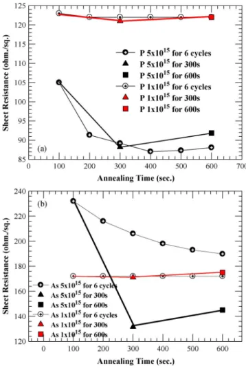
The average magnitudes of Rs for all the splits after the microwave annealing process were summarized in Fig. 7(a) and Fig. 7(b) for P- and As-implanted samples, respectively. For the P implants, Fig. 7(a), with a dose of 5× 10¹⁵ion/cm2, the Rs could be reduced from 105 to 88.2 Ω/sq as the microwave annealing time was increased from 100 to 300 s, well after the SPER process is complete. However, for longer annealing times, from 300 to 600 s, Rs was increased from 88.2 to 91.2 Ω/sq, with 4% dopant deactivation occurred. The 6× 100 s anneals (with a peak temperature of 430◦C) and the higher dose P implants resulted in similar Rs values at 100 and 300 s and less dopant deactivation at 600-s total time than the “single-shot” (and higher peak temperature) 600-s anneal. The higher dose As implants resulted in more complex Rs trends, with lower Rs values for the “single-shot” 300- and 600-s anneals than the 6× 100-s cycles, which continued to decrease out to the sixth cycle. The 600-s anneal case for the high-dose As re-sulted in a 7.7% higher Rs than the 300-s anneal, again indicat-ing some degree of dopant deactivation for longer anneal times. For both P and As implants at lower (1× 10¹⁵ ion/cm2) doses, the Rs values did not show any strong variations for
Fig. 7. Sheet resistance (Rs) of all splits for (a) P and (b) As by low-temperature microwave annealing process.
anneal times between 100 and 600 s. For the As case, the lower dose Rs value was higher (≈172 Ω/sq) than the higher dose values for the single-shot 300- and 600-s anneal but lower than the trend for the higher dose 6× 100-s cycles.
The definition of Rs is given as follows [13]:
Rs= 1/[uave∗ N ∗ q] where
uave average carrier mobility (in square centimeters per volt-second);
N active carrier dose (in carriers per square centimeters);
E electron charge.
The average mobility uavedepends on the carrier and scatter defect concentrations in the junction. Therefore, Rs magnitude after low-temperature microwave annealing process was deter-mined by the implant dose and SPEG process.
In Fig. 7(b), the Rs of As-implanted samples with a dose of 5× 10¹⁵ ion/cm2 could be reduced from 236.2 to 131.8 Ω/sq as the microwave annealing time was carried out from 100 to 300 s. However, as the microwave annealing time was increased from 300 to 600 s, the Rs increased from 131.8 to 145 Ω/sq, implying that a 10% dopant deactivation occurred.
In contrast to the results of P-implanted samples, the Rs of As-implanted samples with a dose of 5× 10¹⁵ ion/cm2 was
Fig. 8. SIMS profiles of (a) P and (b) As concentration at a dose of 5× 10¹⁵ion/cm2. The P distribution after the spike annealing showed a deeper
dopant diffusion, whereas the As distribution was only slightly deeper for the spike anneal. The microwave anneal process resulted in no significantly dopant diffusion in either case.
reduced only slightly, from 236.2 to 188 Ω/sq, during the six repeated cycles of 100-s anneal times.
For lower implant doses, 1× 10¹⁵ ion/cm2, the Rs values for both As- and P-implanted samples were saturated at fixed values after 100-s annealing and did not change as the anneal exposure was increased to 600 s (see Fig. 7). This implies that the dopant activation was nearly complete for these doses after the 100-s microwave anneal at a peak temperature of 430◦C. In addition, at this lower dose, the regrowth of the amorphous layers created by the As and P implants was complete after 100 s [Figs. 4(d) and 5(d)]. The apparent increase in the amorphous-layer regrowth rates for the lower dose implants, which was especially clear for the As cases (see Fig. 6), is opposite to the trends observed for conventional thermal anneals of As and P at similar temperatures monitored by optical reflectance and RBS [12].
Fig. 8 shows the SIMS profiles of the 15-keV P [Fig. 8(a)] and 20-keV As [Fig. 8(b)] concentrations. After 1000◦C spike anneals, the P profile showed substantial diffusion in the peak and tail regions, whereas the As profile showed only a modest broadening of the mid-range profile. All of the dopant profiles after the low-temperature microwave anneals were
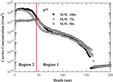
indistin-Fig. 9. SRP profiles of P implants, at a dose of 5× 10¹⁵ ion/cm2, after
the 100-, 75-, and 50-s microwave annealing process, which indicates the profiles of the active dopant concentration. The vertical red line at 45 nm is the approximate location of the a/c interface after 50-s microwave anneal.
guishable from the as-implanted profiles, indicating no dopant diffusion motion for these < 500◦C anneals.
The SRP profiles (Fig. 9) of the 15-keV P implants with a dose of 5× 10¹⁵ ion/cm2 after 50, 75, and 100 s showed peak active dopant concentrations of 3× 10²⁰carrier/cm3after 75- and 100-s anneals. The active carried concentration at the partially regrown amorphous-crystalline interface for the 50-s anneal was 2× 10¹⁹carrier/cm3, which aligned well with the profiles at a depth of 45 nm for the fully regrown cases for the longer anneals. The relatively high levels of active carriers, i.e., ≈1 × 10¹⁹ carrier/cm3, seen by the SRP analysis in the remaining amorphous layer after the 50-s anneal (Region 2 in Fig. 9) indicated that significant dopant annealing occurs in the amorphous region prior to the arrival of the crystalline growth front for the microwave annealing process.
The SPR analysis of carrier concentrations assumes a carrier mobility taken from analysis of crystalline material. Further detailed measurements by Hall methods of the carrier concen-trations and mobilities in the residual amorphous Si regions after microwave anneals would be most instructive.
IV. CONCLUSION
In this paper, activation and deactivation of P and As im-plants by a low-temperature (< 500◦C) microwave annealing on implanted Si samples without SiC susceptors have been demonstrated and compared. The rates of SPEG of P- and As-implanted samples have been both evaluated, and they have depicted low–high–low rates of SPEG during the microwave annealing process. The rates of SPEG have been faster for the implanted samples in a lighter dose (1× 10¹⁵ ion/cm2) than these in a heavier dose (1× 10¹⁵ion/cm2). The Rs magnitudes of P and As at a dose of 5× 10¹⁵ion/cm2could be suppressed to 88.2 and 131 Ω/sq, respectively, as the annealing time was extended to 300 s, after the SPEG process was completed. As one increases the anneal time from 300 to 600 s, a small but measureable level of dopant deactivation occurred. Finally, from the comparisons between cross-sectional TEM pictures and SRP profiles, there were two mechanisms of dopant
Available: http://www.itrs.net/
[2] D. K. Schroder, Semiconductor Material and Device Characterization. Hoboken, NJ: Wiley, 2006.
[3] Q. Zhang, J. Huang, N. Wu, G. Chen, M. Hong, L. K. Bera, and C. Zhu, “Drive-current enhancement in Ge n-channel MOSFET using laser an-nealing for source/drain activation,” IEEE Electron Device Lett., vol. 27, no. 9, pp. 728–730, Sep. 2006.
[4] A. T. Fiory, H.-J. Gossmann, C. Rafferty, P. Frisella, J. Hebb, and J. Jackson, “Ultra-shallow junctions and the effect of ramp-up rate dur-ing spike anneals in lamp-based and hot-walled RTP systems,” in Proc.
Int. Conf. Ion Implantation Technol., Kyoto, Japan, Jun. 22–26, 1998,
pp. 22–25.
[5] C. F. Nieh, K. C. Ku, C. H. Chen, H. Chang, L. T. Wang, L. P. Huang, Y. M. Sheu, C. C. Wang, T. L. Lee, S. C. Chen, M. S. Liang, and J. Gong, “Millisecond anneal and short-channel effect control in Si CMOS transistor performance,” IEEE Electron Device Lett., vol. 27, no. 12, pp. 969–971, Dec. 2006.
[6] W. Aderhold, I. Iliopoulos, and A. Hunter, “Virtual metrology in RTP with WISR,” in Proc. 15th IEEE Int. Conf. Adv. Therm. Process.
Semicond.—RTP, 2007, pp. 101–104.
[7] J. D. Plummer, M. D. Deal, and P. B. Griffin, Silicon VLSI
Technol-ogy: Fundamentals, Practice and Modeling. Upper Saddle River, NJ:
Prentice-Hall, 2000.
[8] E. L. Pankratov, “Redistribution of dopant during microwave annealing of a multilayer structure for production p–n junction,” J. Appl. Phys., vol. 103, no. 6, p. 064 320, Mar. 2008.
[9] T. L. Alford, D. C. Thompson, J. W. Mayer, and N. D. Theodore, “Dopant activation in ion implanted silicon by microwave annealing,” J. Appl.
Phys., vol. 106, no. 11, p. 114 902, Dec. 2009.
[10] Y.-J. Lee, F.-K. Hsueh, S.-C. Huang, J. M. Kowalski, J. E. Kowalski, A. T. Y. Cheng, A. Koo, G.-L. Luo, and C.-Y. Wu, “A low-temperature microwave annealing process for boron-doped ultrathin Ge epilayer on Si substrate,” IEEE Electron Device Lett., vol. 30, no. 2, pp. 123–125, Feb. 2009.
[11] Y.-J. Lee, S.-S. Chuang, F.-K. Hsueh, H.-M. Lin, S.-C. Wu, C.-Y. Wu, and T.-Y. Tseng, “Dopant activation in single crystalline germanium by low temperature microwave annealing,” IEEE Electron Device Lett., vol. 32, no. 2, pp. 194–196, Feb. 2011.
[12] G. L. Olsen and J. A. Roth, “Kinetics of solid phase crystallization in amorphous silicon,” Mater. Sci. Rep., vol. 3, no. 1, pp. 1–77, 1988. [13] S. Prussin, J. Reyes, H. Onoda, N. Hamamoto, M. Tanjyo, S. Umisedo,
Y. Kawamura, M. Hashimoto, Y. Koga, N. Maehara, Y. Nakashima, H. Yoshimi, S. Sezaki, and M. Current, “Optimization of implant and anneal processes,” in Proc. 18th IEEE Int. Conf. Adv. Therm. Process.
Semicond.—RTP, 2010, pp. 86–89.
Fu-Kuo Hsueh was born in Taipei, Taiwan, in 1980.
He received the M.S. degree in semicondutor mate-rials and process equipment, in 2010, from National Chiao-Tung University, Hsinchu, Taiwan, where he is currently working toward the Ph.D. degree in the Department of Electrophysics, where he has worked on CMOS devices fabrication and semiconductors for thin-film electronic devices.
He joined the National Nano Device Laboratories, Hsinchu, as an Engineer, in July 2006. More recently, he began work in microwave annealing of ion implantation.
From 2006 to 2008, he was a Postdoctoral Researcher with National Chiao-Tung University and National Taiwan University of Science and Technology, Taipei, Taiwan. Among these, he con-ducted the microstructural characterization on metal/ ceramic interface by transmission electron mi-croscopy (TEM). From 2008 to 2010, he was with the Physical Failure Analysis Department, Inotera Memories Inc., Taoyuan, Taiwan, and worked on TEM analysis on dynamic random-access memory. Since May 2010, he has been an Associate Researcher with the National Nano Device Laboratories, Hsinchu. His research interests are TEM analysis on materials characterization.
Michael I. Current received the Ph.D. degree in
phy-sics from Rensselaer Polytechnic Institute, Troy, NY. He has worked for more than three decades on ion-beam processing and analysis of materials and devices for integrated-circuit and photonic appli-cations. He has held research and technical man-agement positions at Applied Materials, Signetics/ Philips; Xerox Palo Alto Research Center, Palo Alto, CA; Frontier Semiconductor, San Jose, CA; Cornell University, Ithaca, NY; and Kyoto University, Kyoto, Japan, as well as startups, Trilogy Systems, and Silicon Genesis. He is currently with Current Scientific, San Jose, CA.
Ching-Yi Wu was born in Chia-Yi, Taiwan, in 1957.
He received the Ph.D. degree in electronics engineer-ing from National Tsengineer-ing-Hwa University, Hsinchu, Taiwan, in 1987.
Since 1987, he has been with the Industrial Technology Research Institute (ITRI), Hsinchu, working for 17 years. He was the Director General of Micro Systems Laboratories and the Deputy Director General of the Electronics Research and Service Organization, ITRI. His professional fields are semiconductor, optoelectronics, and micro-electromechanical systems. Since 1990, he has been a Part-Time Professor with National Taiwan University, Taipei, Taiwan, and National Tsing-Hwa University, Hsinchu, working for 20 years. Since 2004, he has been with stock-sharing private companies, as General Manager and Board of Director, in the areas of micropackage, flexible package, and thin-film processing. He is currently with Bayzu Precision Co., Tainan, Taiwan.
Tien-Sheng Chao was born in Penghu, Taiwan, in
1963. He received the Ph.D. degrees in electronics engineering from National Chiao Tung University, Hsinchu, Taiwan, in 1992.
He joined the National Nano Device Laborato-ries (NDL), Hsinchu, as an Associate Researcher, in July 1992 and became a Researcher in 1996. He was engaged in developing the thin dielectrics preparations, cleaning processes, and complemen-tary metal–oxide–semiconductor device fabrication. Then, he joined the Department of Electrophysics, National Chiao Tung University, in 2001 and became as a Professor in 2002.